kevan thompson - simon fraser universitywhitmore/courses/ensc305/projects/2010/12desi.pdf ·...
TRANSCRIPT

March 08, 2010
Dr. Andrew Rawicz School of Engineering Science Simon Fraser University Burnaby, British Columbia V5A 1S6 Re: ENSC 440 Design Specification for an Implementation of a Smart House using Power Line Communication Dear Dr. Rawicz: The attached document, Design Specification for an Implementation of a Smart House using Power Line Communication, outlines the high level design requirements of our project for ENSC 440 (Capstone Engineering Science Project). We intend to research and implement a programmable power line modulation system, called Prometheus, which enables users to remotely check and control the status of the lights inside their buildings, through the structures existing power grid. The purpose of this design specification report is to describe the high level design requirements for both the proof-of-concept and final product. This document will be used by all members of the Nexus Technologies as a guideline for design, development, and testing of the Prometheus system. The Nexus team consists of five intellectual, highly motivated, and talented fourth-year engineering students: Kia Filsoof, Pranil Reddy, Yalda Hakki, Mike Kubanski, and Kevan Thompson. If you have any questions or concerns about our design specification report, please feel free to contact me by phone at (604)910-5747 or by e-mail at [email protected] Sincerely,
Kevan Thompson Kevan Thompson Chief Executive Officer Nexus Technologies
Enclosure: Design Specification for a Smart House using Power Line Communication System
Design Specification for Smart House with Power Line Communication Network
Project Team: Pranil Reddy Kia Filsoof Yalda Hakki Kevan Thompson Michael Kubanski
Contact Person: Kevan Thompson [email protected]
Submitted to: Dr. Andrew Rawicz – ENSC 440 Mr. Steve Whitmore – ENSC 305 School of Engineering Science Simon Fraser University
Issued date: March 8, 2010 Revision: 0.1

iii
Executive Summary The design specification for the Prometheus Home Automation System provides a detailed description of the design and development of our proof-of-concept and final product. Therefore, we will discuss design considerations pertaining to the functional requirements marked I, II, or III as specified in the document Functional Specification for Smart House with Power Line Communication Network [1]. This document outlines the design of the Prometheus system and provides justification for our design choices. The Master Controller will consist of a TS-7200 Single Board Computer which will provide a web interface to users, and will communicate data to the Device Controllers. The Device Controllers will consist of PIC 16F877A microcontrollers, as well as power MOSFETs and relays to control the devices. The Master Controller and Device Controllers will communicate over the power lines. Data will be modulated on the power lines using a Frequency Shift Keying modulation scheme and coupling transformers. The modulation is accomplished using a Voltage Controlled Oscillator, and the demodulation is accomplished using a Phase Locked Loop. This report will include a detailed description of the resources required to complete the project, as well as circuit schematics, software flow charts, and network control protocols.

iv
Contents
Executive Summary ...................................................................................................................................... iii
List of Figures ............................................................................................................................................... vi
List of Tables ................................................................................................................................................ vi
Glossary ....................................................................................................................................................... vii
1. Introduction .......................................................................................................................................... 9
1.1 Scope ............................................................................................................................................. 9
1.2 Intended Audience ........................................................................................................................ 9
2. System Specification ........................................................................................................................... 10
3. Overall System Design ......................................................................................................................... 10
3.1 High Level System Design ........................................................................................................... 10
3.2 Electrical Design .......................................................................................................................... 11
3.2.1 Power Supply Requirements ............................................................................................... 11
3.3 Mechanical Design ...................................................................................................................... 12
3.3.1 Master Controller Enclosure ................................................................................................... 12
3.3.2 Device Controller Enclosure .................................................................................................... 13
4. Master Controller Design .................................................................................................................... 14
4.1 Purpose ....................................................................................................................................... 14
4.2 RS232 Module Design ................................................................................................................. 15
4.3 Internet Webpage/User Interface Design ................................................................................... 15
4.4 Network Module Design ............................................................................................................. 16
5. PLCM Design ....................................................................................................................................... 17
5.1 Purpose ....................................................................................................................................... 17
5.2 Modulator Circuit Design ............................................................................................................ 18
5.3 Coupling Circuit Design ............................................................................................................... 21
5.4 Decoupling/Signal Conditioning Circuit Design .......................................................................... 22
5.5 Demodulator Circuit Design ........................................................................................................ 23
5.6 Safety Issues ................................................................................................................................ 25
6. Device Controller Design ..................................................................................................................... 26
6.1 Purpose ....................................................................................................................................... 26
6.2 PIC Design.................................................................................................................................... 26
6.2.1 RS232 Module ..................................................................................................................... 27
6.2.2 Signal Handling .................................................................................................................... 28

v
6.3 Hardware Design ......................................................................................................................... 28
7. System Test Plan ................................................................................................................................. 30
7.1 Master Controller Unit Tests ....................................................................................................... 30
7.1.1 Master Controller Web Interface Test ................................................................................ 30
7.1.2 Master Controller RS-232 Test ............................................................................................ 30
7.2 PLCM Unit Tests .......................................................................................................................... 30
7.2.1 PLCM Unit Test 1: Modulator Circuit ................................................................................. 30
7.2.2 PLCM Unit Test 2: Demodulator Circuit ............................................................................. 31
7.2.3 PLCM Unit Test 3: Coupling and Decoupling Circuits ........................................................ 31
7.3 Device Controller Unit Tests ....................................................................................................... 32
7.3.1 Device Controller Unit Test 1: Control of device through I/O pin ...................................... 32
7.3.2 Device Controller Unit Test 2: Receiving and Transmitting Data ........................................ 32
7.3.3 Device Controller Unit Test 3: Communication with Master Controller ............................ 32
7.4 System Tests................................................................................................................................ 33
7.4.1 System Test 1: Overall System Functionality ...................................................................... 33
8. Conclusion ........................................................................................................................................... 33
Appendix A: Mechanical Drawings ............................................................................................................. 34
Appendix B: Software Flow Chart ............................................................................................................... 37
References .................................................................................................................................................. 39

vi
List of Figures Figure 1: High Level System Block Diagram ................................................................................................ 10 Figure 2: Master Controller Enclosure ........................................................................................................ 12 Figure 3: Device Controller Enclosure ......................................................................................................... 13 Figure 4: TS-7200 SBC ................................................................................................................................. 14 Figure 5: Com2 Pin out [2] .......................................................................................................................... 15 Figure 6: Intended User Interface Representation of Our System ............................................................. 16 Figure 7: MAC Protocol ............................................................................................................................... 17 Figure 8: An Example of an RS232 Data Signal and Its Corresponding FSK Modulated Signal ................... 18 Figure 9:FSK Modulator Circuit ................................................................................................................... 19 Figure 10: Graph for Obtaining the Values of C1 and R2 Given the Value of f_min [3] ............................. 20 Figure 11:Graph Showing the Ratio of R2 over R1, Given the Ratio of f_max and f_min [3] ..................... 20 Figure 12: The Relationship between the VCO Input Voltage and the Output Frequency ........................ 21 Figure 13: Example of a Coupling Circuit [4] ............................................................................................... 22 Figure 14: PLL General Block Diagram ........................................................................................................ 23 Figure 15: The FSK Demodulator ................................................................................................................ 24 Figure 16:Graph for Obtaining the Values of C1 and R1, Given the Centre Frequency [3] ........................ 24 Figure 17: The PLL Output Voltage versus Its Input Frequency Relationship Obtained ............................. 25 Figure 18: PIC Pin Diagram [6] .................................................................................................................... 27 Figure 19: PIC External Clock Circuit ........................................................................................................... 28 Figure 20:LED Circuit for PIC ....................................................................................................................... 29 Figure 21: External Circuit for Light Control ............................................................................................... 29 Figure 22: Master Controller Mechanical Casing ........................................................................................ 34 Figure 23: Master Controller Lid ................................................................................................................. 35 Figure 24: Device Controller Casing ............................................................................................................ 36 Figure 25: High Level Software Flowchart for the Master Controller ......................................................... 37 Figure 26: Software Flowchart for the PIC .................................................................................................. 38
List of Tables Table 1: Master Controller Enclosure Properties ....................................................................................... 13 Table 2: Device Controller Enclosure Properties ........................................................................................ 14
vii
Glossary AC: Alternative Current
ACK: Acknowledgment
AG : Access Granted
AM: Amplitude Modulation
CGI: Common Gateway Interface
CMSA-CD: Carrier Sense Multiple Access with Collision Detection
CRC : Cyclic Redundancy Check
FSK: Frequency Shift Keying
I/O: Input/Output
IC: Integrated Circuit
ISR: Interrupt Service Routine
LED: Light Emitting Diode
MAC: Media Access Control
MOSFET: Metal Oxide Semiconductor Field Effect transistor
NAK: Not Acknowledgment
PIC: Programmable Interface Controller
PLCM: Power Line Communication Modem
PLL: Phase Locked Loop
RFA : Request For Address
SBC: Single Board Computer
SoH : Start of Header
TX/RX: Transfer/Receive
USART: Universal Synchronous Asynchronous Receiver Transmitter
VCO: Voltage Controlled Oscillator

viii
GUI: Graphical User Interface
Page | 9
1. Introduction The Prometheus system from Nexus Technologies will provide users with a practical low cost implementation of a smart home. Our smart home design will allow users to control the lights of their house from either a local computer, or any computer connected to the internet. The building controller will communicate with the user through the internet and pass on the user commands to the corresponding house light via a Power Line Communication Modem (PLCM). The control signals are processed by the PLCM and sent through the electrical grid. These control signals are then recovered from the electrical grid by a PLCM located near the corresponding light that is to be controlled. The scope, system specification, overall system design and subsystem design will be outlined in this document. Moreover, our intended testing plan of the Prometheus system will also be discussed.
1.1 Scope This document outlines the design specification of the proof-of-concept and final product of our system. The design specification indicates the implementation of the requirements specified in the Nexus Technology Functional Specification for Smart House with Power Line Communication Network [1], and provides an overall overview of the Prometheus system. In addition, this document details the design for each subsystem of our project.
1.2 Intended Audience All members of the Nexus Technologies will refer to this document as a guideline during the implementation, integration, and testing of the Prometheus system to ensure that all of the design requirements are met. Moreover, this document serves as a tool for assessing the progress of the implementation process.
Page | 10
2. System Specification The user can remotely control the lights inside their building by logging into a password protected website. From this website, the user can change the status of the lights inside their building instantaneously; or can set a specific time at which they would like the lights to switch on or off. This website runs on the master controller, installed inside the building, which will receive the commands specified by the user through the internet web server. Next, the master controller sends these commands to the associated device controller through the building’s power grid via the PLCM. The corresponding device controller then receives these commands from the power line via its own PLCM and controls the corresponding light directly according to the instructions received.
3. Overall System Design This section will provide a high level overview of the Prometheus system. The specific details for each part of the design will be covered in their own respective sections later in the document.
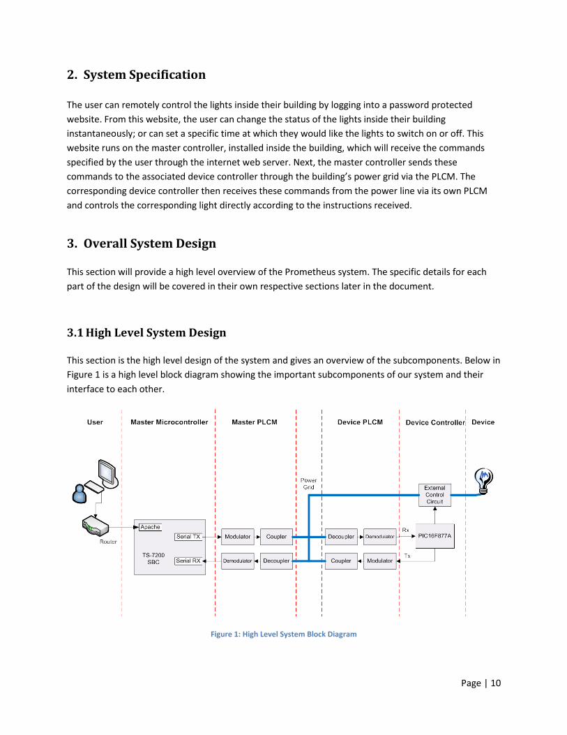
3.1 High Level System Design This section is the high level design of the system and gives an overview of the subcomponents. Below in Figure 1 is a high level block diagram showing the important subcomponents of our system and their interface to each other.
Figure 1: High Level System Block Diagram

Page | 11
The user communicates with the system through predefined commands on an internet website served by the master controller, and these commands are processed and translated into control signals to be sent out on the power grid. The commands will be modulated by the Power Line Communication Modem (PLCM) and coupled into the power line grid. On the device end, the signal will be decoupled, demodulated, and passed on to the device controller, responsible for controlling the targeted device. The device controller will then control the device through an external circuit. The device controller end of the system will consist of PIC microcontroller connected to the PLCM through its TX/RX pins [6], which will allow for RS232 communication from the master controller to the device controller. The PIC will use it I/O ports to control the corresponding device via external circuitry designed to provide electrical isolation between the PIC and the device, as well as sufficient power to the device.
3.2 Electrical Design In order to communicate with a device, the master controller sends data to the PLCM which is responsible for transmitting/receiving of the data signal over the power line. Each device that has to be controlled is also connected to a PLCM enabling it to communicate with the master controller. The reason why the PLCM has bidirectional communication is that after receiving the instructions from the master controller, the device controller should respond to the master controller and acknowledge whether the task was successfully accomplished or not. The PLCM consists of four stages to account for data communication over the power line: modulator circuit, coupling circuit, decoupling/signal conditioning circuit, and demodulation circuit. The design of all these circuits are explained thoroughly in section 5 of this. As mentioned above, the PIC will use its I/O ports to control a device via external circuitry. The external circuitry that connects the device controller to the device is necessary to protect the device controller itself and also the PLCM. The PIC will be connected to a high voltage/current circuit that will control and power a 120 VAC light bulb. Fuses will be necessary in our circuits to protect the circuitry within the device controller from power surges. We will make use of opto-isolators to optically isolate the high voltage signals from the device controller.
3.2.1 Power Supply Requirements The PLCM operates at Volts since operational amplifiers are used to provide RS232 voltage range within the system. The exact power rating required for the PLCM is still unknown as the design is not yet fully complete and assumptions cannot be made. The device controller will require both a +5 Volts reference voltage and a +15 Volts reference. The +5 voltage reference will be used to power up the PIC, and the +15 voltage reference will be used for the external circuitry. The total power usage of the device controller is as well unknown at this point as the circuit is still in the implementation stage.
Page | 12
3.3 Mechanical Design
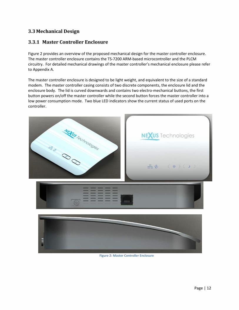
3.3.1 Master Controller Enclosure Figure 2 provides an overview of the proposed mechanical design for the master controller enclosure. The master controller enclosure contains the TS-7200 ARM-based microcontroller and the PLCM circuitry. For detailed mechanical drawings of the master controller’s mechanical enclosure please refer to Appendix A. The master controller enclosure is designed to be light weight, and equivalent to the size of a standard modem. The master controller casing consists of two discrete components, the enclosure lid and the enclosure body. The lid is curved downwards and contains two electro-mechanical buttons, the first button powers on/off the master controller while the second button forces the master controller into a low power consumption mode. Two blue LED indicators show the current status of used ports on the controller.
Figure 2: Master Controller Enclosure
Page | 13
The enclosure lid is mounted onto the enclosure body through the use of screws. The enclosure body contains mounting holes for the Ethernet port and power port. The enclosure body features venting on its back side for heat dissipation purposes. Without considering electrical components, the table below lists the master controller’s enclosure maximum dimensions and weight information.
Table 1: Master Controller Enclosure Properties
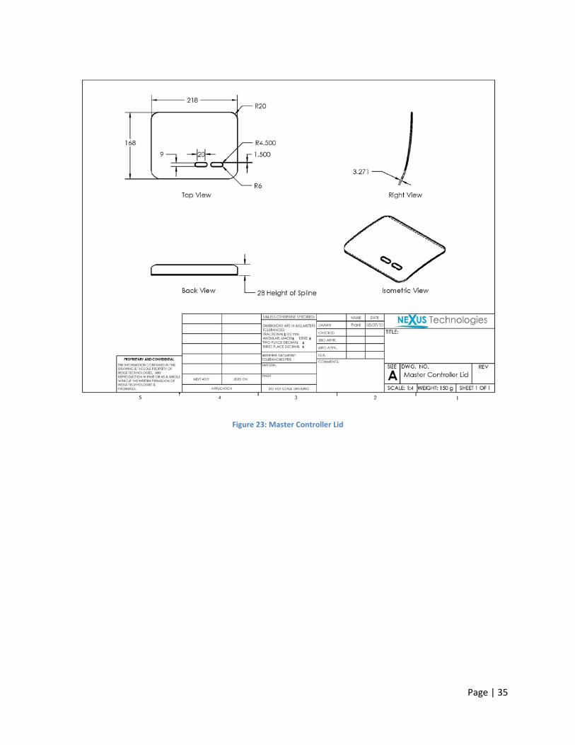
For more detailed dimensions for the enclosure please refer to the master controller’s enclosure body and lid mechanical drawings in Appendix A.
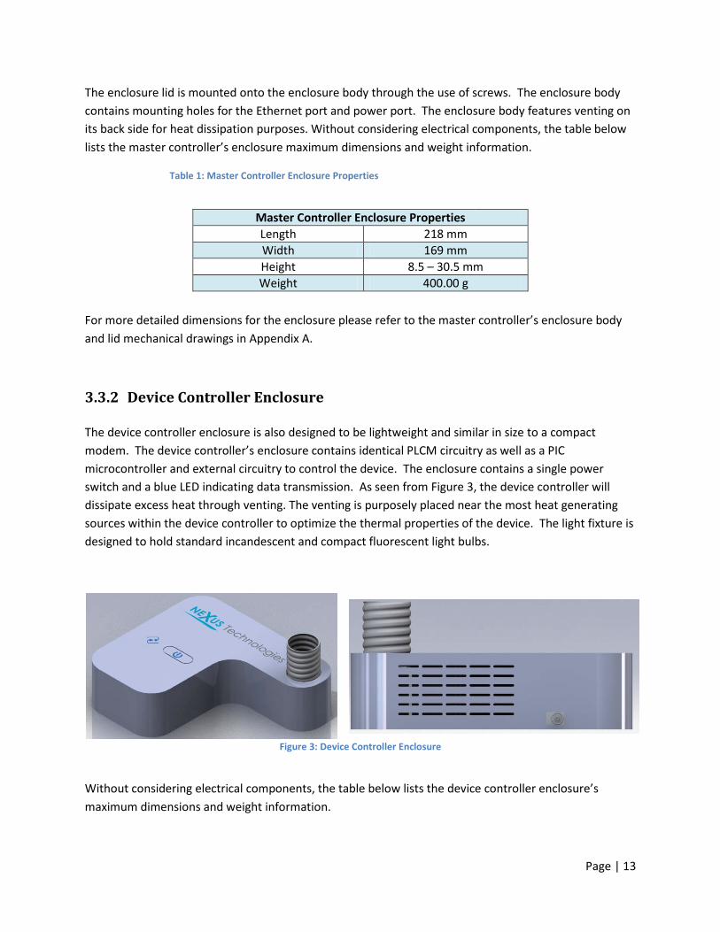
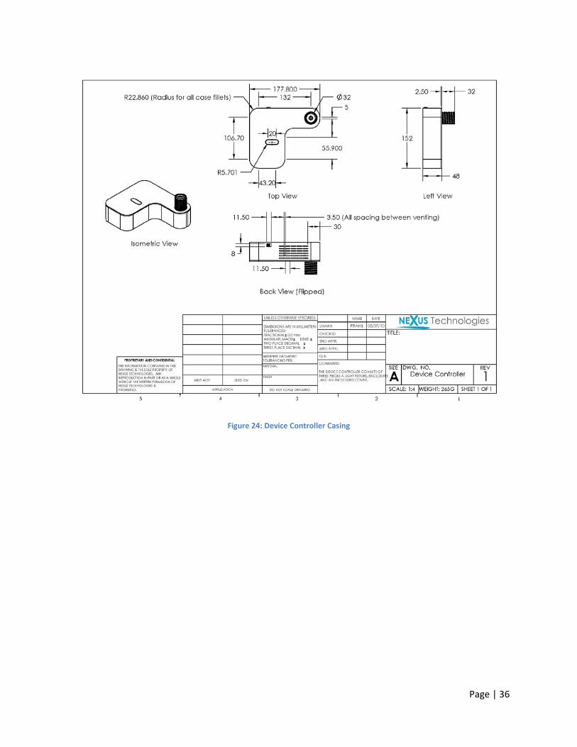
3.3.2 Device Controller Enclosure The device controller enclosure is also designed to be lightweight and similar in size to a compact modem. The device controller’s enclosure contains identical PLCM circuitry as well as a PIC microcontroller and external circuitry to control the device. The enclosure contains a single power switch and a blue LED indicating data transmission. As seen from Figure 3, the device controller will dissipate excess heat through venting. The venting is purposely placed near the most heat generating sources within the device controller to optimize the thermal properties of the device. The light fixture is designed to hold standard incandescent and compact fluorescent light bulbs.
Figure 3: Device Controller Enclosure
Without considering electrical components, the table below lists the device controller enclosure’s maximum dimensions and weight information.
Master Controller Enclosure Properties Length 218 mm Width 169 mm Height 8.5 – 30.5 mm Weight 400.00 g

Page | 14
Table 2: Device Controller Enclosure Properties
For more detailed dimensions for the enclosure please refer to the device controller mechanical drawing in Appendix A.
4. Master Controller Design
4.1 Purpose The purpose of the master controller is to provide an interface between the user and the Prometheus system, as well as provide overall control of the system. The master controller, illustrated in Figure 4, consists of a TS-7200 Single Board Computer (SBC) purchased from Technologic Systems.
Figure 4: TS-7200 SBC
Device Controller Enclosure Properties Length 106.7 mm Width 177.8 mm Height 48.0 mm Weight 265.0 g
Page | 15
The processor on the TS-7200 SBC is an ARM 9 processor which operates at 200MHz, and has 32MB of high speed DDR RAM. Debian Linux V2.6 is installed on a 2GB compact flash card, and is loaded on boot-up by manually interrupting the Redboot boot loader program. The user web interface will be provided by an Apache web server included in the Linux operating system. A terminal interface is provided by the COM1 serial port, and the COM2 serial port will be used for communication between the master controller and the device controller. Please see Appendix B for more information regarding the operation of the master controller.
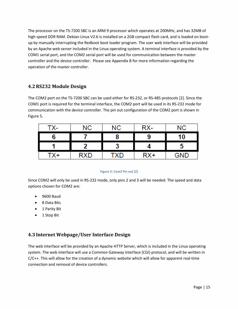
4.2 RS232 Module Design The COM2 port on the TS-7200 SBC can be used either for RS-232, or RS-485 protocols [2]. Since the COM1 port is required for the terminal interface, the COM2 port will be used in its RS-232 mode for communication with the device controller. The pin out configuration of the COM2 port is shown in Figure 5.
Figure 5: Com2 Pin out [2]
Since COM2 will only be used in RS-232 mode, only pins 2 and 3 will be needed. The speed and data options chosen for COM2 are:
• 9600 Baud
• 8 Data Bits
• 1 Parity Bit
• 1 Stop Bit
4.3 Internet Webpage/User Interface Design The web interface will be provided by an Apache HTTP Server, which is included in the Linux operating system. The web interface will use a Common Gateway Interface (CGI) protocol, and will be written in C/C++. This will allow for the creation of a dynamic website which will allow for apparent real-time connection and removal of device controllers.
Page | 16
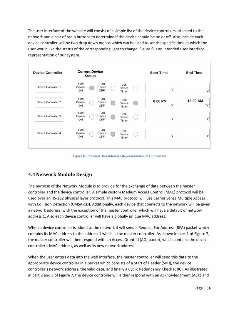
The user interface of the website will consist of a simple list of the device controllers attached to the network and a pair of radio buttons to determine if the device should be on or off. Also, beside each device controller will be two drop down menus which can be used to set the specific time at which the user would like the status of the corresponding light to change. Figure 6 is an intended user interface representation of our system.
Start Time End TimeDevice Controller Current Device Status
Device Controller 1Turn
Device ON VV
Use Device Timer
Device Controller 2Turn
Device ON
12:00 AMV
6:00 PMV
Use Device Timer
Device Controller 3Turn
Device ON VV
Use Device Timer
Device Controller 4Turn
Device ON VV
Use Device Timer
Turn Device OFF
Turn Device OFF
Turn Device OFF
Turn Device OFF
Figure 6: Intended User Interface Representation of Our System
4.4 Network Module Design The purpose of the Network Module is to provide for the exchange of data between the master controller and the device controller. A simple custom Medium Access Control (MAC) protocol will be used over an RS-232 physical layer protocol. This MAC protocol will use Carrier Sense Multiple Access with Collision Detection (CMSA-CD). Additionally, each device that connects to the network will be given a network address, with the exception of the master controller which will have a default of network address 1. Also each device controller will have a globally unique MAC address. When a device controller is added to the network it will send a Request For Address (RFA) packet which contains its MAC address to the address 1 which is the master controller. As shown in part 1 of Figure 7, the master controller will then respond with an Access Granted (AG) packet, which contains the device controller’s MAC address, as well as its new network address. When the user enters data into the web interface, the master controller will send this data to the appropriate device controller in a packet which consists of a Start of Header (SoH), the device controller’s network address, the valid data, and finally a Cyclic Redundancy Check (CRC). As illustrated in part 2 and 3 of Figure 7, the device controller will either respond with an Acknowledgment (ACK) and
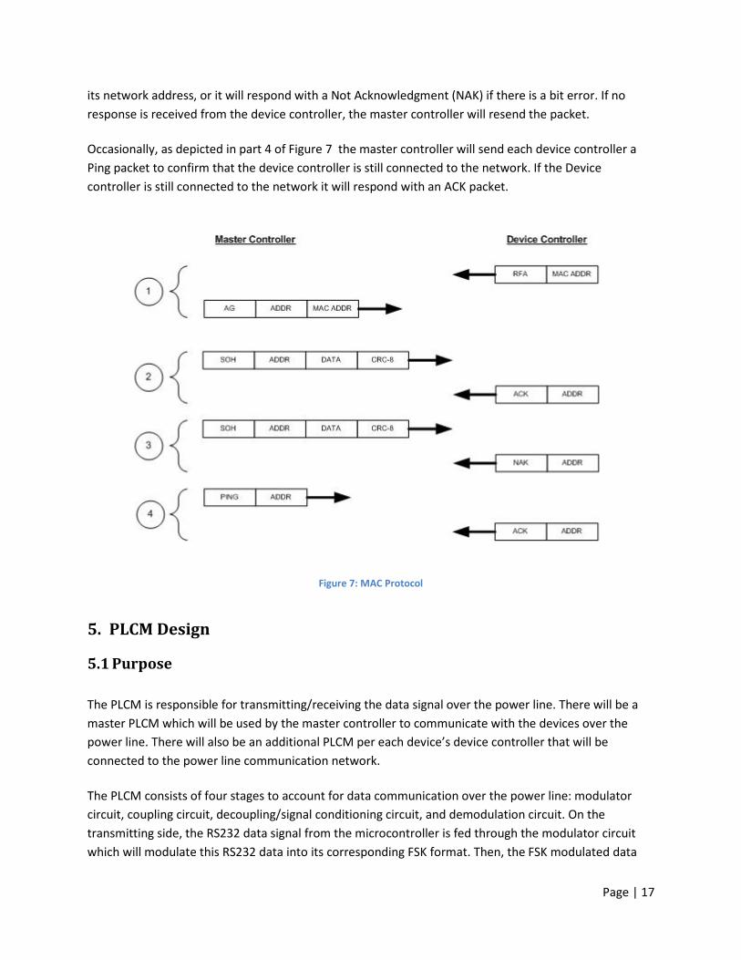
Page | 17
its network address, or it will respond with a Not Acknowledgment (NAK) if there is a bit error. If no response is received from the device controller, the master controller will resend the packet. Occasionally, as depicted in part 4 of Figure 7 the master controller will send each device controller a Ping packet to confirm that the device controller is still connected to the network. If the Device controller is still connected to the network it will respond with an ACK packet.
Figure 7: MAC Protocol
5. PLCM Design
5.1 Purpose
The PLCM is responsible for transmitting/receiving the data signal over the power line. There will be a master PLCM which will be used by the master controller to communicate with the devices over the power line. There will also be an additional PLCM per each device’s device controller that will be connected to the power line communication network. The PLCM consists of four stages to account for data communication over the power line: modulator circuit, coupling circuit, decoupling/signal conditioning circuit, and demodulation circuit. On the transmitting side, the RS232 data signal from the microcontroller is fed through the modulator circuit which will modulate this RS232 data into its corresponding FSK format. Then, the FSK modulated data

Page | 18
signal is fed through the coupling circuit to be superimposed onto the AC power line signal. On the receiving side, the FSK modulated signal is extracted from the power line through the decoupling circuitry, and demodulated back into its RS232 data format via the demodulator circuit. More detailed design description of each stage of the PLCM is described in the remainder of this section.
5.2 Modulator Circuit Design The main purpose of the modulator circuit is to modulate the RS232 data coming from the transmitting microcontroller in the FSK format to be ready for transmission over the power line grid. The reason we chose the FSK modulating format is because it is much more immune to noise in comparison with other modulating methods such as amplitude modulation (AM). Aside from unpredictable noise present on the power line grid, there are also unknown power line characteristics and fluctuations in the power-line impedance level as appliances are continuously switched in and out of the grid. Therefore, dependence on the amplitude of the modulating signal would not be the most reliable method for transmission of signal over the power line grid. Moreover, with the use of the FSK method, the modulating frequencies can be set for much higher than the 60 Hz 120-Volt power signal to allow for easy distinction of the modulated signal from the power signal with just the use of a band-pass filter. Lastly, FSK modulation is easily achieved with just the use of a VCO, which has a linear relationship between its input voltage and its output frequency. Please refer to Figure 8 for an example of an RS232 data signal and its corresponding FSK modulated signal. As can be seen from the figure, an RS232 logic “0” (+15 Volts) is modulated into a 15 Volts pk-pk signal of frequency f_hig, and an RS232 logic “1” (-15 Volts) into a 15 Volts pk-pk signal of frequency f_low.
RS 232 data from the microcontroller
-15 Volts
+15 Volts
010 1 01
+15 Volts
0 Volts
The corresponding FSK modulated signal
f_high f_low f_low f_high f_low f_high
Figure 8: An Example of an RS232 Data Signal and Its Corresponding FSK Modulated Signal

Page | 19
To achieve an FSK modulated signal, our circuit was built around the VCO provided in the CD4046 IC chip. The design was aimed to provide a 439 kHz, 15-Volt pk-pk signal for an RS232 logic “0” and a 357 kHz, 15-Volt pk-pk signal for an RS232 logic “1”. Please refer to Figure 9 for the complete circuit diagram of the FSK modulator. The RS232 data coming in from the microcontroller is initially passed through a clipper circuit consisting of R10 and D1 to shift the -15 Volts representing an RS232 logic “1” to 0 Volts as the CD4046 cannot operate at any negative voltages. Hence, a logic “1”, is seen as 0 Volts to the CD4046.
Figure 9:FSK Modulator Circuit
The remainder of the circuitry built around the CD4046 IC is obtained through its datasheet of the. The design procedure is as follows:
a. The f_max value representing an RS232 logic “0” and the f_min value representing an RS232 logic “1” are chosen. In our case f_max = 439 kHz, and f_min = 357 kHz. The reason we chose them to be such high values is because they can be easily distinguished from the 60 Hz AC power signal.
b. Knowing the f_min value, R2 and C1 are obtained from Figure 10 below [3]. In our case, we
obtained R2 and C1 to be 10 kΩ and 500 pF, respectively.

Page | 20
Figure 10: Graph for Obtaining the Values of C1 and R2 Given the Value of f_min [3]
c. Having obtained the R2, f_mix, and f_min values, the value of R1 is found using Figure 11 below [3]. We obtained R1 to be 22 kΩ for our case.
Figure 11:Graph Showing the Ratio of R2 over R1, Given the Ratio of f_max and f_min [3]
The relationship between the input voltage and the output frequency of our FSK circuit is shown below in Figure 12.

Page | 21
Figure 12: The Relationship between the VCO Input Voltage and the Output Frequency
5.3 Coupling Circuit Design The coupling circuit is responsible for superimposing the FSK modulated data signal onto the AC power line signal for transmission over the power line grid. The coupling circuit can be viewed as a filter that passes the high frequency data signal while rejecting the low frequency power line signal. In order to successfully choose the appropriate component values to couple the FSK modulated data signal onto the power line, one should note that the signal on the power line has a high voltage and low frequency, while the modulated FSK signal has a low voltage and high frequency. Coupling capacitors, coupling transformers, and blocking inductors are used for the implementation of the coupling circuitry [4], [5]. The FSK signal passes through coupling capacitors of small value which act as a high pass filter, rejecting the power line signal. Therefore, coupling capacitors should be able to withstand being exposed to high voltage signals. Consequently, these capacitors should be designed to handle high frequency signals. Coupling transformers are used to provide galvanic isolation, impedance matching, voltage or current transformation, and filtering [4], [5]. The power line signal has a low frequency and high voltage, and it could have a saturation effect of at least 105 compared to the FSK signal. Thus, before entering the
coupling transformer, the power line signal should be first filtered by ≈ 100 dB [4]. Blocking inductors are used to prevent the inductor of the coupling transformer from getting saturated [4], [5]. These inductors can also be used to change the bandwidth of the band pass filter explained in the following paragraphs. A coupling transformer has a “leakage” inductance which can be considered as the coupling transformer’s internal impedance. Therefore, every coupling transformer has a low-pass filtering effect.

Page | 22
The coupling circuit, however, is also required to have band-pass filter features for filtering out the power line signals with low frequencies and prevent the coupling transformer from getting saturated. Hence, a capacitor should also be placed in series with the primary terminal of the coupling transformer [4]. The series capacitor, leakage transformer, and the resistive load construct a band pass filter of order two [4]. The center frequency of this band pass filter can be obtained from equation 1. In addition, the low and high cut-off frequencies can be calculated from equations 2 and 3, respectively [4].
(1)
(2)
(3)
Figure 13 below illustrates an example of a coupling circuit discussed above. A GDE25-1 high frequency transformer from Triad Magnetics was used as the coupling transformer.
Figure 13: Example of a Coupling Circuit [4]
5.4 Decoupling/Signal Conditioning Circuit Design On the receiving side, the PLCM must first decouple the FSK modulated signal from the AC power line to then have it demodulated into its RS232 format. Since the FSK signal will be rather distorted after decoupling it from the power line, it also needs to be modified to take the shape of a square wave with the correct amplitude before being fed to the demodulator. Since coupling and decoupling of the FSK signal is virtually the same other than the direction of the signal flow, the design considerations needed for the decoupling circuitry are exactly the same as the coupling circuitry explained in section 5.2.

Page | 23
As for the signal conditioning of the FSK signal after decoupling has taken place, we must first amplify the decoupled signal followed by passing it through a pulse shaper before proceeding with the demodulation stage. The amplification stage will consist of a simple op-amp circuit which will take the decoupled signal and multiply it by a constant gain. The pulse shaper will be a comparator circuit which will ensure that the signal is a square wave signal with 0V to +15V range.
5.5 Demodulator Circuit Design The purpose of the demodulator is to take the FSK modulated signal which has been decoupled from the power line and convert it into its corresponding RS232 format. This reconfigured RS232 signal will then be passed onto the microcontroller for data interpretation. The demodulation is done through the use of a PLL which consists of a phase comparator, a source follower and a VCO. The PLL is explained in more details in below. A CD4046 IC PLL was used to demodulate the FSK signal back into its corresponding RS232 data format. See Figure 14 for the general block diagram of the PLL.
Figure 14: PLL General Block Diagram
The phase comparator produces an output which is proportional to the phase difference between the input FSK signal and the VCO output frequency. The output is then passed on through a low pass filter, producing an average error voltage which is applied to the VCO. This error voltage produces a change in the VCO frequency which moves it closer to the FSK input frequency. Once the FSK input signal frequency and the VCO frequency are equal, the PLL is now said to be locked on to the input frequency. The error voltage now indicates the data level. The final circuit for the PLL demodulator is shown below in Figure 15.
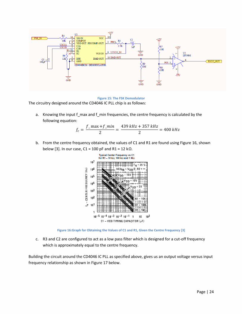
Page | 24
Figure 15: The FSK Demodulator The circuitry designed around the CD4046 IC PLL chip is as follows:
a. Knowing the input f_max and f_min frequencies, the centre frequency is calculated by the following equation:
b. From the centre frequency obtained, the values of C1 and R1 are found using Figure 16, shown
below [3]. In our case, C1 = 100 pF and R1 = 12 kΩ.
Figure 16:Graph for Obtaining the Values of C1 and R1, Given the Centre Frequency [3]
c. R3 and C2 are configured to act as a low pass filter which is designed for a cut-off frequency which is approximately equal to the centre frequency.
Building the circuit around the CD4046 IC PLL as specified above, gives us an output voltage versus input frequency relationship as shown in Figure 17 below.

Page | 25
Figure 17: The PLL Output Voltage versus Its Input Frequency Relationship Obtained
As shown in Figure 17 above, for f_min of 357 kHz (RS232 logic “1”) and f_max of 439 kHz (RS232 logic “0”) the PLL’s output voltages are 6.70 Volts and 8.22 Volts, respectively. Since for means of RS232 communication, we need the voltages to be -15 Volts for a logic “1” and +15 Volts for a logic “0”, the output of the PLL is passed on to a comparator ,U3 in the circuit diagram, to adjust for this shifting required in the output voltage levels.
5.6 Safety Issues Safety plays a major role in our project as we are dealing with a mixture of high AC voltages and low DC voltages in our circuits. We must ensure none of the high voltage from the power line grid passes through to the low voltage DC side to prevent any possible damages to our components. Even though, our circuits are designed in such a way to filter out the AC signal before getting anywhere close to the DC operating components, our final product will include extra safety features in case of component break down. One of the major methods of adding more safety to our design is to make use of opto-isolators, for isolating the high voltage side of the circuits from the low voltage side. With the use of opto-isolators, in case of a power surge, the worst thing which could happen is that the opto-isolators itself will burn out as it optically isolates one side of the circuit from the other. Another component which we will make use of for adding safety will be fuses. Fuses will be installed on the input receiving and the output transmitting sides to prevent any high voltage signals from over driving the components.
Page | 26
6. Device Controller Design
6.1 Purpose The device controller is required to communicate with the master controller and in regards to controlling the corresponding device connected to it. The device controller needs to be cheap, power efficient, and capable of handling communications with the master controller and controlling the required device. The device controller will need to receive and transmit RS232 data through the PLCMs and control a device using external circuitry connected to its I/O ports. The most cost efficient choice that can handle the processing requirements and the one we have chosen is a PIC microcontroller.
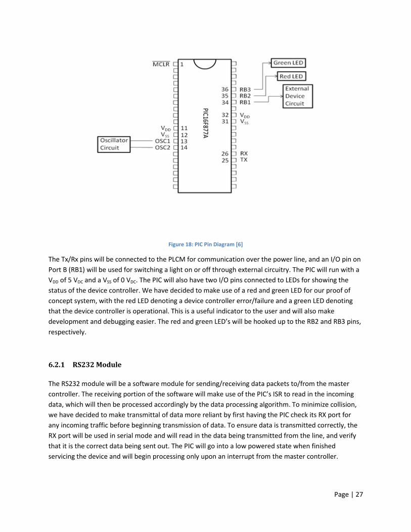
6.2 PIC Design We have chosen the PIC16F877A 8 bit microcontroller as it has enough processing power and memory to run a single threaded program with an Interrupt Service Routine (ISR) which is enough to handle communications with the master controller. We do not require any accurate calculations, so a 16 bit controller is unnecessary for the device controller end. The communications will be done through RS232 and will make use of the PIC’s USART and Tx/Rx pins. The PIC operates at 4 MHz and contains 8 kB of flash memory in addiction to I/O ports which will be used for controlling of the device and status indication. We have chosen a 4 MHz clock to prevent over driving the PIC’s internal hardware, eventhough it can handle up to a 20 MHz clock frequency. Also, 4 MHz is fast enough to process the serial communication needed for our system. This clock signal must be provided by an external circuit containing a 4MHz clock crystal, and connected to the clock pins of the PIC [6]. Below in Figure 18 is the pin diagram of the PIC and the external circuitry that needs to be connected to it. Only important pins are labelled in this figure. The details of the external device circuitry will be specified in section 6.3.
Page | 27
Figure 18: PIC Pin Diagram [6]
The Tx/Rx pins will be connected to the PLCM for communication over the power line, and an I/O pin on Port B (RB1) will be used for switching a light on or off through external circuitry. The PIC will run with a VDD of 5 VDC and a VSS of 0 VDC. The PIC will also have two I/O pins connected to LEDs for showing the status of the device controller. We have decided to make use of a red and green LED for our proof of concept system, with the red LED denoting a device controller error/failure and a green LED denoting that the device controller is operational. This is a useful indicator to the user and will also make development and debugging easier. The red and green LED’s will be hooked up to the RB2 and RB3 pins, respectively.
6.2.1 RS232 Module The RS232 module will be a software module for sending/receiving data packets to/from the master controller. The receiving portion of the software will make use of the PIC’s ISR to read in the incoming data, which will then be processed accordingly by the data processing algorithm. To minimize collision, we have decided to make transmittal of data more reliant by first having the PIC check its RX port for any incoming traffic before beginning transmission of data. To ensure data is transmitted correctly, the RX port will be used in serial mode and will read in the data being transmitted from the line, and verify that it is the correct data being sent out. The PIC will go into a low powered state when finished servicing the device and will begin processing only upon an interrupt from the master controller.

Page | 28
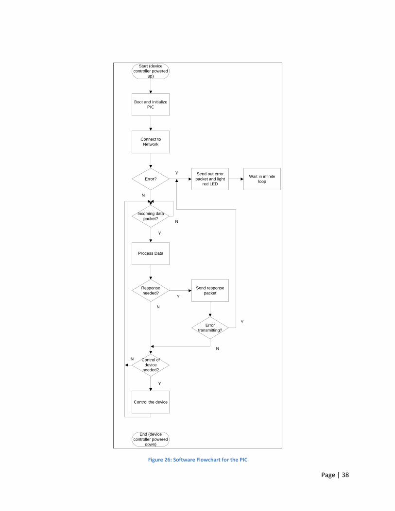
If an error occurs during the operation, the PIC will attempt to recover from the error. If the PIC is unsuccessful in recovering from the error, it will turn on the red LED for error indication and send an error packet to the master controller. We will aim to implement as much error handling as possible for the PIC, given its limited program space. Appendix B is a flowchart giving a general overview of the PIC’s software flow.
6.2.2 Signal Handling The PIC will communicate with the device using its I/O ports. For our proof of concept system, we will make use of one I/O pin (RB1) for device control as we will only be switching lights either on or off, but in our final product system, we may need to make use of more I/O pins as the devices to be controlled will require more complexity. The voltage and current output from the pin is not enough itself to control a 120 VAC light, so an external circuitry will be used to make sure the PIC is safely isolated from the high voltage light and able to provide the required current to the switching circuit. The green LED on RB3 will be turned on upon successful boot up of the PIC and connection to the master controller. Successful connection to the master controller will consist of the PIC introducing itself to the master controller by sending its MAC address. The PIC will then wait an ACK packed from the master controller with a network address, to be used for further communication.
6.3 Hardware Design The hardware section of the device controller consists of three parts. The first part is the external crystal oscillator circuit to provide the switching signal required for the clock input of the PIC. We have decided on using a 4 MHz clock, so a 4 MHz clock crystal will be used for this purpose. The clock circuit will be constructed as shown below in Figure 19.
Figure 19: PIC External Clock Circuit
This circuit is necessary as the PIC contains internal clock circuitry that requires this specific external circuit. From the PIC’s datasheet, a 4 MHz clock crystal requires capacitor values of 15 pF [6]. The second part of the hardware side of the device controller is for indicating the current status of the device controller. We will make use of two LEDs for this status indication which will be hooked up to the

Page | 29
RB2 and RB3 pins of the PIC. Each LED will have a current limiting resistance connected to it in series. The indication circuitry is shown below in Figure 20.
Figure 20:LED Circuit for PIC
The third part of the hardware circuitry is for controlling the corresponding device. This control circuitry will be designed to provide the sufficient power required for switching on/off the corresponding 120 V light bulb and will also ensure protection of the PIC by optically isolating the power circuitry from the PIC’s I/O pins. The opto-isolator will be driven by the PIC’s I/O pin and its output will be connected to a power MOSFET to provide a much higher current needed for switching a 120 VAC relay which will control the corresponding light bulb. The relay will require approximately 1-2 A, which is much higher than what the PIC could possibly provide. The relay will be triggered by the 1-2 A current, which will cause an inductive loop to generate a magnetic field to close the switch between the power source and light bulb. The control circuitry is shown below in Figure 21.
Figure 21: External Circuit for Light Control
The voltage VM will be the voltage required by the power MOSFET to supply the necessary switching current needed to operate the relay.

Page | 30
7. System Test Plan
7.1 Master Controller Unit Tests
7.1.1 Master Controller Web Interface Test User Input:
The user will select two devices connected within the network to turn on through the web interface. The user will then use the web interface to turn the two devices back off.
Conditions:
The master controller is not connected to the PLCM, and is running a simple CGI program which will assume that two device controllers are connected, and will output all user actions to the terminal.
Expected Observation:
This test will verify the functionality of the web interface, by outputting the user’s actions to the terminal. The terminal output should show two devices turning on, and then two devices turning off.
7.1.2 Master Controller RS-232 Test User Input:
None.
Conditions:
The master controller is not connected to the PLCM, but is instead connected to a computers serial port. The computer is running a C program which will emulate a device controller being connected to the network. The master controller is a will add the device controller to the network, and send it a sample data packet. The C program on the computer will display to the screen all communication packets sent to and received from the master controller.
Expected Observation:
This test will verify the functionality of the serial interface, by outputting the master controller’s actions to the terminal. The terminal output should show outputs corresponding to Figure 7.
7.2 PLCM Unit Tests
7.2.1 PLCM Unit Test 1: Modulator Circuit User Input:
None.

Page | 31
Conditions:
Instead of an RS232 signal a square wave is generated using a function generator to connect to the input pin of the modulator. A scope probe is connected to the output pin of the modulator.
Expected Observation:
The FSK signal with the desired frequencies i.e. 357 kHz corresponding to input data “1” or 439 kHz corresponding to input data “0” should appear on the oscilloscope monitor.
7.2.2 PLCM Unit Test 2: Demodulator Circuit User Input:
None.
Conditions:
A square signal with a desired frequency, i.e. 357 kHz or 439 kHz, generated from a function generator is connected to the input port of the demodulator. The output port is connected to an oscilloscope.
Expected Observation:
The oscilloscope connected to the output port of the demodulator should display the correct voltage level depending on the frequency of the signal generated via the function generator.
7.2.3 PLCM Unit Test 3: Coupling and Decoupling Circuits User Input:
None.
Conditions:
A square wave generated via a function generator with the desired frequency is connected to the input port of the coupling circuit. The coupling circuit, then must successfully couple the signal onto the AC power line grid. The decoupling circuit is then connected to the power line grid to extract the data signal sent from the coupling side. Expected Observation:
The same signal fed to the input port of the coupling circuit should appear on the output port of the decoupling circuit.
Page | 32
7.3 Device Controller Unit Tests
7.3.1 Device Controller Unit Test 1: Control of device through I/O pin User Input:
None.
Conditions:
The device controller is not connected to the PLCM through its Tx/Rx ports and is loaded with a simple program which will set the I/O pins RB1, RB2, and RB3 high and then low every 5 seconds. The I/O pin RB1 used for output to the device is connected to the necessary external circuitry such that it can control a light, and RB2 and RB3 pins are connected to LED circuits.
Expected Observation:
This test will verify the functionality of the external circuitry on the output pins of the PIC. The light should switch on and off every 5 seconds, along with the LEDs.
7.3.2 Device Controller Unit Test 2: Receiving and Transmitting Data User Input:
None.
Conditions:
The device controller is disconnected from the external circuitry of the light and a current limiting resistor in series with an LED is placed on the RB1 pin. The Tx/Rx ports are connected to a serial port allowing for data to be transmitted between the PIC and a host PC. The PIC is loaded with a program which can receive and mirror back data over its Tx/Rx pins.
Expected Observations:
The PIC should be able to receive data from the host PC and transmit the same data back.
7.3.3 Device Controller Unit Test 3: Communication with Master Controller User Input:
None.
Conditions:
The device controller is connected to a host PC running a program emulating the master controller. The device controller has only a resistive load on its output pin. The PIC is loaded with the software to communicate with the master controller.

Page | 33
Expected Behaviour:
The device controller will initiate communication with the master controller and get added to the network. It will properly receive, process, and respond to commands sent from the master controller.
7.4 System Tests
7.4.1 System Test 1: Overall System Functionality User Input:
Any possible user inputs from GUI, as tested in the master controller unit tests.
Conditions:
The overall system, after completion of all unit tests, is fully connected and loaded with required software. The master controller is connected to a PLCM at one electrical outlet, and the device controller to a PLCM on another electrical outlet.
Expected Behaviour:
The device controller will initiate communication with the master controller and get added to its network. It will properly receive, process, and respond to commands sent from the master controller. The PLCMs will properly transmit/receive the data between the master and device controllers. The light bulb being controlled will be under the full control of the user.
8. Conclusion The design solutions to the proposed functional specifications of the Prometheus system have been described in this document. These design specifications will be followed as closely as possible during the development phase, though the right to modify the design as required to meet the functional specifications is reserved. This document will guide development and will also provide testing plans to ensure that the final product meets the required specifications and functionality.
Page | 34
Appendix A: Mechanical Drawings
Figure 22: Master Controller Mechanical Casing
Page | 35
Figure 23: Master Controller Lid
Page | 36
Figure 24: Device Controller Casing

Page | 37
Appendix B: Software Flow Chart
Figure 25: High Level Software Flowchart for the Master Controller
Page | 38
Start (device controller powered
up)
Boot and Initialize PIC
Wait in infinite loop
Connect to Network
Send out error packet and light
red LEDError?
Incoming data packet?
Process Data
Response needed?
Send response packet
Control of device
needed?
Control the device
End (device controller powered
down)
Error transmitting?
Y
N
Y
Y
Y
Y
N
N
N
N
Figure 26: Software Flowchart for the PIC

Page | 39
References
[1]Nexus Technologies, “Functional Specification for Smart House with Power Line Communication Network,” ENSC 305/440, Feb. 9, 2010. [Online]. Available: http://www.ensc.sfu.ca/~whitmore/courses/ensc305/. [Accessed: Mar. 11, 2010].
[2]Technologic Systems, “TS-7200 Hardware Manual,” 2010. [Online]. Available: http://www.embeddedarm.com/documentation/ts-7200-manual.pdf. [Accessed: Mar. 10, 2010].
[3]“Datasheet CD4046 - CMOS MICROPOWER PHASE-LOCKED LOOP - Texas Instruments,” July 2003. [Online]. Available: http://pdf1.alldatasheet.com/datasheet-pdf/view/26873/TI/CD4046.html. [Accessed: Mar. 8, 2010].
[4]P. A. Janse Van Rensburg , “ Effective Coupling for Power-Line Communications,” January 2008. [Online]. Available: http://ujdigispace.uj.ac.za:8080/dspace/bitstream/10210/2442/1/JanseVanRensburg_FullThesis.pdf. [Accessed: Mar. 8, 2011]. [5] O. Bilal, E. Liu, Y. Gao, and. T. Korhonen. “Design of Broadband Coupling Circuits for Power-line Communication.”[Online]. Available: http://www.isplc2004.unizar.es/OSAMA%20BILAL.pdf. [Accessed: Mar. 8, 2011]. [6]“PIC16F87XA Data Sheet,” Microchip PIC16F877A. [Online]. Available: http://ww1.microchip.com/downloads/en/DeviceDoc/39582b.pdf. [Accessed: Mar. 10, 2010]. [7] Triad Magnetics, “Switchmode / High Frequency Gate Drive Transformers.” [ Online]. Available: http://triadmagnetics.com/pdf/Page%2021.pdf. [Accessed: Mar. 11, 2010].