low temperature plasma technologies for advanced packaging ... · plasma etch reactor first ever...
TRANSCRIPT
Plasma-Therm Confidential©2017 All Rights Reserved
Low Temperature Plasma Technologies
for Advanced Packaging Applications
David Lishan
NCCAVS - Northern California Chapter AVSJoint User Group Meeting (CMP, PAG, & TFUG)
June 12, 2018
1
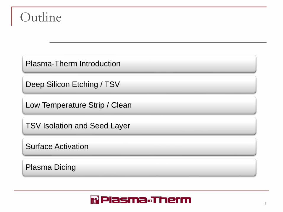
Outline
Plasma-Therm Introduction
Deep Silicon Etching / TSV
Low Temperature Strip / Clean
TSV Isolation and Seed Layer
Surface Activation
Plasma Dicing
2
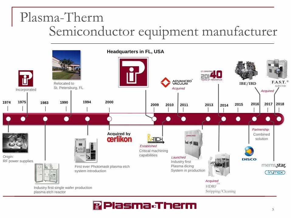
Relocated to
St. Petersburg, FL
1975 1990 20001974
Origin:
RF power supplies
Acquired by
2009
Industry first single wafer production
plasma etch reactor
First ever Photomask plasma etch
system introduction
1983 1994
Incorporated
Critical machining
capabilities
2010 2011 2013 2014
Plasma-ThermSemiconductor equipment manufacturer
2015
Industry first
Plasma dicing
System in production
HDRFTM
Stripping/Cleaning
2016
F.A.S.T. ®
ALD-CVD
2017
Headquarters in FL, USA
Combined
solution
Acquired
Partnership
Launched
AcquiredAcquired
Established
2018
IBE/IBD
3
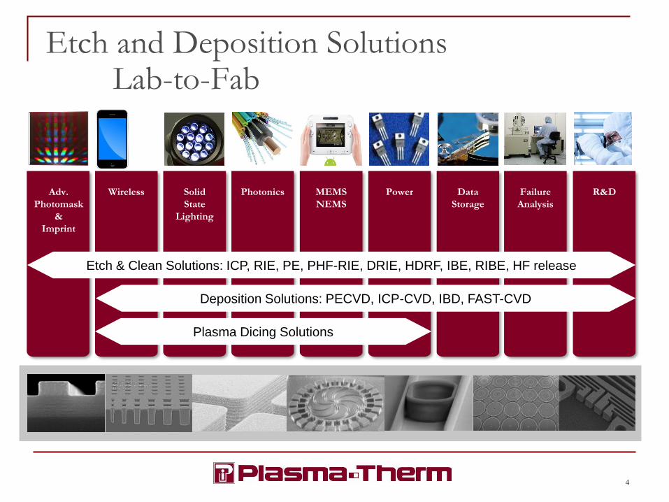
PowerAdv.
Photomask
&
Imprint
MEMS
NEMS
Solid
State
Lighting
PhotonicsWireless Data
Storage
Failure
Analysis
R&D
Etch and Deposition SolutionsLab-to-Fab
Etch & Clean Solutions: ICP, RIE, PE, PHF-RIE, DRIE, HDRF, IBE, RIBE, HF release
Deposition Solutions: PECVD, ICP-CVD, IBD, FAST-CVD
Plasma Dicing Solutions
4

Plasma Dicing
DEEP SILICON ETCHING / TSV
5
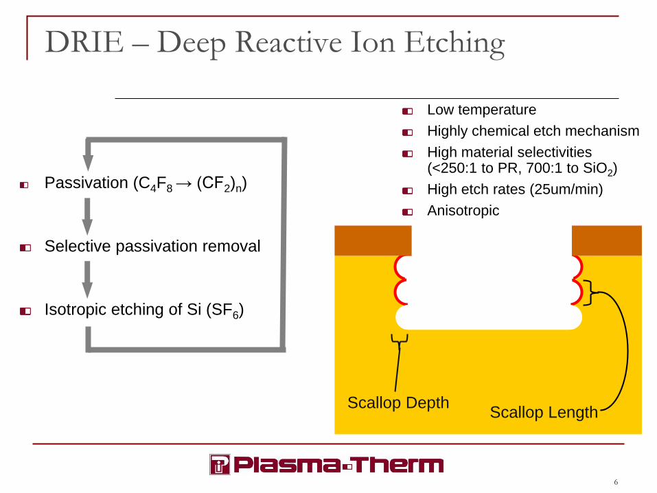
DRIE – Deep Reactive Ion Etching
Passivation (C4F8 → (CF2)n)
Scallop LengthScallop Depth
Low temperature
Highly chemical etch mechanism
High material selectivities(<250:1 to PR, 700:1 to SiO2)
High etch rates (25um/min)
Anisotropic
Isotropic etching of Si (SF6)
Selective passivation removal
6
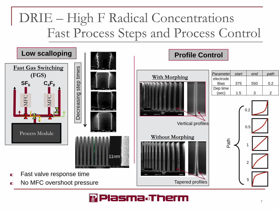
DRIE – High F Radical ConcentrationsFast Process Steps and Process Control
7
Process Module
C4F8SF6
MF
C
MF
C
Fast Gas Switching
(FGS)D
ecre
asin
g s
tep
tim
es
Tapered profiles
Vertical profiles
With Morphing
Without Morphing
Low scalloping Profile Control
0.2
0.5
1
2
5
Pa
th
Parameter start end path
electrode
Bias 375 550 0.2
Dep time
(sec) 1.5 3 2
Fast valve response time
No MFC overshoot pressure
11nm
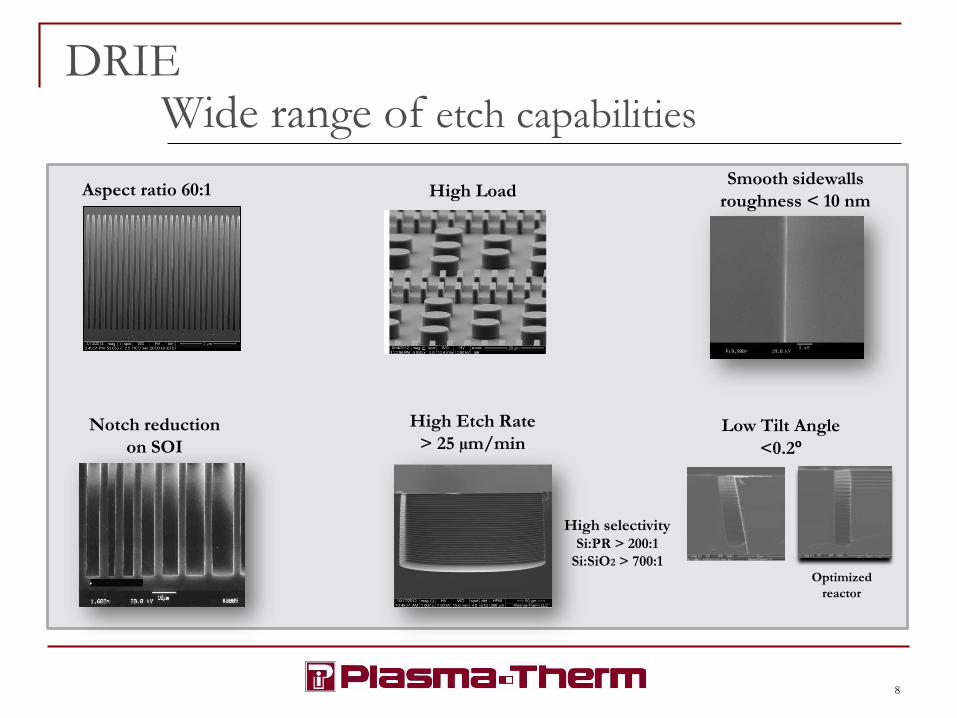
DRIEWide range of etch capabilities
8
Aspect ratio 60:1
High Etch Rate
> 25 µm/minLow Tilt Angle
<0.2º
Smooth sidewalls
roughness < 10 nmHigh Load
Notch reduction
on SOI
High selectivity Si:PR > 200:1
Si:SiO2 > 700:1Optimized
reactor
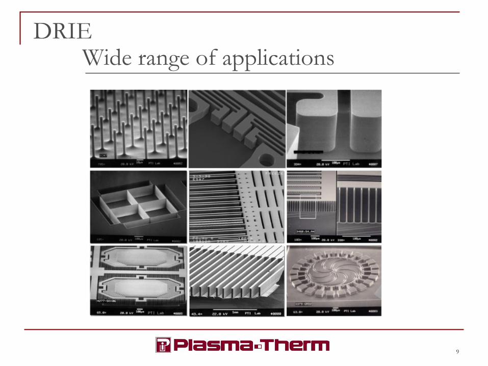
DRIE Wide range of applications
9
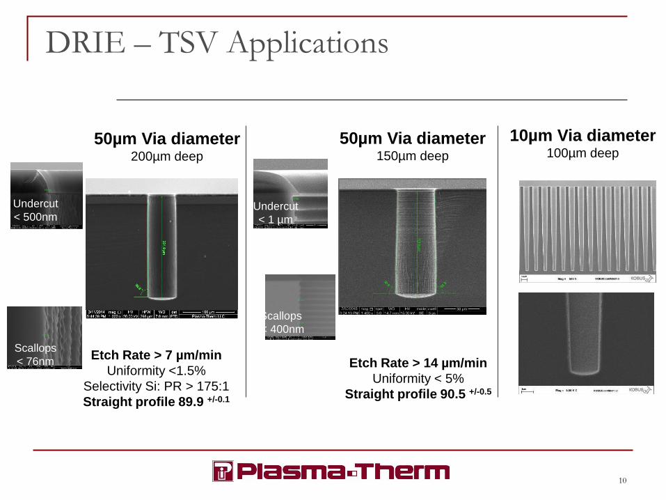
DRIE – TSV Applications
10
Etch Rate > 7 µm/min
Uniformity <1.5%
Selectivity Si: PR > 175:1
Straight profile 89.9 +/-0.1
50µm Via diameter200µm deep
Scallops
< 76nm
Undercut
< 500nm
Etch Rate > 14 µm/min
Uniformity < 5%
Straight profile 90.5 +/-0.5
50µm Via diameter150µm deep
Undercut
< 1 µm
Scallops
< 400nm
10µm Via diameter100µm deep
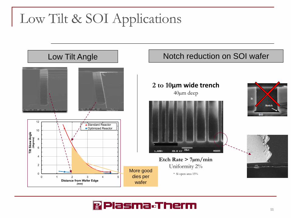
Low Tilt & SOI Applications
Etch Rate > 7µm/min
Uniformity 2%
* Si open area 15%
2 to 10µm wide trench40µm deep
Notch reduction on SOI waferLow Tilt Angle
More good
dies per
wafer
11
Plasma Dicing
LOW TEMPERATURE STRIP / CLEAN
12
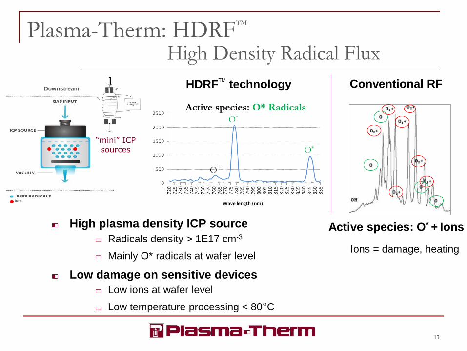
13
O*
O*
O+
HDRFTM
technology Conventional RF
Active species: O* Radicals
Active species: O* + Ions
Plasma-Therm: HDRFTM
High Density Radical Flux
Ions = damage, heating
Downstream
ions
High plasma density ICP source
Radicals density > 1E17 cm-3
Mainly O* radicals at wafer level
Low damage on sensitive devices
Low ions at wafer level
Low temperature processing < 80°C
“mini” ICPsources
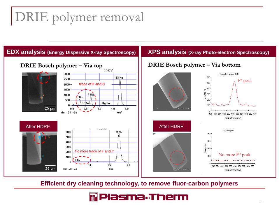
10KV
10KV
DRIE Bosch polymer – Via top DRIE Bosch polymer – Via bottom
F* peak
No more F* peak
DRIE polymer removal
EDX analysis (Energy Dispersive X-ray Spectroscopy)
No more trace of F and C
Efficient dry cleaning technology, to remove fluor-carbon polymers
After HDRF After HDRF
XPS analysis (X-ray Photo-electron Spectroscopy)
14
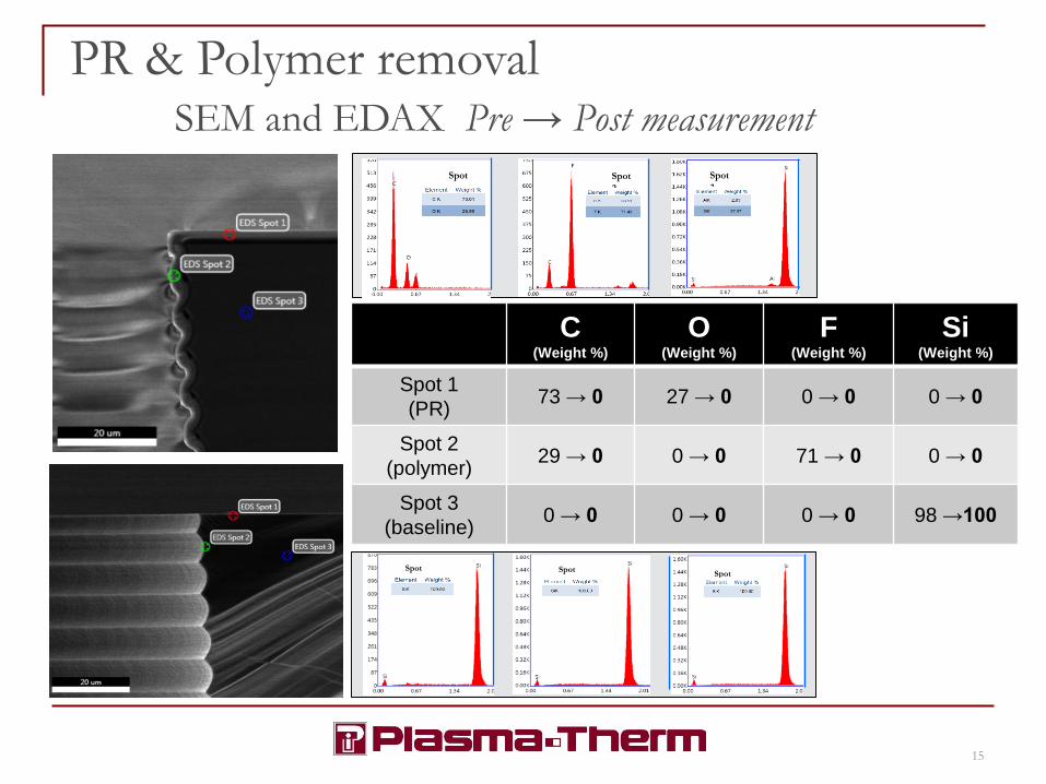
PR & Polymer removalSEM and EDAX Pre → Post measurement
Spot
1Spot
2
Spot
3
C(Weight %)
O(Weight %)
F(Weight %)
Si(Weight %)
Spot 1
(PR)73 → 0 27 → 0 0 → 0 0 → 0
Spot 2
(polymer)29 → 0 0 → 0 71 → 0 0 → 0
Spot 3
(baseline)0 → 0 0 → 0 0 → 0 98 →100
Spot
1Spot
2Spot
3
15
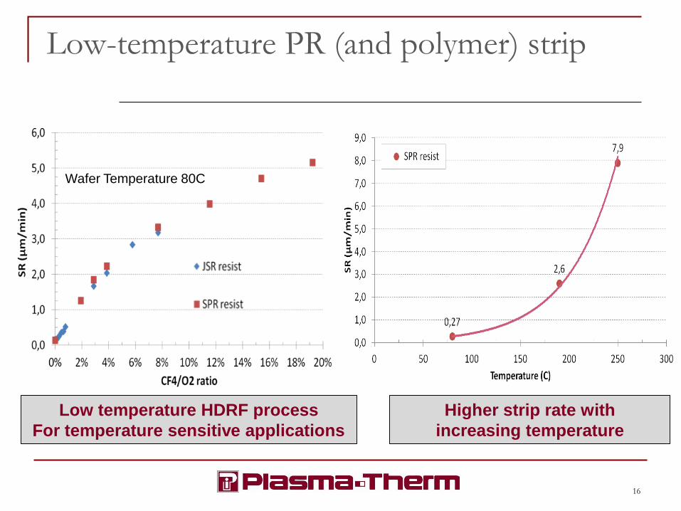
Low-temperature PR (and polymer) strip
Low temperature HDRF process
For temperature sensitive applications
16
Higher strip rate with
increasing temperature
Wafer Temperature 80C
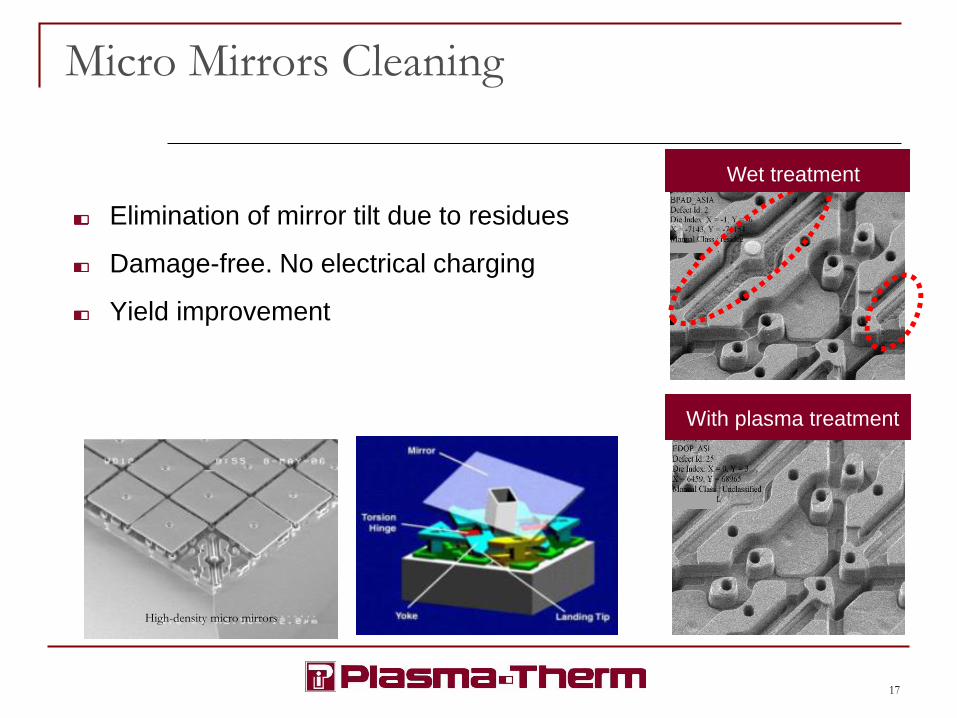
Micro Mirrors Cleaning
Elimination of mirror tilt due to residues
Damage-free. No electrical charging
Yield improvement
17
High-density micro mirrors
Wet treatment
With plasma treatment

Plasma Dicing
TSV ISOLATION and SEED LAYER
18
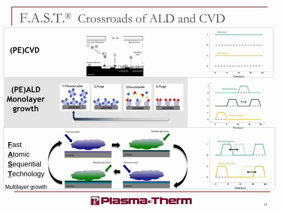
(PE)CVD
F.A.S.T.® Crossroads of ALD and CVD
19
(PE)ALD
Monolayer
growth
Fast
Atomic
Sequential
Technology
Multilayer growth
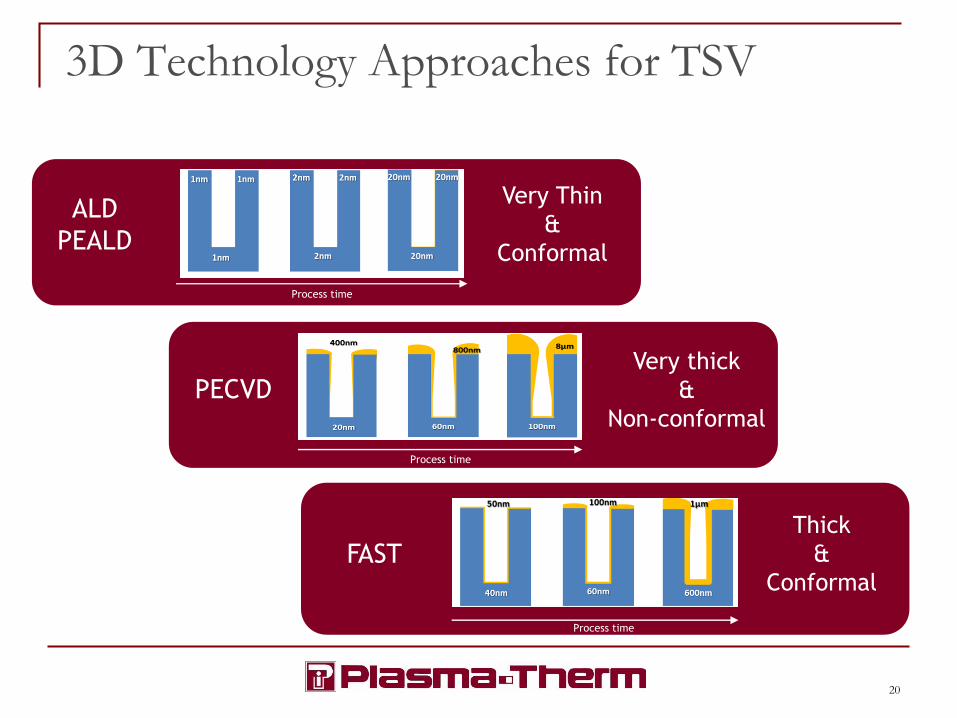
3D Technology Approaches for TSV
ALD
PEALD
Very Thin
&
Conformal
Process time
Process time
PECVDVery thick
&
Non-conformal
Process time
FASTThick
&
Conformal
20
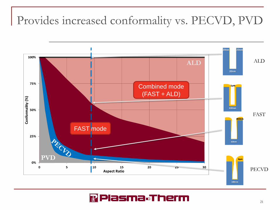
PVD
FAST mode
Combined mode
(FAST + ALD)
ALD
Provides increased conformality vs. PECVD, PVD
FAST
ALD
PECVD
21
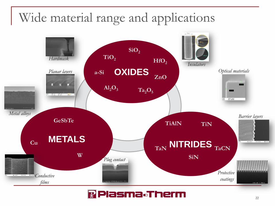
OXIDES
NITRIDESMETALS
Wide material range and applications
Metal alloys
Planar layers
HardmaskInsulators
Conductive
films
Optical materials
Barrier layers
Plug contact
SiO2
a-Si
Al2O3
ZnO
Ta2O5
TiO2 HfO2
Protective
coatings
SiN
TiAlN
TaCN
TiN
TaNW
Cu
GeSbTe
22
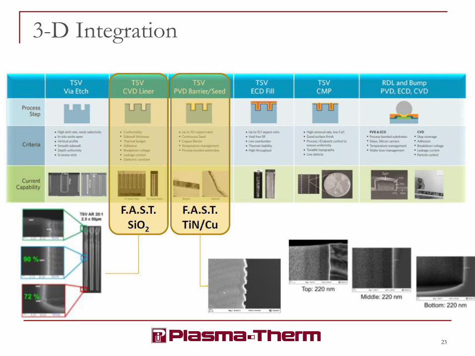
3-D Integration
23
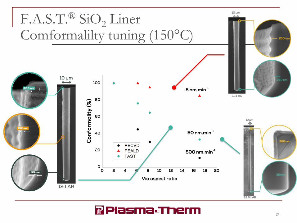
F.A.S.T.® SiO2 LinerComformalilty tuning (150°C)
24
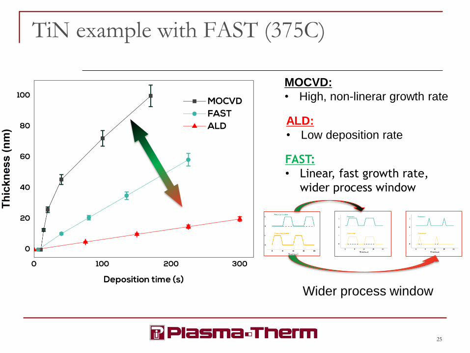
TiN example with FAST (375C)
25
MOCVD:
• High, non-linerar growth rate
ALD:
• Low deposition rate
FAST:
• Linear, fast growth rate,
wider process window
Wider process window
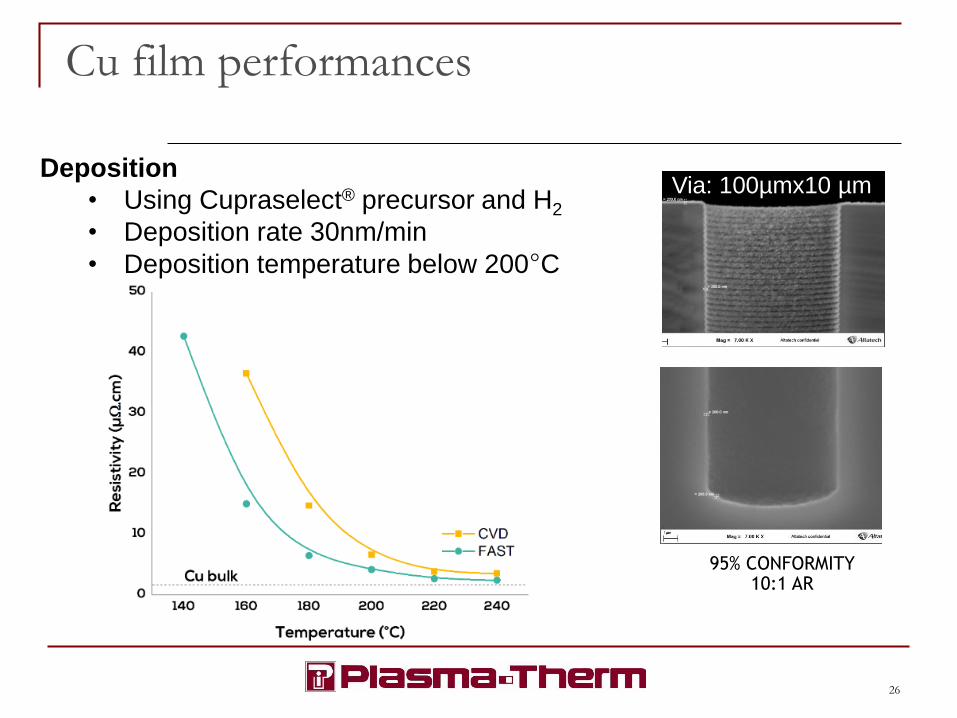
Cu film performances
26
95% CONFORMITY10:1 AR
Via: 100µmx10 µmDeposition
• Using Cupraselect® precursor and H2
• Deposition rate 30nm/min
• Deposition temperature below 200°C

Plasma Dicing
SURFACE ACTIVATION
27
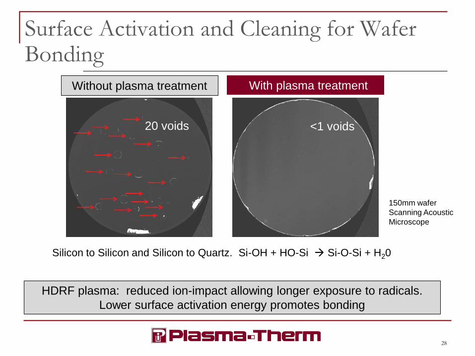
Surface Activation and Cleaning for Wafer Bonding
150mm wafer
Scanning Acoustic
Microscope
Without plasma treatment With plasma treatment
28
HDRF plasma: reduced ion-impact allowing longer exposure to radicals.
Lower surface activation energy promotes bonding
Silicon to Silicon and Silicon to Quartz. Si-OH + HO-Si → Si-O-Si + H20
20 voids <1 voids
High density radical plasma treatment
O2/Ar at 50°C
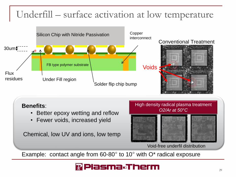
Copper
interconnect
Under Fill regionSolder flip chip bump
Silicon Chip with Nitride Passivation
Flux
residues
FB type polymer substrate
Benefits:
• Better epoxy wetting and reflow
• Fewer voids, increased yield
Chemical, low UV and ions, low temp
Underfill – surface activation at low temperature
Voids
Void-free underfil distribution
Conventional Treatment
Example: contact angle from 60-80° to 10° with O* radical exposure
30um
29
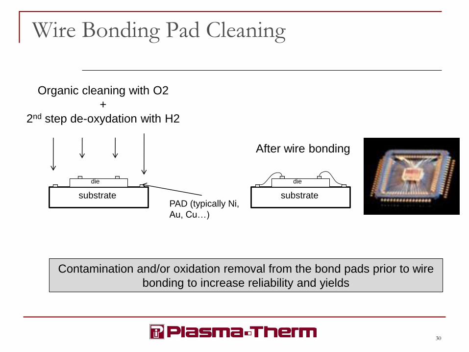
Organic cleaning with O2
+
2nd step de-oxydation with H2
Contamination and/or oxidation removal from the bond pads prior to wire
bonding to increase reliability and yields
PAD (typically Ni,
Au, Cu…)
After wire bonding
substrate
die
substrate
die
Wire Bonding Pad Cleaning
30
Plasma Dicing
PLASMA DICING
31
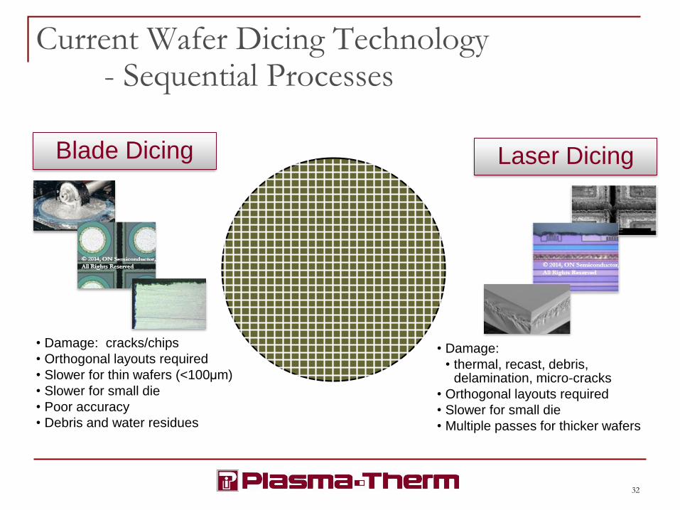
Current Wafer Dicing Technology - Sequential Processes
• Damage: cracks/chips
• Orthogonal layouts required
• Slower for thin wafers (<100μm)
• Slower for small die
• Poor accuracy
• Debris and water residues
Blade Dicing
• Damage:
• thermal, recast, debris, delamination, micro-cracks
• Orthogonal layouts required
• Slower for small die
• Multiple passes for thicker wafers
Laser Dicing
32
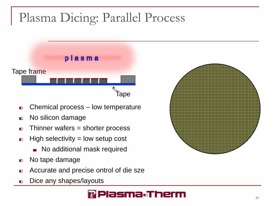
Plasma Dicing: Parallel Process
Chemical process – low temperature
No silicon damage
Thinner wafers = shorter process
High selectivity = low setup cost
No additional mask required
No tape damage
Accurate and precise ontrol of die sze
Dice any shapes/layouts
Tape frame
Tape
33
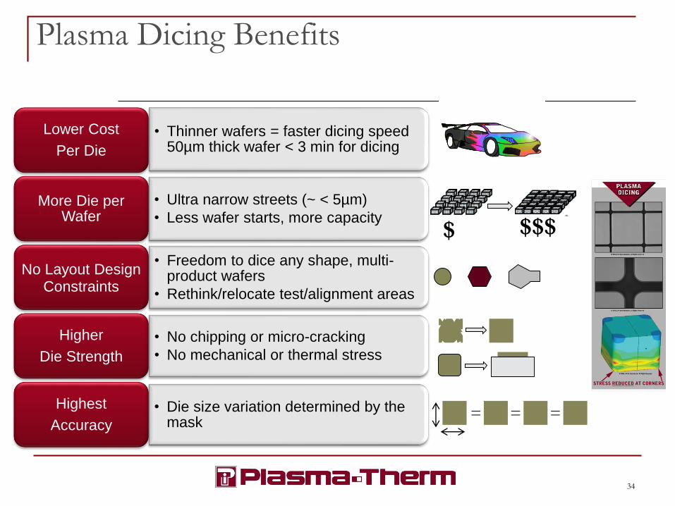
Plasma Dicing Benefits
• Thinner wafers = faster dicing speed 50µm thick wafer < 3 min for dicing
Lower Cost
Per Die
• Ultra narrow streets (~ < 5µm)
• Less wafer starts, more capacityMore Die per
Wafer
• Freedom to dice any shape, multi-product wafers
• Rethink/relocate test/alignment areas
No Layout Design Constraints
• No chipping or micro-cracking
• No mechanical or thermal stress
Higher
Die Strength
• Die size variation determined by the mask
Highest
Accuracy
$ $$$
= =
34
=
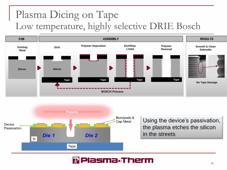
Plasma Dicing on TapeLow temperature, highly selective DRIE Bosch
35
EtchPolymer Deposition Etch/Dep.
LoopsPolymer
Removal
BOSCH Process
ASSEMBLY
Silicon
Existing
Mask
FAB
Smooth & Clean
Sidewalls
RESULTS
No Tape Damage
Silicon
Tape Tape Tape Tape
Using the device’s passivation,
the plasma etches the silicon
in the streets
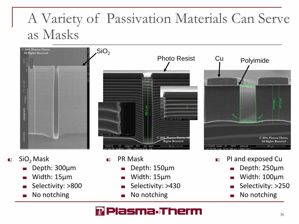
A Variety of Passivation Materials Can Serve as Masks
SiO2 MaskDepth: 300µmWidth: 15µmSelectivity: >800No notching
SiO2
Photo Resist PolyimideCu
PR MaskDepth: 150µmWidth: 15µmSelectivity: >430No notching
PI and exposed CuDepth: 250µmWidth: 100µmSelectivity: >250No notching
© 2014, Plasma-Therm,
All Rights Reserved
© 2014, Plasma-Therm, All
Rights Reserved
© 2014, Plasma-Therm,
All Rights Reserved
36
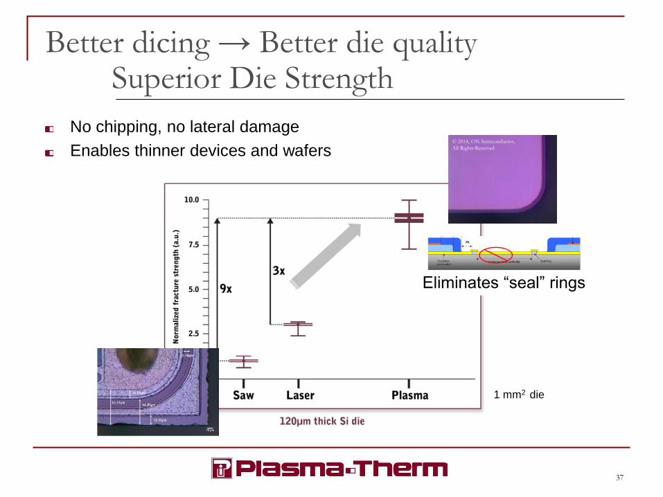
Better dicing → Better die qualitySuperior Die Strength
No chipping, no lateral damage
Enables thinner devices and wafers
1 mm2 die
© 2014, ON Semiconductor,
All Rights Reserved
© 2014, ON Semiconductor,
All Rights Reserved
~90µm
Eliminates “seal” rings
37
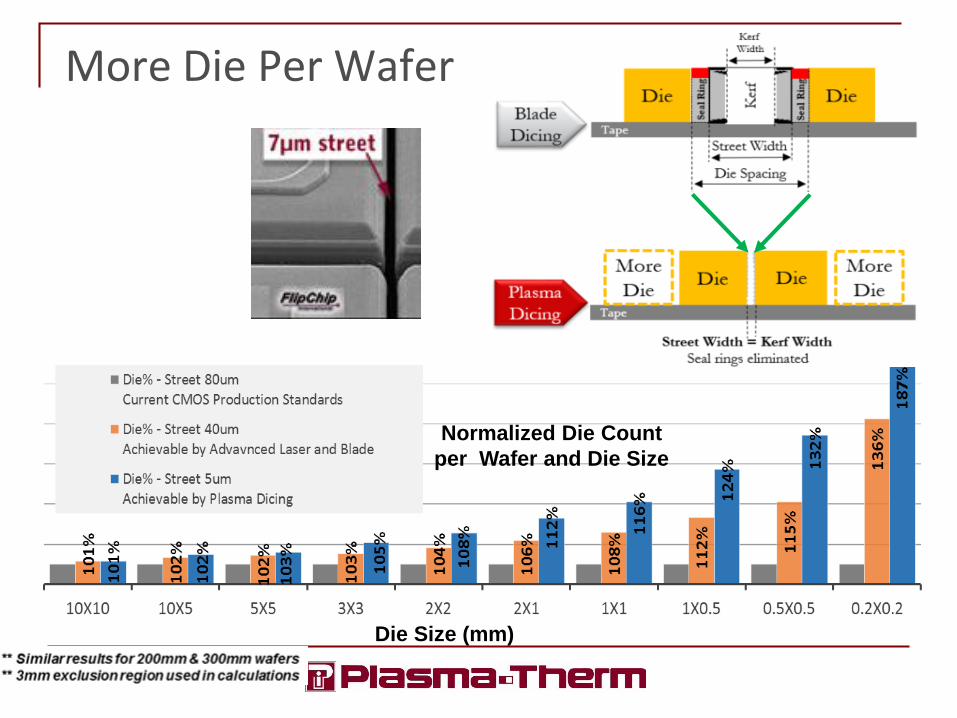
More Die Per Wafer
Normalized Die Count
per Wafer and Die Size
Die Size (mm)
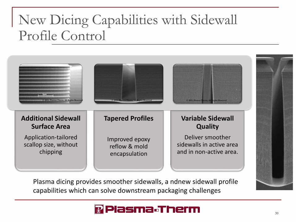
New Dicing Capabilities with Sidewall Profile Control
Additional Sidewall Surface Area
Application-tailored scallop size, without
chipping
Tapered Profiles
Improved epoxy reflow & mold encapsulation
Variable Sidewall Quality
Deliver smoother sidewalls in active area and in non-active area.
Plasma dicing provides smoother sidewalls, a ndnew sidewall profile capabilities which can solve downstream packaging challenges
© 2015, Plasma-Therm, All Rights Reserved
5μm
© 2015, Plasma-Therm, All Rights Reserved © 2015, Plasma-Therm, All Rights Reserved
39
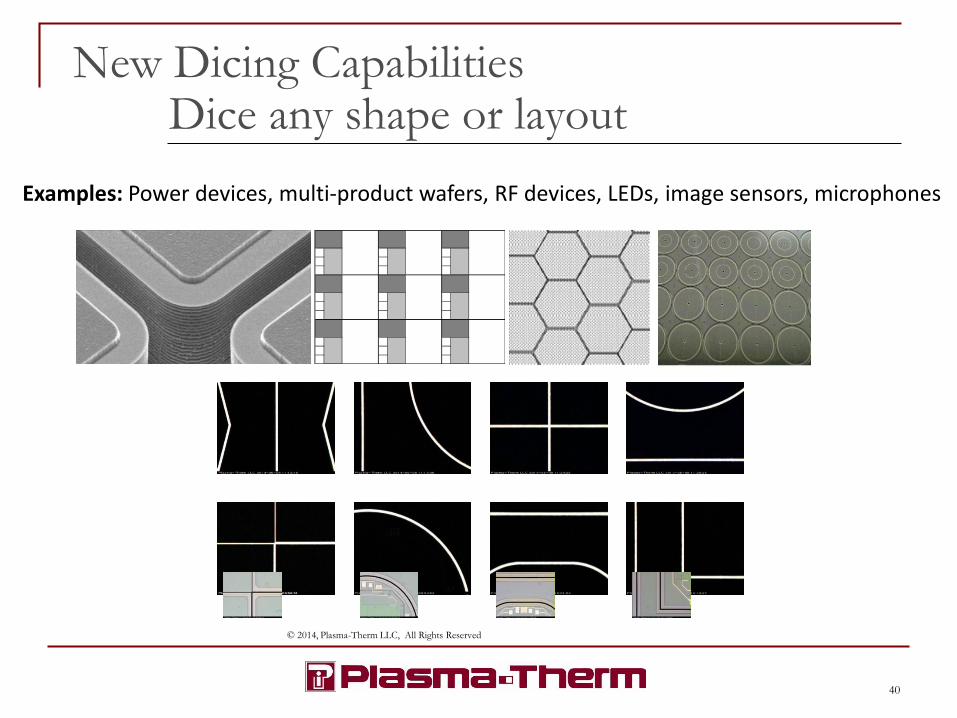
New Dicing CapabilitiesDice any shape or layout
© 2014, Plasma-Therm LLC, All Rights Reserved
Examples: Power devices, multi-product wafers, RF devices, LEDs, image sensors, microphones
40
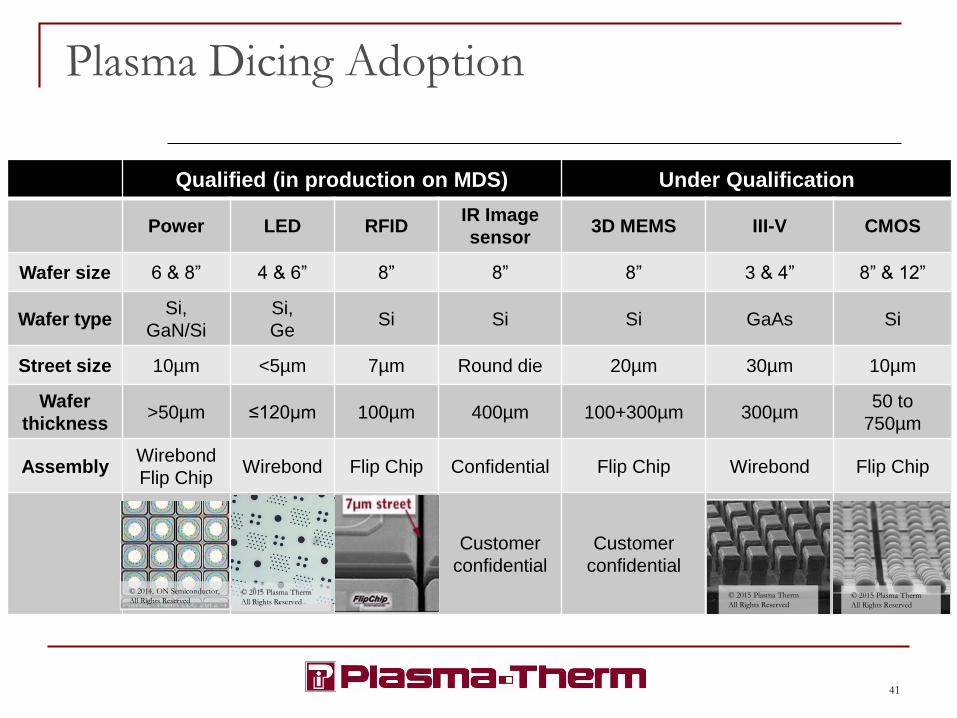
Plasma Dicing Adoption
Qualified (in production on MDS) Under Qualification
Power LED RFIDIR Image
sensor3D MEMS III-V CMOS
Wafer size 6 & 8” 4 & 6” 8” 8” 8” 3 & 4” 8” & 12”
Wafer typeSi,
GaN/Si
Si,
GeSi Si Si GaAs Si
Street size 10µm <5µm 7µm Round die 20µm 30µm 10µm
Wafer
thickness>50µm ≤120µm 100µm 400µm 100+300µm 300µm
50 to
750µm
AssemblyWirebond
Flip ChipWirebond Flip Chip Confidential Flip Chip Wirebond Flip Chip
Customer
confidential
Customer
confidential© 2014, ON Semiconductor,
All Rights Reserved© 2015 Plasma Therm
All Rights Reserved© 2015 Plasma Therm
All Rights Reserved
© 2015 Plasma Therm
All Rights Reserved
41
Acknowledgements
42
Christopher Johnston, Plasma Therm
Thierry Lazerand, Plasma Therm
Dr. Marco Notarianni, Plasma Therm
Dr. Kenneth Mackenzie, Plasma Therm
Yannick Pilloux, Plasma Therm
Julien Vitielo, Plasma Therm
Gordy Grivna, ON Semiconductor
Jason Doub, ON Semiconductor
Dr. Tomotak Tabushi, DISCO
Dr. Frank Wei, DISCO
Hideyuki Sando, DISCO
JS Jung, DISCO
Thank your for your contributions and materials to
prepare this presentation