l.royer– calice meeting @ desy – july 2010 laurent royer, samuel manen, pascal gay lpc...
TRANSCRIPT
L.Royer– Calice meeting @ DESY – July 2010
Laurent ROYER, Samuel MANEN, Pascal GAY
LPC Clermont-Ferrand
R&D activity @ LPC Clermont-Fddedicated to the VFE of the Si-W Ecal
L.Royer– Calice meeting @ DESY – July 2010
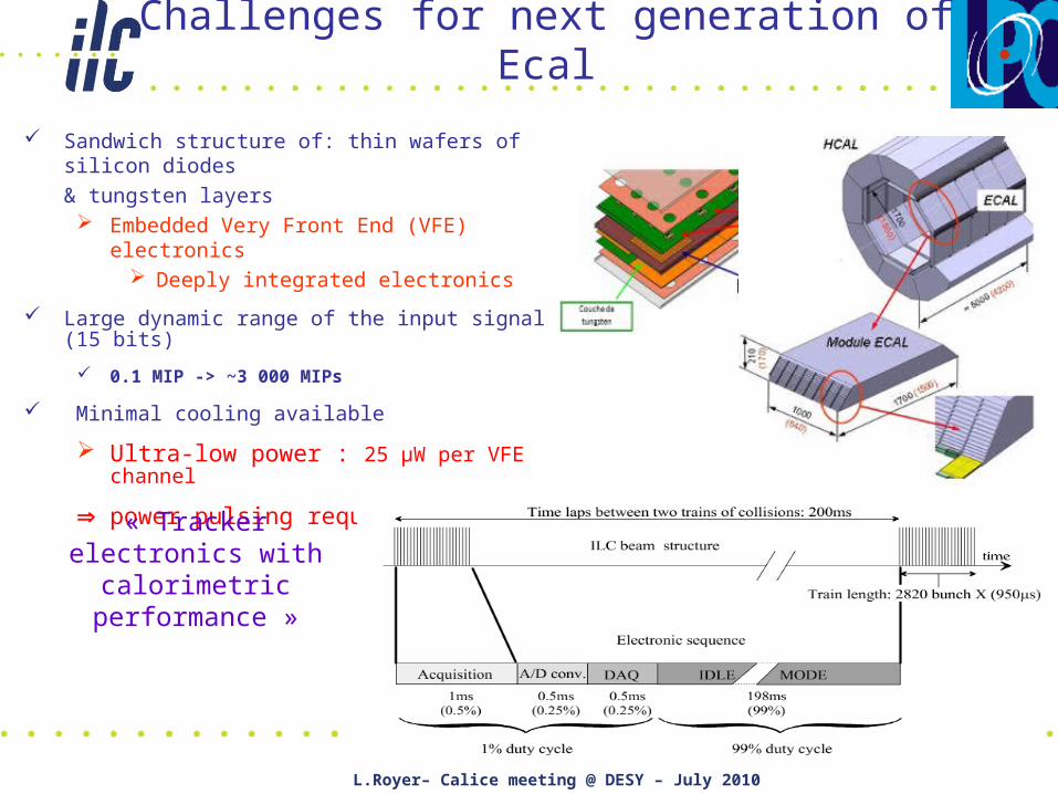
Challenges for next generation of Ecal
Sandwich structure of: thin wafers of silicon diodes
& tungsten layers Embedded Very Front End (VFE) electronics
Deeply integrated electronics
Large dynamic range of the input signal (15 bits)
0.1 MIP -> ~3 000 MIPs
Minimal cooling available
Ultra-low power : 25 µW per VFE channel
power pulsing required
« Tracker electronics withcalorimetric performance »

L.Royer– Calice meeting @ DESY – July 2010
Road map of the R&D activity @ LPC Clt-Fd
2002
2007
2008
2009
2-gain shaper w/ gated integrator analog memory
Low power ADC: 12-bit cyclic
preamp
shaper 10
analog memory
analog memory
shaper 1
12-bit ADC
Single VFE channel including ADC1.5 mW
6.5 mW
"Long is the road …"
Wilkinson ADC implemented in SKIROC chip
Low power ADC: 10-bit pipeline
L.Royer– Calice meeting @ DESY – July 2010
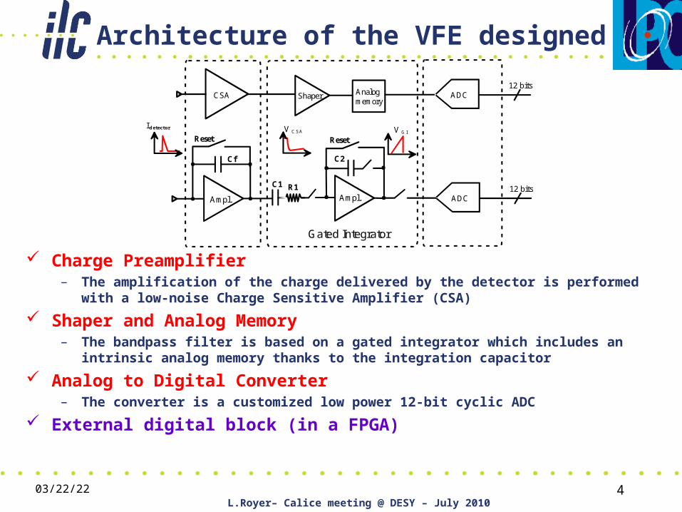
Architecture of the VFE designed
Charge Preamplifier– The amplification of the charge delivered by the detector is performed with a low-noise
Charge Sensitive Amplifier (CSA)
Shaper and Analog Memory– The bandpass filter is based on a gated integrator which includes an intrinsic analog
memory thanks to the integration capacitor
Analog to Digital Converter– The converter is a customized low power 12-bit cyclic ADC
External digital block (in a FPGA)
04/19/23 4
ShaperCSA Analogmemory
ADC12 bits
Ampl.
Cf
C1
C2
R1
Gated Integrator
Id e te c t o r V C S A
Reset
ADC12 bits
V G I
Ampl.
Reset
L.Royer– Calice meeting @ DESY – July 2010
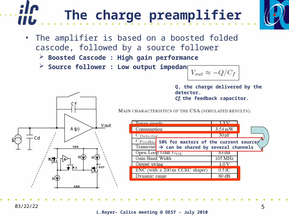
The charge preamplifier
04/19/23 5
• The amplifier is based on a boosted folded cascode, followed by a source follower Boosted Cascode : High gain performance Source follower : Low output impedance
Q, the charge delivered by the detector.Cf, the feedback capacitor.
50% for masters of the current sources can be shared by several channels
Cf
Cdi
A(p)Vout
M2
IN
OUT
I3-AI2
I1
GND
VDD
M1
M3
L.Royer– Calice meeting @ DESY – July 2010
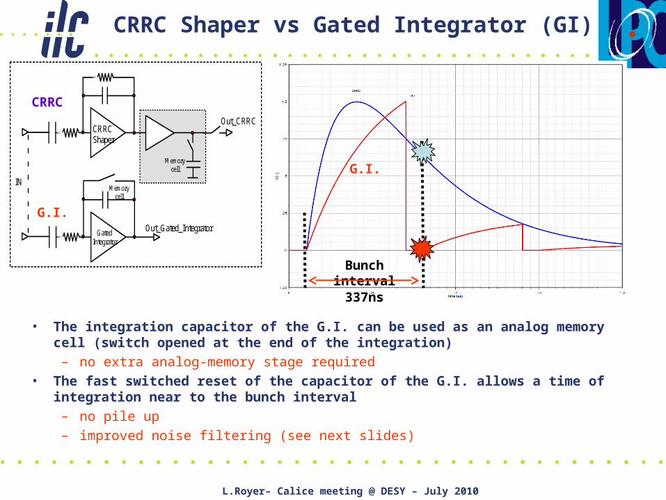
CRRC Shaper vs Gated Integrator (GI)
Bunch interval
CRRCShaper
Gated Integrator
IN
Out_CRRC
Out_Gated_Integrator
Memorycell
Memorycell
337ns
CRRC
G.I.
G.I.
• The integration capacitor of the G.I. can be used as an analog memory cell (switch opened at the end of the integration)
– no extra analog-memory stage required• The fast switched reset of the capacitor of the G.I. allows a time of integration near to
the bunch interval– no pile up– improved noise filtering (see next slides)
L.Royer– Calice meeting @ DESY – July 2010
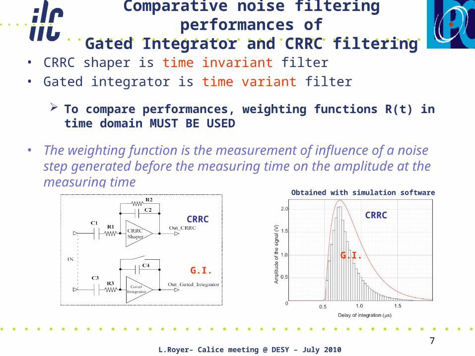
Comparative noise filtering performances ofGated Integrator and CRRC filtering
7
• CRRC shaper is time invariant filter• Gated integrator is time variant filter
To compare performances, weighting functions R(t) in time domain MUST BE USED
• The weighting function is the measurement of influence of a noise step generated before the measuring time on the amplitude at the measuring time
CRRC
G.I.
CRRC
G.I.
Obtained with simulation software
L.Royer– Calice meeting @ DESY – July 2010
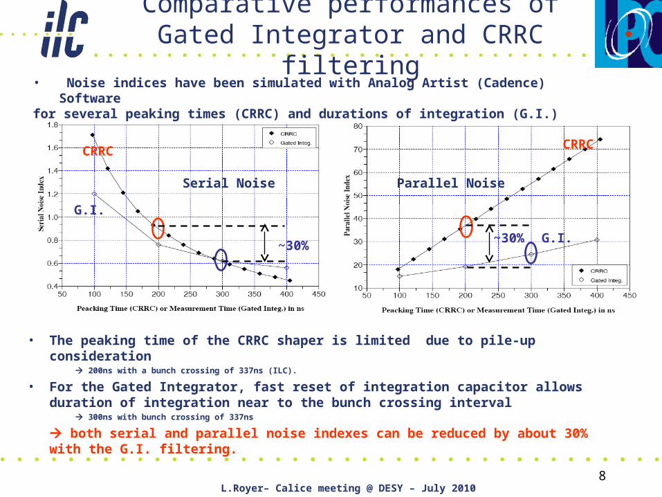
Comparative performances ofGated Integrator and CRRC filtering
• The peaking time of the CRRC shaper is limited due to pile-up consideration 200ns with a bunch crossing of 337ns (ILC).
• For the Gated Integrator, fast reset of integration capacitor allows duration of integration near to the bunch crossing interval
300ns with bunch crossing of 337ns
both serial and parallel noise indexes can be reduced by about 30% with the G.I. filtering.
8
Serial Noise Parallel Noise
CRRC
G.I.
G.I.
CRRC
~30%~30%
• Noise indices have been simulated with Analog Artist (Cadence) Software for several peaking times (CRRC) and durations of integration (G.I.)
L.Royer– Calice meeting @ DESY – July 2010
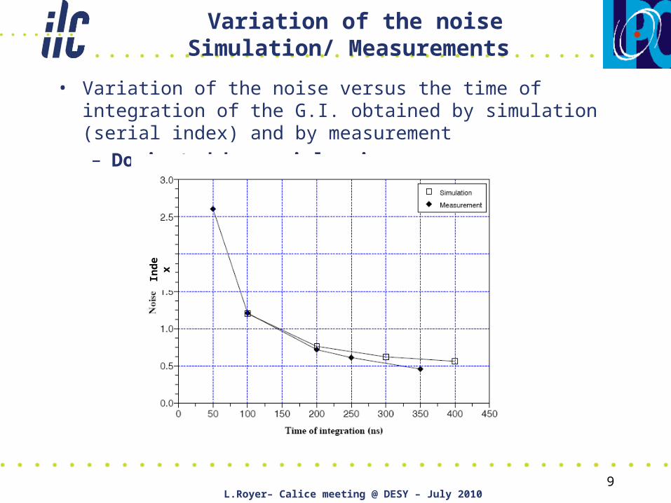
Variation of the noiseSimulation/ Measurements
• Variation of the noise versus the time of integration of the G.I. obtained by simulation (serial index) and by measurement– Dominated by serial noise.
9
Ind
ex
L.Royer– Calice meeting @ DESY – July 2010
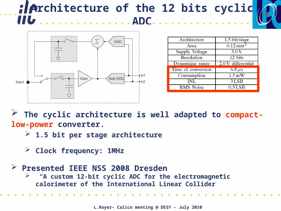
Architecture of the 12 bits cyclic ADC
The cyclic architecture is well adapted to compact-low-power converter.
1.5 bit per stage architecture
Clock frequency: 1MHz
Presented IEEE NSS 2008 Dresden “A custom 12-bit cyclic ADC for the electromagnetic calorimeter of the
International Linear Collider”
L.Royer– Calice meeting @ DESY – July 2010
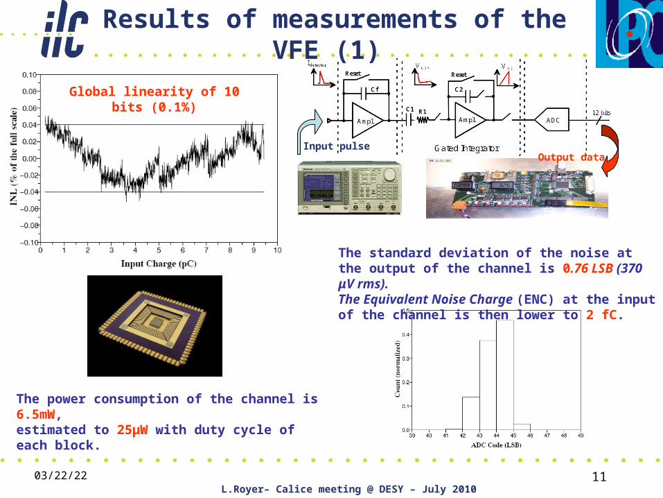
Results of measurements of the VFE (1)
04/19/23 11
Global linearity of 10 bits (0.1%)
The standard deviation of the noise at the output of the channel is 0.76 LSB (370 μV rms). The Equivalent Noise Charge (ENC) at the input of the channel is then lower to 2 fC.
The power consumption of the channel is 6.5mW,estimated to 25µW with duty cycle of each block.
Input pulseOutput data
L.Royer– Calice meeting @ DESY – July 2010
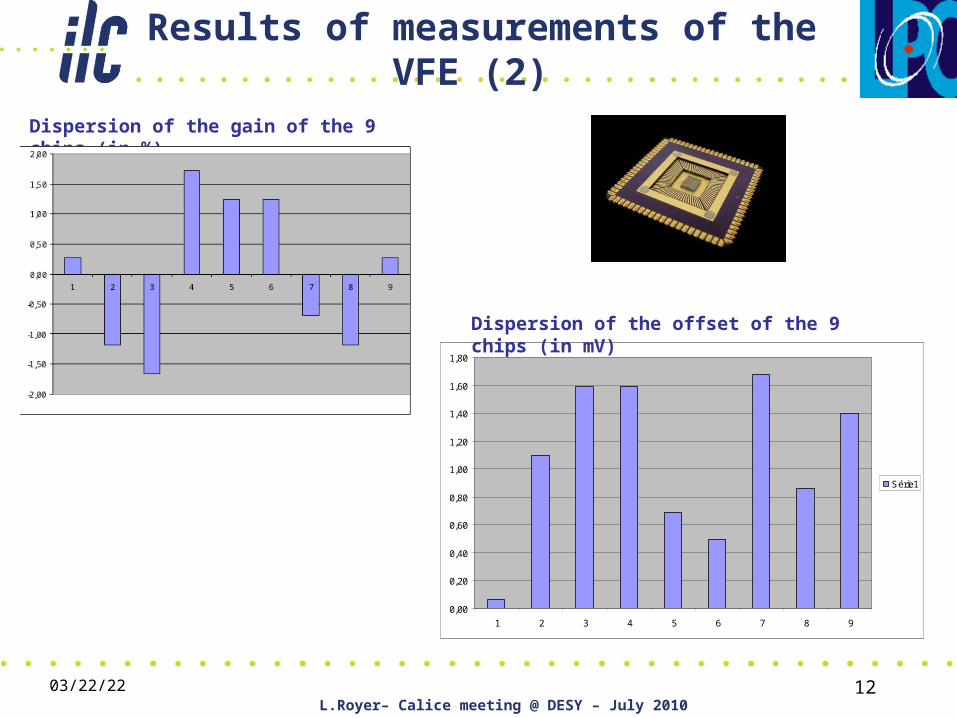
Results of measurements of the VFE (2)
04/19/23 12
Dispersion of the gain of the 9 chips (in %)
0,00
0,20
0,40
0,60
0,80
1,00
1,20
1,40
1,60
1,80
1 2 3 4 5 6 7 8 9
Série1
Dispersion of the offset of the 9 chips (in mV)
L.Royer– Calice meeting @ DESY – July 2010
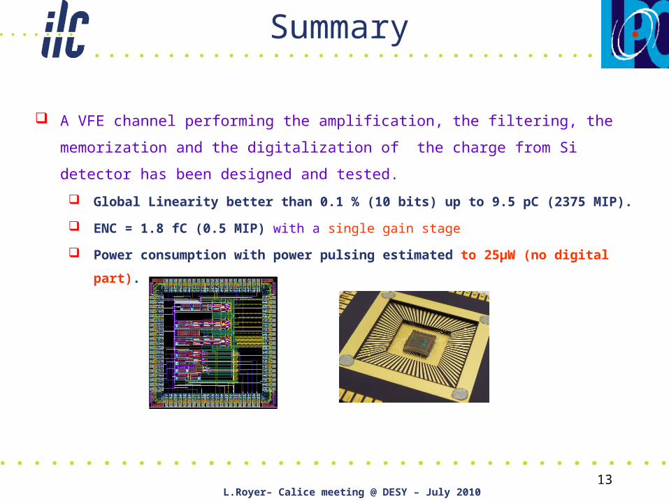
Summary
A VFE channel performing the amplification, the filtering, the memorization and the
digitalization of the charge from Si detector has been designed and tested.
Global Linearity better than 0.1 % (10 bits) up to 9.5 pC (2375 MIP).
ENC = 1.8 fC (0.5 MIP) with a single gain stage
Power consumption with power pulsing estimated to 25µW (no digital part).
13
L.Royer– Calice meeting @ DESY – July 2010
Perspectives Next steps
Improvement of the dynamic range up to 15 bits
Reduction of the output noise of the amplifier of the Gated Integrator
Integration of a multi-gain system on the CSA
Use of a multi gain shaping
Integration of the digital block, of the bandgap (ADC references), of the power pulsing, …
Test-bench for the VFE channel
realistic environment : wafer/ASU + VFE + (DIF)/DAQ
versatile and upgradable
connected to wafer test-bench already in LPC-Clfd
have to be discussed with LPC-Clfd management for Manpower resource
Synergy with the Collaboration has to be defined
14
L.Royer– Calice meeting @ DESY – July 2010
spare
L.Royer– Calice meeting @ DESY – July 2010
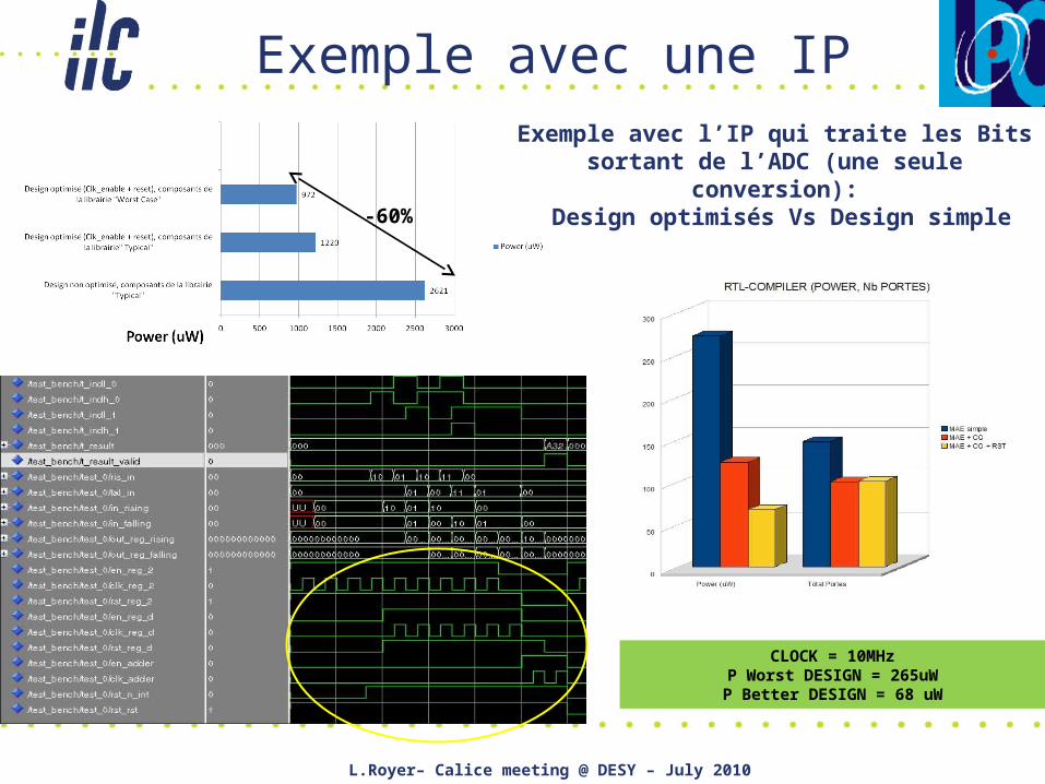
Exemple avec une IPExemple avec l’IP qui traite les Bits sortant de
l’ADC (une seule conversion): Design optimisés Vs Design simple
CLOCK = 10MHzP Worst DESIGN = 265uWP Better DESIGN = 68 uW
-60%
L.Royer– Calice meeting @ DESY – July 2010
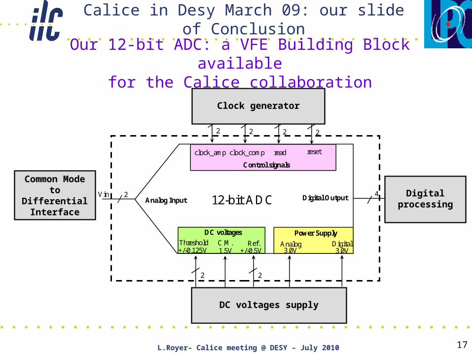
2Vin 4Analog Input Digital Output
Power Supply
Analog Digital3.0V3.0V
DC voltages
Threshold Ref.+/-0.125V +/-0.5V
C.M.1.5V
Control signals
clock_amp clock_comp read reset
2 2
2 2 2 2
12-bit ADC
Clock generator
DC voltages supply
Digital processing
Common Mode to
Differential Interface
17
Calice in Desy March 09: our slide of Conclusion
Our 12-bit ADC: a VFE Building Block availablefor the Calice collaboration