shi induced silicide formation and surface morphology at co/si system
TRANSCRIPT
www.elsevier.com/locate/apsusc
Applied Surface Science 253 (2006) 1165–1169
SHI induced silicide formation and surface morphology
at Co/Si system
Garima Agarwal, Pratibha Sharma, I.P. Jain *
Material Science Laboratory, Centre for Non-Conventional Energy Resources, 14-Vigyan Bhawan,
University of Rajasthan, Jaipur 302004, India
Received 6 October 2005; received in revised form 25 January 2006; accepted 25 January 2006
Available online 18 April 2006
Abstract
Ion beam mixing is a useful technique to produce modifications at the surface and interface of the solid material. In the present work, ion beam
induced modifications at Co/Si interface using 120 MeVAu-ion irradiation has been studied at ion fluences in the range of 1012 to 1014 ions/cm2 by
secondary ion mass spectroscopy (SIMS) technique and calculated mixing efficiency at the interface. Silicide formation has been discussed on the
basis of swift heavy ion (SHI) irradiation induced effects. Surface morphology and roughness of irradiated system with fluence 5 � 1013 and
1 � 1014 ions/cm2 is studied by scanning tunneling microscopy (STM). Roughness of the surface shows marks of melting process and confirms the
appearance of some pinholes in the reacted Co/Si system. Comparative study was also undertaken on annealed sample at 300 8C and then irradiated
at a dose 1 � 1014 ions/cm2.
# 2006 Elsevier B.V. All rights reserved.
Keywords: Ion beam mixing; Surface; Interface; Silicide; Ion irradiation
1. Introduction
Metal on silicon have been the subject of investigations over
the last five decades because of the importance of silicides for
contact in the field of microelectronics where silicides are the
compound formation at the metal/Si interface. The extensive
study of metal silicides is related to their applications in silicon
technology as low resistivity interconnect, chemical stability,
low fabrication temperature, small lattice mismatch with
silicon and a range of Schottky barrier heights. Techniques
involved in the formation of metal silicides are solid state
reaction, already existing technique and the ion beam mixing,
new emerging one. Ion beam induced metal silicides have
grater advantages over existing technique formation as it
provides a better smooth surface and it can control the
temperature during the formation as the rise in temperature is
not so good for silicon devices.
Ion beam mixing at the interface of different species using keV
is well understood subject [1]. For this energy regime, mixing at
* Corresponding author. Tel.: +91 141 2701602/9726; fax: +91 141 2701880.
E-mail address: [email protected] (I.P. Jain).
0169-4332/$ – see front matter # 2006 Elsevier B.V. All rights reserved.
doi:10.1016/j.apsusc.2006.01.059
the interface of either metal/metal or metal/semiconductor
system mainly caused by ballistic effects, called as nuclear-loss
induced ion beam mixing. At higher energies with MeV beams
ions loss energy predominantly to the electronic system of the
material called as electronic loss. In recent years, many effects
involving atomic displacement via electronic energy loss such as
annealing [2], amorphization [3] and ion beam mixing [4] have
attracted considerable interest both for understanding the
phenomena and for technological applications.
Ion beam mixing in thin metal film/semiconductor systems
has been widely used to form both equilibrium and metalstable
phases [5–7]. In addition to involving lower processing
temperature, this technique provides a high degree of spatial
selectivity. Metal/semiconductor system is a good choice to
study swift heavy ion (SHI), the ions having energy in MeV
range, induced mixing from the fundamental ion–solid
interaction point of view as well as their wide applications.
Hence, the reaction of metal on Si under ion irradiation leads
to the formation of metal silicides. Among the various silicides
most of present works have been concentrated on NiSi2, FeSi2,
TiSi2, CoSi2, etc.
We have planned the study of CoSi2 formation as it has been
receiving increasing importance for low resistance, high
G. Agarwal et al. / Applied Surface Science 253 (2006) 1165–11691166
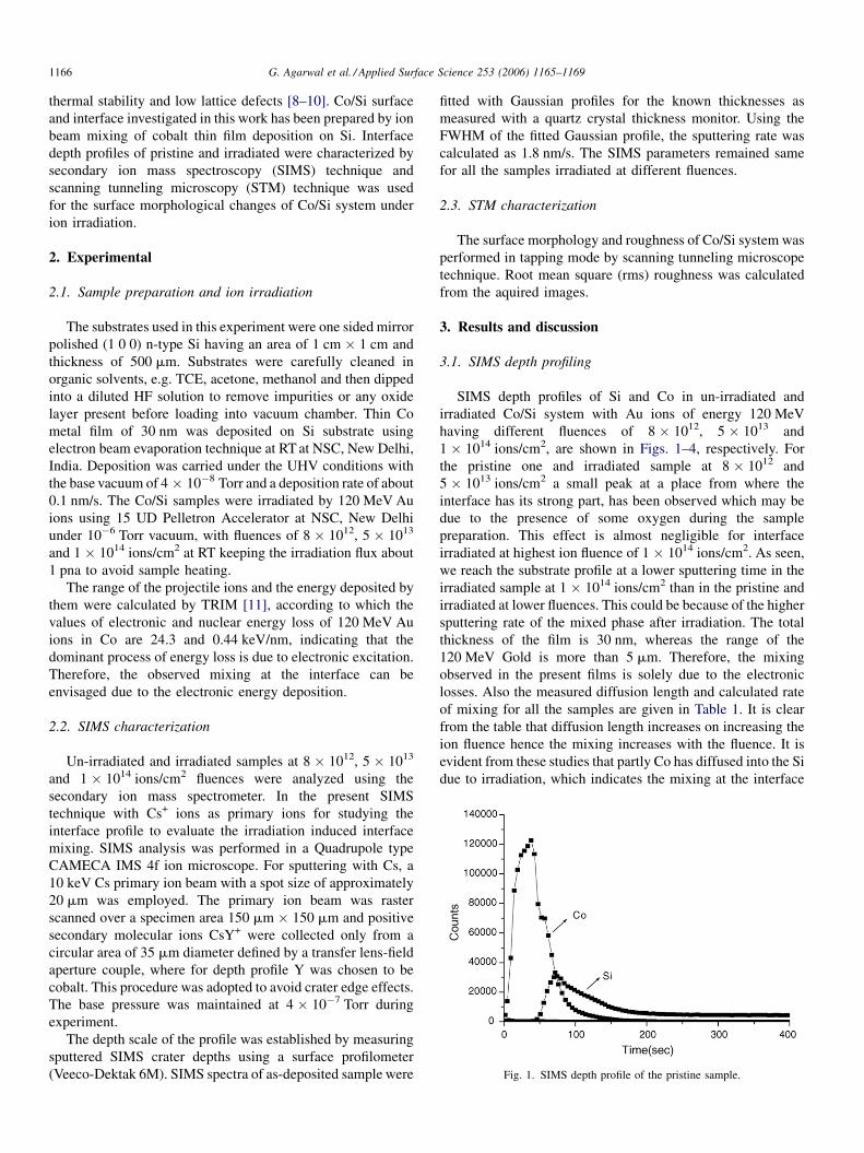
Fig. 1. SIMS depth profile of the pristine sample.
thermal stability and low lattice defects [8–10]. Co/Si surface
and interface investigated in this work has been prepared by ion
beam mixing of cobalt thin film deposition on Si. Interface
depth profiles of pristine and irradiated were characterized by
secondary ion mass spectroscopy (SIMS) technique and
scanning tunneling microscopy (STM) technique was used
for the surface morphological changes of Co/Si system under
ion irradiation.
2. Experimental
2.1. Sample preparation and ion irradiation
The substrates used in this experiment were one sided mirror
polished (1 0 0) n-type Si having an area of 1 cm � 1 cm and
thickness of 500 mm. Substrates were carefully cleaned in
organic solvents, e.g. TCE, acetone, methanol and then dipped
into a diluted HF solution to remove impurities or any oxide
layer present before loading into vacuum chamber. Thin Co
metal film of 30 nm was deposited on Si substrate using
electron beam evaporation technique at RT at NSC, New Delhi,
India. Deposition was carried under the UHV conditions with
the base vacuum of 4 � 10�8 Torr and a deposition rate of about
0.1 nm/s. The Co/Si samples were irradiated by 120 MeV Au
ions using 15 UD Pelletron Accelerator at NSC, New Delhi
under 10�6 Torr vacuum, with fluences of 8 � 1012, 5 � 1013
and 1 � 1014 ions/cm2 at RT keeping the irradiation flux about
1 pna to avoid sample heating.
The range of the projectile ions and the energy deposited by
them were calculated by TRIM [11], according to which the
values of electronic and nuclear energy loss of 120 MeV Au
ions in Co are 24.3 and 0.44 keV/nm, indicating that the
dominant process of energy loss is due to electronic excitation.
Therefore, the observed mixing at the interface can be
envisaged due to the electronic energy deposition.
2.2. SIMS characterization
Un-irradiated and irradiated samples at 8 � 1012, 5 � 1013
and 1 � 1014 ions/cm2 fluences were analyzed using the
secondary ion mass spectrometer. In the present SIMS
technique with Cs+ ions as primary ions for studying the
interface profile to evaluate the irradiation induced interface
mixing. SIMS analysis was performed in a Quadrupole type
CAMECA IMS 4f ion microscope. For sputtering with Cs, a
10 keV Cs primary ion beam with a spot size of approximately
20 mm was employed. The primary ion beam was raster
scanned over a specimen area 150 mm � 150 mm and positive
secondary molecular ions CsY+ were collected only from a
circular area of 35 mm diameter defined by a transfer lens-field
aperture couple, where for depth profile Y was chosen to be
cobalt. This procedure was adopted to avoid crater edge effects.
The base pressure was maintained at 4 � 10�7 Torr during
experiment.
The depth scale of the profile was established by measuring
sputtered SIMS crater depths using a surface profilometer
(Veeco-Dektak 6M). SIMS spectra of as-deposited sample were
fitted with Gaussian profiles for the known thicknesses as
measured with a quartz crystal thickness monitor. Using the
FWHM of the fitted Gaussian profile, the sputtering rate was
calculated as 1.8 nm/s. The SIMS parameters remained same
for all the samples irradiated at different fluences.
2.3. STM characterization
The surface morphology and roughness of Co/Si system was
performed in tapping mode by scanning tunneling microscope
technique. Root mean square (rms) roughness was calculated
from the aquired images.
3. Results and discussion
3.1. SIMS depth profiling
SIMS depth profiles of Si and Co in un-irradiated and
irradiated Co/Si system with Au ions of energy 120 MeV
having different fluences of 8 � 1012, 5 � 1013 and
1 � 1014 ions/cm2, are shown in Figs. 1–4, respectively. For
the pristine one and irradiated sample at 8 � 1012 and
5 � 1013 ions/cm2 a small peak at a place from where the
interface has its strong part, has been observed which may be
due to the presence of some oxygen during the sample
preparation. This effect is almost negligible for interface
irradiated at highest ion fluence of 1 � 1014 ions/cm2. As seen,
we reach the substrate profile at a lower sputtering time in the
irradiated sample at 1 � 1014 ions/cm2 than in the pristine and
irradiated at lower fluences. This could be because of the higher
sputtering rate of the mixed phase after irradiation. The total
thickness of the film is 30 nm, whereas the range of the
120 MeV Gold is more than 5 mm. Therefore, the mixing
observed in the present films is solely due to the electronic
losses. Also the measured diffusion length and calculated rate
of mixing for all the samples are given in Table 1. It is clear
from the table that diffusion length increases on increasing the
ion fluence hence the mixing increases with the fluence. It is
evident from these studies that partly Co has diffused into the Si
due to irradiation, which indicates the mixing at the interface

G. Agarwal et al. / Applied Surface Science 253 (2006) 1165–1169 1167
Fig. 2. SIMS depth profile of irradiated sample at 8 � 1012 ions/cm2.
Fig. 3. SIMS depth profile of irradiated sample at 5 � 1013 ions/cm2.
Fig. 4. SIMS depth profile of irradiated sample at 1 � 1014 ions/cm2.
leading to the formation of different phases of cobalt silicide,
e.g. Co2Si, CoSi and CoSi2. The possible mechanism of the
mixing at the interface of two different species can be explained
with the help of two models named Coulomb explosion and
Thermal spike which account for the atomic motion induce by
electronic excitation. But the formation of CoSi2 which is the
most stable phase in the series of cobalt silicides, can be
attributed due to the Thermal spike model as Co is a metal and
the Coulomb explosion can be ruled out since it works better for
insulator systems. Although the Thermal spike has already well
employed for metal/metal and insulator/insulator systems to
Table 1
Diffusion length, mixing rate and mixing efficiency with fluence
Fluence, F (ions/cm2) Diffusion length, X (nm) Mixin
Unirradiated 16.0 –
8 � 1012 20.0 5000.
5 � 1013 39.0 3042.
1 � 1014 52.7 2777.
show that interface mixing is due to inter-diffusion in the melt
phase. But in insulators the possibility of atomic motion by the
process of Coulomb explosion cannot be ignored. Therefore,
the present Co/Si mixing is better case to consider under
thermal spike effect. For such hypothesis, we plan an
approximate estimate of the diffusivity in the molten state.
To examine this estimation, we calculate the diffusion
coefficient [12,13] for Co as
D ¼ DX2
2tn
where tn is the diffusion time and DX2 is given as:
DX2 ¼ X2ðFÞ � X2ð0Þ
where X is the diffusion length.
On calculation the diffusivity D at the interface turns out to
be of the order of�10�6 m2 s�1, which is clearly in the range of
the inter-diffusion constants known from liquids and hence
supports the thermal spike hypothesis. Thus, the ion beam
induced by swift heavy ions in the present experiments can be
attributed as consequence of inter-diffusion in the melt phase
which is the novelty of these results to understand better the
mechanism behind the whole process.
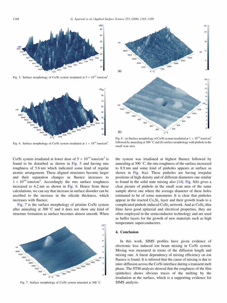
3.2. Surface morphology
The variation of surface roughness and morphology of Co/Si
system under irradiation of 5 � 1013 and 1 � 1014 ions/cm2
fluences has been investigated by STM. Surface morphology is
greatly influenced by the irradiation fluence as the surface of
g rate, k = DX2/F (nm4/ion) Mixing efficiency, k/Se (nm5/keV)
–
00 205.76
00 125.18
29 114.29
G. Agarwal et al. / Applied Surface Science 253 (2006) 1165–11691168
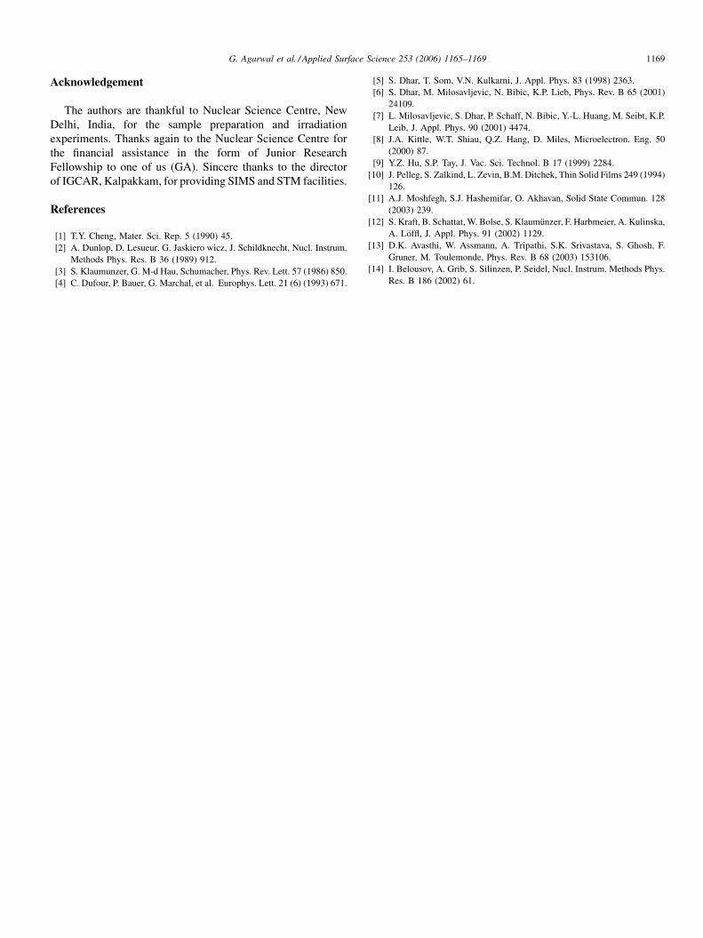
Fig. 6. Surface morphology of Co/Si system irradiated at 1 � 1014 ions/cm2.
Fig. 8. (a) Surface morphology of Co/Si system irradiated at 1 � 1014 ions/cm2
followed by annealing at 300 8C and (b) surface morphology with pinhole in the
small scan area.
Fig. 5. Surface morphology of Co/Si system irradiated at 5 � 1013 ions/cm2.
Co/Si system irradiated at lower dose of 5 � 1013 ions/cm2 is
found to be disturbed as shown in Fig. 5 and having rms
roughness of 5.6 nm which indicated some kind of regular
atomic arrangement. These aligned structures become larger
and their separation changes as fluence increases to
1 � 1014 ions/cm2. Accordingly the rms surface roughness
increased to 6.2 nm as shown in Fig. 6. Hence from these
calculations, we can say that increase in surface disorder can be
ascribed to the increase in the silicide thickness, which
increases with fluence.
Fig. 7 is the surface morphology of pristine Co/Si system
after annealing at 300 8C and it does not show any kind of
structure formation as surface becomes almost smooth. When
Fig. 7. Surface morphology of Co/Si system annealed at 300 8C.
the system was irradiated at highest fluence followed by
annealing at 300 8C, the rms roughness of the surface increased
to 8.9 nm and some kind of pinholes appears at surface as
shown in Fig. 8(a). These pinholes are having irregular
positions of high density and of different diameters one similar
to found in the solid state mixing also [14]. Fig. 8(b) gives a
clear picture of pinhole in the small scan area of the same
sample above one where the average diameter of these holes
estimated to be of some nanometer. It is clear that pinholes
appear in the reacted CoxSiy layer and their growth leads to a
complicated pinhole induced CoSi2 network. And as CoSi2 thin
films have good epitaxial and electrical properties, they are
often employed in the semiconductor technology and are used
as buffer layers for the growth of new materials such as high
temperature superconductors.
4. Conclusion
In this work, SIMS profiles have given evidence of
electronic loss induced ion beam mixing in Co/Si system.
Mixing was measured in terms of the diffusion length and
mixing rate. A linear dependency of mixing efficiency on ion
fluence is found. It is inferred that the cause of mixing is due to
inter-diffusion across the Co/Si interface during a transient melt
phase. The STM analysis showed that the roughness of the film
(pinholes) shows obvious traces of the melting by the
irradiation at the surface, which is a supporting evidence for
SIMS analysis.
G. Agarwal et al. / Applied Surface Science 253 (2006) 1165–1169 1169
Acknowledgement
The authors are thankful to Nuclear Science Centre, New
Delhi, India, for the sample preparation and irradiation
experiments. Thanks again to the Nuclear Science Centre for
the financial assistance in the form of Junior Research
Fellowship to one of us (GA). Sincere thanks to the director
of IGCAR, Kalpakkam, for providing SIMS and STM facilities.
References
[1] T.Y. Cheng, Mater. Sci. Rep. 5 (1990) 45.
[2] A. Dunlop, D. Lesueur, G. Jaskiero wicz, J. Schildknecht, Nucl. Instrum.
Methods Phys. Res. B 36 (1989) 912.
[3] S. Klaumunzer, G. M-d Hau, Schumacher, Phys. Rev. Lett. 57 (1986) 850.
[4] C. Dufour, P. Bauer, G. Marchal, et al. Europhys. Lett. 21 (6) (1993) 671.
[5] S. Dhar, T. Som, V.N. Kulkarni, J. Appl. Phys. 83 (1998) 2363.
[6] S. Dhar, M. Milosavljevic, N. Bibic, K.P. Lieb, Phys. Rev. B 65 (2001)
24109.
[7] L. Milosavljevic, S. Dhar, P. Schaff, N. Bibic, Y.-L. Huang, M. Seibt, K.P.
Leib, J. Appl. Phys. 90 (2001) 4474.
[8] J.A. Kittle, W.T. Shiau, Q.Z. Hang, D. Miles, Microelectron. Eng. 50
(2000) 87.
[9] Y.Z. Hu, S.P. Tay, J. Vac. Sci. Technol. B 17 (1999) 2284.
[10] J. Pelleg, S. Zalkind, L. Zevin, B.M. Ditchek, Thin Solid Films 249 (1994)
126.
[11] A.J. Moshfegh, S.J. Hashemifar, O. Akhavan, Solid State Commun. 128
(2003) 239.
[12] S. Kraft, B. Schattat, W. Bolse, S. Klaumunzer, F. Harbmeier, A. Kulinska,
A. Loffl, J. Appl. Phys. 91 (2002) 1129.
[13] D.K. Avasthi, W. Assmann, A. Tripathi, S.K. Srivastava, S. Ghosh, F.
Gruner, M. Toulemonde, Phys. Rev. B 68 (2003) 153106.
[14] I. Belousov, A. Grib, S. Silinzen, P. Seidel, Nucl. Instrum. Methods Phys.
Res. B 186 (2002) 61.