two-step beam-forming using space-frequency trans ... · two-step beam-forming using...
TRANSCRIPT
Two-step beam-forming using space-frequency trans-formation in a time-multiplexed phased array receiverCitation for published version (APA):Deng, W. (2011). Two-step beam-forming using space-frequency trans-formation in a time-multiplexed phasedarray receiver. Eindhoven: Technische Universiteit Eindhoven. https://doi.org/10.6100/IR723153
DOI:10.6100/IR723153
Document status and date:Published: 01/01/2011
Document Version:Publisher’s PDF, also known as Version of Record (includes final page, issue and volume numbers)
Please check the document version of this publication:
• A submitted manuscript is the version of the article upon submission and before peer-review. There can beimportant differences between the submitted version and the official published version of record. Peopleinterested in the research are advised to contact the author for the final version of the publication, or visit theDOI to the publisher's website.• The final author version and the galley proof are versions of the publication after peer review.• The final published version features the final layout of the paper including the volume, issue and pagenumbers.Link to publication
General rightsCopyright and moral rights for the publications made accessible in the public portal are retained by the authors and/or other copyright ownersand it is a condition of accessing publications that users recognise and abide by the legal requirements associated with these rights.
• Users may download and print one copy of any publication from the public portal for the purpose of private study or research. • You may not further distribute the material or use it for any profit-making activity or commercial gain • You may freely distribute the URL identifying the publication in the public portal.
If the publication is distributed under the terms of Article 25fa of the Dutch Copyright Act, indicated by the “Taverne” license above, pleasefollow below link for the End User Agreement:www.tue.nl/taverne
Take down policyIf you believe that this document breaches copyright please contact us at:[email protected] details and we will investigate your claim.
Download date: 03. Jul. 2020

Two-Step Beam-Forming Using Space-Frequency Transformation in a Time-Multiplexed Phased-Array
Receiver
Wei Deng

Front cover: Chip photo of the system presented in Chapter 8
Back cover: Wei Deng photo and short Curriculum Vitae

Two-Step Beam-Forming Using Space-Frequency Transformation in a Time-Multiplexed Phased-Array
Receiver
PROEFSCHRIFT
ter verkrijging van de graad van doctor aan de Technische Universiteit Eindhoven, op gezag van de rector magnificus, prof.dr.ir. C.J. van Duijn, voor een commissie aangewezen door het College voor Promoties in het openbaar te verdedigen
op maandag 28 november 2011 om 14.00 uur
door
Wei Deng
geboren te Wuhan, China

Dit proefschrift is goedgekeurd door de promotor:
prof.dr.ir. A.H.M. van Roermund
Copromotor: dr.ir. R. Mahmoudi
A catalogue record is available from the Eindhoven University of Technology Library.
CIP-DATA LIBRARY TECHNISCHE UNIVERSITEIT EINDHOVEN
Wei Deng
Two-Step Beam-Forming Using Space-Frequency Transformation in a Time-Multiplexed Phased-Array Receiver / by Wei Deng. – Eindhoven : Technische Universiteit Eindhoven, 2011. Proefschrift. – ISBN: NUR 959 Key words: 30GHz / SiGe mm wave integrated circuit design / phased array / receiver / beam forming / multiplexing / switching
Copyright © 2011 by Wei Deng, Eindhoven
All rights reserved. No part of this publication may be reproduced or transmitted in any form or by any means, electronic, mechanical, including photocopy, recording, or any information sto-rage and retrieval system without the prior written permission of the copyright owner.

To my parents, and to my wife, Yan Huang.

Samenstelling van de promotiecommissie:
prof. dr. ir. A.C.P.M. Backx, Technische Universiteit Eindhoven, voorzitter prof. dr. ir. A.H.M. van Roermund, Technische Universiteit Eindhoven, promotor dr. ir. R. Mahmoudi, Technische Universiteit Eindhoven, co-promotor prof. dr. ir. D.M.W. Leenaerts, Technische Universiteit Eindhoven prof. dr. ir. F.E. Vliet, University of Twente prof. ir. A. van Ardenne, Chalmers University of Technology prof. dr. ir. A.B. Smolders, Technische Universiteit Eindhoven dr. ir. G.H.C. van Werkhoven, Thales Nederland
.

vii
Contents
Contents ............................................................................ vii
Glossary .............................................................................. xi
1 Introduction .................................................................. 1
1.1 Motivation ....................................................................................................................... 1
1.2 Background...................................................................................................................... 3
1.3 Problem statement and research strategy .................................................................... 4
1.4 Thesis outline .................................................................................................................. 5
2 Basic concepts ............................................................... 7
2.1 Receiver system basics ................................................................................................... 7
2.1.1 Noise .................................................................................................................... 8
2.1.2 Non-linearity ..................................................................................................... 10
2.1.3 Dynamic Range ................................................................................................ 13
2.2 Phase modulation basics .............................................................................................. 14
2.3 Phased-array basics ....................................................................................................... 18
3 Single and multipath receiver: a system approach ..........25
3.1 Translating ADC parameters to RF domain ............................................................ 26
3.1.1 ADC model ....................................................................................................... 27

viii Contents
3.1.2 ADC noise ........................................................................................................ 27
3.1.3 ADC non-linearity ........................................................................................... 29
3.2 Mapping ADC parameters to system design ............................................................ 32
3.3 Receiver system optimization method ...................................................................... 35
3.3.1 Receiver signal flow diagram .......................................................................... 35
3.3.2 Optimization method ...................................................................................... 38
3.4 Analog beam-forming .................................................................................................. 39
3.5 Digital beam-forming ................................................................................................... 45
3.6 General case of beam-forming ................................................................................... 50
3.7 Conclusion ..................................................................................................................... 52
4 Two-step beam-forming: multiplexing architecture ........53
4.1 Multiplexing architecture introduction ...................................................................... 53
4.2 Spatial to frequency mapping ..................................................................................... 57
4.3 Two steps of spatial filtering ....................................................................................... 57
4.4 Phased-array analog and digital co-design ................................................................ 58
4.5 Generalized phased-array system design ................................................................... 58
5 Multiplexing architecture, ideal behavior ....................... 61
5.1 Analog multiplexing ..................................................................................................... 62
5.1.1 Properties of the switching signal .................................................................. 62
5.1.2 Pulse modulation .............................................................................................. 64
5.1.3 Combination in the analog domain ............................................................... 68
5.2 Spatial to frequency mapping ..................................................................................... 70
5.2.1 Space to frequency mapping coefficient Dn ................................................. 70
5.2.2 Translation from voltage to power domain, Dn to Pxn ................................ 76
5.2.3 Coarse beam pattern RxN by frequency selectivity ..................................... 79
5.3 Digital de-multiplexing and phase-shifting ............................................................... 82
5.4 Array pattern ................................................................................................................. 86
5.5 Conclusion ..................................................................................................................... 89

Contents ix
6 Multiplexing architecture, non-ideal behavior ................ 91
6.1 Angle deviation ............................................................................................................. 92
6.2 Non-ideal switches ....................................................................................................... 93
6.3 Noise in a multiplexing system ................................................................................... 96
6.4 Frequency mixing ......................................................................................................... 99
6.5 System simulations ..................................................................................................... 100
6.6 Power flow diagram for a multiplexed architecture .............................................. 103
6.7 Conclusion ................................................................................................................... 105
7 Designs for the 30GHz components ............................. 107
7.1 Design requirements .................................................................................................. 107
7.2 LNA and Multiplexer ................................................................................................. 108
7.2.1 Circuit design .................................................................................................. 108
7.2.2 Measurements ................................................................................................. 111
7.3 LNA-multiplexer-mixer combination...................................................................... 114
7.3.1 Circuit design .................................................................................................. 114
7.3.2 Measurements ................................................................................................. 116
7.4 Clock generator ........................................................................................................... 117
7.4.1 Circuit design .................................................................................................. 117
7.4.2 Measurements ................................................................................................. 120
7.5 Input delay line............................................................................................................ 121
7.5.1 Circuit design .................................................................................................. 121
7.5.2 Measurements ................................................................................................. 126
7.6 Power amplifier ........................................................................................................... 127
7.6.1 Circuit design .................................................................................................. 127
7.6.2 Measurements ................................................................................................. 129
7.6.3 Trouble shooting ............................................................................................ 131
7.7 Conclusion ................................................................................................................... 135
8 System integration and verification .............................. 137
8.1 System with one channel ........................................................................................... 137

x Contents
8.2 System with four channels ........................................................................................ 140
8.2.1 Demonstration with one input signal ......................................................... 141
8.2.2 Demonstration with two input signals ........................................................ 145
8.3 Conclusion ................................................................................................................... 150
9 Conclusions and future works ...................................... 151
9.1 Conclusion ................................................................................................................... 151
9.2 Future works ............................................................................................................... 153
10 Original contributions ................................................. 155
References ........................................................................ 157
Publications ...................................................................... 163
Summary ........................................................................... 165
Samenvatting .................................................................... 167
Acknowledgement ............................................................. 169
Curriculum vitae ............................................................... 171

xi
Glossary
Symbol Description Unit
A Signal amplitude V
BW Bandwidth Hz
cn Complex Fourier coefficients for generic switching signal
c’n Complex Fourier coefficients for equal time slot duration τ
d Adjacent antenna distance m
Dn Coefficient function of the n-th order harmonic V
fC Carrier frequency Hz
fMUL Sampling rate for multiplexer in the multiplexing system Hz
fS Sampling rate for each path in the multiplexing system Hz
k Antenna number
K Number of antennas
L Power rejection ratio of desired viewing angle to un-desired viewing angle
n Harmonic number
N Number of harmonics
Pxn Power contained in the n-th pair of side frequency mW
Pyn Power transferred to the fundamental frequency from the n-th pair mW
RxN Array coarse pattern mW
RxN Array final pattern mW
SNR Signal to noise ratio
tS Starting time delay of the switching signal s
TS Period of the switching signal s
∆N Angle deviation degree
∆DFE Distortion contribution by the RF front-end referred to ADC output
∆NFE Noise contribution by the RF front-end referred to ADC input
∆P1 Margin to the ADC full scale range power
∆P2 Energy reduction from one tone input to two tone inputs (by each tone)
∆S Distance difference for adjacent channels in the wave propagation direction m
∆t Progressive time delay between two adjacent channels, caused by θ s
α1 Positive amplitude of the switch signal V
α1 Negative amplitude of the switch signal V
β1 Interference suppression flexibility of the general beam-forming system
β2 Noise reduction flexibility of the general beam-forming system

xii Glossary
φ Electric phase difference between two adjacent channels caused by θ rad/degree
θ Angle of incidence in spatial domain degree
Ø Angle of electric phase shifter γ in spatial domain degree
γ Electric phase shifter between two adjacent channels rad/degree
λ Wavelength m
τ Duration for each time slot (pulse width) in the multiplexing system s
χ1 Interference suppression flexibility of the multiplexed architecture
χ2 Noise reduction flexibility of the multiplexed architecture

1
Chap t e r 1
1 Introduction
1.1 Motivation
Silicon-based technology has had a dramatic impact on the world of wireless technology. Wireless devices have become part of our life: smart phones, satellite navigation system, home wireless network, etc, and it is getting more and more popular. Today we can access digital in-formation in virtually every corner of the globe. This trend has made the wireless communication one of the fastest growing segments of the modern technology industry.
The vast majority of today’s wireless standards and applications are accommodated around 1 to 6GHz. This is initially due to the early technology access. Along with the technology progress indicated by Moore’s law [1], the components expenses around these frequencies are getting cheaper, leading to a rapid expansion of these systems. One of the downsides of this expansion is the resulting limitations of available bandwidth. The defined systems are capable of supporting light or moderate levels of wireless data traffic. As in Bluetooth [2], its maximum data rate is 3Mbps at 2.4GHz.

2 Chapter 1. Introduction
Driven by the customer demands, especially the fast growing wireless portable devices market, the requirement of supporting multi-standard applications has been recognized. Lacking of channel capacity has become one of the bottlenecks of low frequency applications. Furthermore, as predicted by Edholm’s law [3], the required data rates (and associated bandwidths) have doubled every eighteen months over the last decade. This trend is shown in Fig. 1.1 for cellular, wireless local area networks and wireless personal area networks for last sixteen years.
Fig. 1.1: Data rate trend predicted by Edholm’s law
Applications operating at 1 to 6GHz are suitable for long distance communications. However, the spectrum congestion and data rate limitation motive designers exploring new solutions. As stated by Shannon [4], the maximum available capacity of a communication system increases linearly with channel bandwidth and logarithmically with the signal-to-noise ratio. Therefore, one of the choices is to look upwards in the high frequencies where more bandwidth could be available.
One of the high frequency applications is the indoor personal communications and wireless fidelity at 60GHz [5]. Around 7GHz spectral spaces has been allocated worldwide for unlicensed use. In order to design circuits at 60GHz, the transistor cut-off frequency fT needs to be typically around 200GHz. At this moment, the process for making such a device is still relatively expen-sive than lower frequency transistors. On contrary, making transistors with fT around 100GHz is quite matured in worldwide foundries increasing availability at low cost. Therefore and in order

1.2 Background 3
to demonstrate the principles outlined in this thesis, the system and circuits are implemented at 30GHz.
Besides, there are two applications defined by the Federal Communications Commission (FCC) around 30GHz. Local Multipoint Distribution Services (LMDS) [6], can be considered as one of these applications. It is a broadband wireless access technology originally designed for digital television transmission (DTV). It was conceived as a fixed wireless, point-to-multipoint tech-nology for utilization in the last mile. LMDS commonly operates on microwave frequencies across the 26GHz and 31GHz bands. Another application is the satellite Ka-band communica-tion [7]. Ka-band transmission is viewed as a primary means for meeting the increasing demands for high data rate services of space exploration missions. At Ka-band, deep space communica-tions is allocated 500MHz of bandwidth compare to the 50MHz of bandwidth allocated to the X-band [8]; leading to even greater increase in throughput when using Ka-band.
1.2 Background
At 30GHz, the wave propagation path loss, the noise of the receiver, and the output power of the transmitter are more problematic to cope with than low frequencies. However, at this fre-quency, the millimeter-wave operation can facilitate very small antenna apertures for the array receptors, since the electromagnetic wavelength is very short. This property allows highly mi-niaturized, lightweight phased-array to be manufactured, a key for compensating the path loss and alleviating the RF transceiver front-end requirements.
The ability to individually control both amplitude and phase of each element in the array is known as beam-forming1 [9]. Beam-forming can be separated into two categories: analog beam-forming, and digital beam-forming. As indicated by its name, analog beam-forming con-trols the amplitude and phase of each element in the analog part of the receiver chain. Phase shifters are commonly used in the analog beam-forming phased-array architecture for adjusting the phase of each antenna path and steering the beam [10-11]. Phase shifter can be implemented in different parts of a transceiver, such as at RF [12-15], at IF [16-19], or at LO [20-22]. On the other hand, digital beam-forming controls the amplitude and phase of each element in the digital part of the receiver chain. As a result, the phase shifter is implemented in the digital domain by various algorithms [23-27]. In practice, these two beam-forming techniques have their own pros and cons. The analog beam-forming technique enhances the SNR and rejects the interferences before the ADC and the ADC dynamic range is relaxed. However, due to the phase compen-sation in the analog domain, the phase information of the incidence signal is not available for digital signal processing. On the other hand, the digital beam-forming technique conveys the incidence signal amplitude and phase information into the digital domain, which provides more
1 Phased-array architecture is usually used together with beam-forming technique. Sometimes, we also use ‘beam-steering’ or
‘beam-patterning’. In this thesis, we only use ‘beam-forming’ for simplicity.

4 Chapter 1. Introduction
flexibility. Nevertheless, the hardware implementation per antenna channel, especially the power hungry ADCs, will increase the overall power consumption, area and cost. The demand for a flexible phased-array architecture that takes advantage of both analog and digital beam-forming is enormous.
In the past few years, research has been performed in this area. Reference [28] presents a tech-nique for realizing phase-amplitude weighting for phased-array antennas using sampling of an-tenna elements signals. In this architecture, beam-forming is achieved in the analog domain. Traditional phase shifters are replaced by programmable switches that improve the flexibility of the analog beam-forming. The drawback for this architecture is similar as other analog beam-forming structures: phase information of the incidence signal is lost before the digital signal processing, which limits the further flexibility improvement. Reference [29] presents a code-modulating path-sharing multi-antenna receiver for spatial multiplexing and beam-forming. It uses code modulation in the RF domain to distinguish antenna signals before combining them and sending the resulting signal through a single path, so it is possible to recover the signals in the digital domain. This architecture realizes beam-forming in the digital domain, and compared to digital beam-forming, it reduces hardware consumption in the analog domain. The drawbacks for this architecture are that the signal bandwidth expansion after the channel coding requires a very demanding ADC, and the coding complexity makes it not suitable for a large number of arrays. Instead of code modulation, reference [30] presents a similar concept using a time division multiplexed scheme for digital beam-forming which achieves a reduction of RF hardware by multiplexing several individual elements of the antenna array into a single RF channel prior to the LNA, and de-multiplexing the combined signal before the analog low pass filter and ADC. This architecture has only limited improvement on the hardware consumption, and it achieves no improvement on the use of multiple ADCs. It introduces a noise problem because the pin diode multiplexer is placed before the LNA.
1.3 Problem statement and research strategy
As previously mentioned, current literature mostly focuses on phased-array circuit implementa-tions. A system approach analysis method is lacking. This leads to a non-optimized result. Fur-thermore, a flexible phased-array receiver that can relax the ADC design in the analog domain (advantage of analog beam-forming), and still preserves the initial phase information in the dig-ital domain (advantage of digital beam-forming) is needed. Moreover, from implementation point of view, the possibility to realize this idea at 30GHz with low-cost technology is of par-ticular interested. Hence, the main research objectives of this thesis are therefore:
• provide a system approach analysis method for phased-array receivers.
• investigate a flexible phased-array structure with both analog and digital beam-forming properties.

1.4 Thesis outline 5
• investigate a real low-cost integrated solution of the 30GHz phased-array front-end sys-tem and verify its performance and to draw conclusions on future work.
The research strategy for the first objective is to introduce a system optimization method for a single path receiver; mapping a phased-array receiver to an equivalent single path receiver model; and then apply the optimization method to the equivalent model.
The research strategy for the second objective is shown in Fig. 1.2. It shows a functional block diagram of such a phased-array receiver. It combines K paths into one path by an analog com-bination block, with initial phase information preserved. Then, an analog signal processing block processes the combined signal to relax the ADC design. After the ADC, the digital signal processing block separates the combined signal into the original K paths, and the initial phase information is recovered. The phase shifters are implemented in the digital domain just like a traditional digital beam-forming. And, at last, the phase compensated signals are added together to form the desired beam-pattern.
Fig. 1.2: Flexible phased-array receiver shown in functional blocks.
The research strategy for the third objective is: based on the provide technology, identify the critical components of the system and characterize them individually at 30GHz before complete system integration; implement system firstly with only one channel to check the initial integration performance; implement the complete phased-array system with four channels and verify the measurement result with pre-developed theory.
1.4 Thesis outline
This thesis is organized in the following way. Chapter 2 introduces some basics concepts and required theories that will be used in the following chapters. To be more particular, it includes

6 Chapter 1. Introduction
receiver system basics, phase modulation basics, and phased-array basics. Chapter 3 provides a system approach analysis method for single and multi-path receivers, which is the answer to the first objective of this thesis. The research strategy is applied to analog and digital beam-forming in this chapter. Using the results from the previous analysis, the system approach for the general case of beam-forming is extracted.
Chapters 4, 5, and 6 provide a multiplexing architecture with analog and digital beam-forming properties, which is the answer to the second objective of this thesis. Chapter 4 introduces the architecture, and the tagged along new concepts. Chapter 5 provides a detailed analysis for the multiplexing architecture. Chapter 6 studies the non-ideal behaviors of this architecture.
Chapters 7 and 8 are about the circuit and system implementation of the multiplexing phased-array architecture, which is the answer to the third objective of this thesis. Chapter 7 addresses the component design at 30GHz. Chapter 8 discusses the system integration of the individual components listed in chapter 7. Note that this thesis mainly covers the multiplexing phased-array receiver part. For the transmitter part, only a power amplifier component design is described in section 7.6 to explore the feasibility. Chapter 9 is reserved for conclusions and future work recommendations. Chapter 10 summarizes the original contributions of this work.

7
Chap t e r 2
2 Basic concepts
This chapter introduces some basics concepts and required theories that will be used in the following chapters. Section 2.1 explains basic concepts in communication systems, including noise, linearity, and dynamic range which will be frequently used in chapter 3 and 4. Section 2.2 explains phase modulation basics, which will be used as the guideline to analysis and explain the multiplexing phased-array system in chapter 4. Section 2.3 discusses the basic theory of phased-array.
2.1 Receiver system basics
Noise and linearity are the most frequently used concepts in receiver designs. Low noise and high linearity are desired and demanded in most communication systems. However, to achieve low noise and high linearity is not always easy.

8 Chapter 2. Basic concepts
2.1.1 Noise
The noise performance of the receiver is measured with noise factor (F), which is a measure of how much the signal-to-noise ratio is degraded through the system [31]. We note that
( ) sourceout
addedout
sourceout
totalout
totaloutin
sourceinin
out
in
N
N
N
N
NGS
NS
SNR
SNRF
,
,
,
,
,
,1
/
/+==
⋅== (2.1)
where Sin is the available input signal power, G is the available power gain, Nout,total is the total noise power at the output, Nout,source is the noise power at the output originating at the source, and Nout,add is the noise power at the output added by the electronic circuitry. This shows that the minimum possible noise factor, which occurs if the electronics adds no noise, is equal to 1. Noise figure NF is related to noise factor F by
FNF 10log10= (2.2)
It can be derived that NF is the ratio of the receiver’s signal-to-noise ratio (SNR) at the output to that at the input, which can be expressed in dB format as follows
NFSNRSNR dBindBout −= ,, (2.3)
Equation (2.3) indicates that the NF represents the amount of SNR degradation after the signal is processed by the receiver.
G1
NF1
G2
NF2
G3
NF3
Gn
NFn
Fig. 2.1: Noise cascading system
In Fig. 2.1, assuming that all stages are matched to the system characteristic impedance, the overall noise factor of the system is determined by the gain and noise factor of each stage as in (2.4), and the overall gain of the system is shown in (2.5)

2.1 Receiver system basics 9
12121
3
1
21
111
−
−++
−+
−+=
n
n
totalGGG
F
GG
F
G
FFF
(2.4)
nntotal GGGGG ⋅⋅= −121 (2.5)
Equation (2.4) is known as Friis’s formula [32], which indicates that the noise factor of the first stage is most critical to the system noise performance because the noise due to each cascade stage is suppressed by the available power gain preceding it.
Fig. 2.2 shows the equivalent noise model of a single receiver stage. Neq,in is the input equivalent noise, and Neq,out is the output equivalent noise.
G
NFNeq,in Neq,out
Fig. 2.2: Equivalent noise model of a single receiver stage
The output equivalent noise can be expressed as
dBdBmfloor
dBdBmineqdBmouteq
GNFN
GNN
++=
+=
,
,,,,
(2.6)
where Nfloor represents the noise floor of the stage. In a cascaded system (Fig. 2.1), the output of one stage feeds the input of the next. The total output equivalent noise can be expressed as
( )
( ), , , ,
,
10log
174 10log
total eq out dBm total total dB
total total dB
N kT BW NF G
dBm BW NF G
= ⋅ + +
= − + + + (2.7)
where kT*BW is the receiver input noise floor, and NFtotal and Gtotal are the system total noise figure and gain, respectively. In (2.7), k=1.38*10-23 J/K is the Boltzmann’s constant [33]. T is the temperature. BW is the bandwidth in Hertz. kT corresponds to the minimum equivalent noise per Herz for a receiver at room temperature (290K), that is -174dBm/Hz. NFtotal is the total noise figure of the system, and it is derived in (2.4). Gtotal is the total available gain (in dB) of the system, and it is derived in (2.5).

10 Chapter 2. Basic concepts
2.1.2 Non-linearity
Any unwanted signal fed into a receiver is called interference and it generally degrades the signal to noise ratio of the wanted signal. Most interference comes from the signals intended for other users or other applications. The interference power can be orders of magnitude higher than the desired signal power and may corrupt the signal as a result of receiving non-linear behavior. Any real receiver is a nonlinear system that responses linearly only if the input signal is sufficiently small. When the input signal increases beyond some extent, the nonlinear behavior of the re-ceiver becomes evident.
If a sinusoid is applied to a nonlinear system, the output generally exhibits frequency compo-nents that are integer multiples of the input frequency. They are called harmonics of the input frequency.
Fig. 2.3: Nonlinear system, one tone input
For simplicity, assuming nonlinear property of the system can be written as Taylor expansion, we limit our analysis to third order, and assume nonlinear terms above the third order are negligible, y(t) in Fig. 2.3 can be derived as
( ) ( ) ( )
( ) ( ) ( )
harmonicslfundamenta
DC
tA
tA
tA
AA
tAtAtAty
ωα
ωα
ωα
αα
ωαωαωα
3cos4
2cos2
cos4
3
2
coscoscos)(
3
3
2
2
3
31
2
2
33
3
22
21
++
++=
⋅+⋅+⋅=
(2.8)
One figure of merit for receiver linearity is the gain compression point. Theoretically, the re-ceiver’s output power increases linearly with the injected input power regardless of the input power level, as shown in Fig. 2.4 [34] by the dashed line. The solid line in Fig. 2.4 depicts a typical input/output transfer function of a real receiver.

2.1 Receiver system basics 11
1dB
ICP 1dB
OCP 1dB
Pin
[dBm]
Pout
[dBm]
Fig. 2.4: 1-dB compression point
It can be seen that at low input power level, the real I/O curve can be approximated with the straight line. As Pin increases, Pout gradually deviates from the linear curve and is eventually satu-rated. The point at which Pout is 1dB lower than its linear theoretical value is called the input 1-dB compression point (ICP1dB). The importance of this point is that it indicates where the receiver starts to leave the linear region and the saturation becomes a potentially serious problem. The receiver also generates spurs at the harmonics of the signal frequency when the receiver goes into compression.
Fig. 2.5: Nonlinear system, two tone input
Fig. 2.5 shows two closely spaced interferences at f1 and f2 in the vicinity of signal band, where the strongest interference commonly originates. After passing the nonlinear system, the output signal ytwo(t) can be derived as
12 Chapter 2. Basic concepts
( )
[ ] ( )
[ ] ( )
( ) ( )[ ] ( )
[ ] ( )
( ) ( )[ ]( ) ( )[ ]
( )32cos2cos
2cos2cos
4
3
33cos3cos4
1
2coscos
22cos2cos2
1
coscos4
9
)()()()(
1212
21213
3
21
3
3
2121
2
2
21
2
2
21
2
31
2
2
3
3
2
21
IMtt
ttA
HDttA
IMttA
HDttA
lFundamentattAA
DCA
txtxtxty twotwotwotwo
−++
+−+++
++
−+++
++
+
++
=
++=
ωωωω
ωωωωα
ωωα
ωωωωα
ωωα
ωωαα
α
ααα
(2.9)
One of the important linearity specifications in (2.9) is the third-order intermodulation point (IM3). When the interference power is high enough, the receiver generates noticeable spurs at ±nf1±mf2 due to intermodulation, where n and m are integers including zero. Two of these spurs, located at 2f1- f2 and 2f2-f1, are particularly threatening to the received signal because they can fall into the signal band and become impossible to eliminate by filtering. The power of the 3rd order distortion increases 3dB per 1dB increase of the input power. Fig. 2.6 shows the typical curves of the main tone and the third-order intermodulation power as a function of Pin.
Pin
[dBm]
Pout
[dBm]
1st
3rd
IIP3
Fig. 2.6: Third order input intercept point
The third-order interception point is obtained by extrapolating the main-tone output at the slope of 1dB/1dB and the third-order distortion curve at 3dB/1dB from the low input power level
2.1 Receiver system basics 13
until they intersect with each other, as shown in Fig. 2.6. The x-coordinate of the intersection point is called the input referred third-order interception point (IIP3), and the y-coordinate is called the output referred third-order interception point (OIP3).
In a cascaded system as shown in Fig. 2.1, the overall IIP3 of the system is given by
n
n
total IIP
GGGG
IIP
GG
IIP
G
IIPIIP ,3
1321
3,3
21
2,3
1
1,3,3
11 −++++=
(2.10)
It can be seen from (2.10) that in a cascade system the linearity requirements on the receiver components at the back-end are more stringent because their effects on the overall system are ‘magnified’ by the preceding gain. We should emphasize that (2.10) is merely an approximation. In practice, more precise calculations or simulations must be performed to predict the overall IP3.
2.1.3 Dynamic Range
Dynamic range (DR) is defined as the ratio of the maximum input power level that the circuit can tolerate to the minimum input power level that the circuit can properly detect [35]. DR specifies how well the system can handle signals with various power levels.
The lower bound of the dynamic range is set by the receiver sensitivity, defined as the lowest input signal power a receiver can appropriately process. To calculate the receiver sensitivity, one starts from the maximum bit error rate (BER) the data transmission can tolerate in the absence of interference. To achieve this BER, the receiver must provide a minimum SNRout to the subse-quent demodulator. Therefore, a minimum SNRin must be achieved at the receiver input, which is given by
totaldBoutdBin NFSNRSNR += min,,.min, (2.11)
Assuming the receiver input is impedance matched to the antenna, the receiver sensitivity can be obtained as
( ),min, ,min,
,min,
10log
174 10log( )
in dBm total out dB
total out dB
P NF kT BW SNR
NF dBm BW SNR
= + ⋅ +
= − + + (2.12)

14 Chapter 2. Basic concepts
The upper limit of the dynamic range has various definitions that result in different bounds [36], but all are related to the linearity of the receiver. For instance, the most common definition, the spurious-free dynamic range (SFDR), defines the maximum allowed input signal power as the one causing the maximum intermodulation product equal to the output noise power. From Fig. 2.6, this input power level can be solved by using the graphical method, which is given by
[ ])log(101743
1
3
2,,3max,, BWdBmNFIIPP totaldBtotaldBmin +−+= (2.13)
From (2.12) and (2.13), the receiver dynamic range can be found by
[ ]dBouttotaldBtotal
dBmindBmindB
SNRBWdBmNFIIP
PPDR
min,,,,3
min,,max,,
)log(101743
2−−+−=
−=
(2.14)
2.2 Phase modulation basics
Modulation is the process of modifying a high-frequency signal (called the carrier signal) with low-frequency information (called the modulating signal). The two most common types of modulation are amplitude modulation (AM) and frequency modulation (FM) [37]. These two forms of modulation modify the carrier’s amplitude or frequency, respectively, according to the instantaneous value of the modulating signal. Phase modulation (PM) is similar to frequency modulation (FM) except that the phase of the carrier waveform is varied, rather than its fre-quency.
Assume carrier signal vc(t) and modulating signal vm(t)
( ) ( )[ ]( )
ccc
ccc
tfV
tVt
φπ
θυ
+=
=
2cos
cos (2.15)
( ) ( )tfVt mmm πυ 2cos= (2.16)
where V, f, and Ø are the amplitude, frequency and phase, respectively. Combining (2.15) and (2.16), the phase modulated signal in time domain is given by
( ) ( )[ ]tktfVt mpcccpm υφπυ ⋅++⋅= 2cos (2.17)

2.2 Phase modulation basics 15
The instantaneous phase Øi of the carrier is
( )tk mpci υφφ ⋅+= (2.18)
where kp is the change in carrier phase per volt of modulating signal, called phase sensitivity (rad/volt). Øc is usually 0. Defining β as the phase deviation, the max amount by which the carrier phase deviates from its unmodulated value, we get
( ) mpmp Vktk ⋅=⋅=max
υβ (2.19)
Substituting (2.19) into (2.17), the phase modulated signal can be expressed as
( ) ( )[ ]( )[ ]tftfV
tfVktfVt
mcc
mmpccpm
πβπ
ππυ
2cos2cos
2cos2cos
⋅+⋅=
⋅⋅+⋅= (2.20)
Expanding the above equation with Fourier analysis, and using the Bessel function [38] to de-termine the spectrum of a phase modulated signal, we achieve
( ) ( ) ( )
( ) ( ) ( )
( ) ( )[ ] ( )[ ]
( ) ( ) ( )
( ) ( )[ ] ( )[ ]
( ) ( ) ( )
+
+−+
++⋅⋅+
−++⋅⋅+
−−+
−+⋅⋅+
+−+++⋅⋅+
+−+
++⋅⋅+
⋅⋅=
252cos
252cos
42cos42cos
232cos
232cos
22cos22cos
22cos
22cos
2cos
5
4
3
2
1
0
ππ
ππβ
ππβ
ππ
ππβ
ππππβ
ππ
ππβ
πβυ
tfftffJV
tfftffJV
tfftffJV
tfftffJV
tfftffJV
tfJVt
mcmcc
mcmcc
mcmcc
mcmcc
mcmcc
ccpm
(2.21)

16 Chapter 2. Basic concepts
Fig. 2.7 shows the Bessel function Jn(β) versus β for n=0 to n=6.
Fig. 2.7: Bessel functions for n=0 to n=6
Some properties of the Bessel function can be discovered as follows:
• The higher side frequencies are insignificant in the PM spectrum when β is low.
• When β≤0.25, only J0(β), J1(β) have a significant value.
The power in a sinusoidal signal depends only on its amplitude and is independent of frequency and phase. It follows that the power in a PM signal equals the power in the un-modulated carrier
2
2
1cPM VP ⋅= (2.22)

2.2 Phase modulation basics 17
The total power in a PM signal is the sum of the power of the sidebands and the carrier power. Hence, for the 1-tone modulation, the total power can also be obtained by summing the power in all spectral components in the PM spectrum
( ) ( )
+== ∑
∞
=1
22
0
22 22
1
2
1
n
nccPM JJVVP ββ (2.23)
Obviously, the power in the side frequencies is obtained only at the expense of the carrier power
( ) ( ) 121
22
0 =+ ∑∞
=n
nJJ ββ (2.24)
Power contained in the carrier frequency and the first N pairs of side frequencies is given by
( ) ( )∑=
+=N
n
nN JJr1
22
0 2 ββ (2.25)
Because the exact spectrum of the phase modulated signals is difficult to evaluate in general, formulas for the approximation of the spectra are very useful. As a rule-of-thumb, when N=β+1
( ) ( ) 9844.021
1
22
01 =+= ∑+
=+
β
β ββn
nJJr (2.26)
Equation (2.26) indicates that approximately 98% of the power of a phase modulated signal lies within the bandwidth covered by the first N=β+1 pairs of side frequencies. It is the minimum number of pairs of side frequencies that along with fc., account for 98% of the total PM power. Carson’s bandwidth can be defined as
( )mc fBW ⋅+⋅= 12 β (2.27)
This formula gives a rule-of-thumb expression for evaluating the transmission bandwidth of PM signals; it is called Carson’s rule [39]. It gives an easy way to compute the effective bandwidth of PM signals from power perspective. In later chapters, this method will be used to evaluate the effective bandwidth of the time multiplexed receiver.

18 Chapter 2. Basic concepts
2.3 Phased-array basics
Phased-array antenna systems is one of the widely used multiple antenna systems in high fre-quency applications. In wave theory, a phased-array is a group of antennas in which the relative phases of the respective signals feeding the antennas are varied in such a way that the effective radiation pattern of the array is reinforced in a desired direction and suppressed in undesired directions [40]. Comparing with a conventional single path antenna system, two of the main benefits that a phased-array can provide are signal to noise ratio (SNR) enhancement and in-terference suppression [41-47] as a result of beam-forming.
A phased-array receiver consists of several signal paths, each connected to a separate antenna. Generally, radiated signal arrives at spatially separated antenna elements at different times. An ideal phased-array compensates for the time-delay difference between the elements and com-bines the signal coherently to enhance the reception from the desired direction, while rejecting emissions from other directions. The antenna elements of the array can be arranged in different spatial configurations.
d
θ
S∆
θ
Fig. 2.8: (a) Simplified phased-array system model. (b) Time and phase relation.
Fig 2.8 (a) shows a simplified phased-array system model. For a plane wave, the signal arrives at each antenna element with a progressive time delay ∆t as in Fig. 2.8(b). This delay difference between two adjacent elements is related to their distance d and the signal angle of incidence θ by
c
dt
θsin⋅=∆ (2.28)
where c is the speed of light. While an ideal delay can compensate the arrival time differences at all frequencies, in narrow-band applications it can be approximated via other means. For a narrow-band signal, the amplitude and phase change slowly relatively to the carrier frequency. Therefore, we only need to compensate for the progressive phase difference

2.3 Phased-array basics 19
2sinS d
πϕ β θ
λ= ⋅∆ = ⋅ (2.29)
Where φ is the electric phase difference between two adjacent channels; β is the phase constant; ∆S is the distance difference for adjacent channel in the wave propagation direction; λ=c/f is the wave-length in the air. Assume that d= λ/2,
sin
sin
2t
f
ϕ π θ
θ
= ⋅
∆ =
(2.30)
For example, the incoming angle of 7.2° corresponds to an electrical phase shift of 22.5°. From the above equation, we can also find the relation between φ and ∆t as
2S
t
Tϕ π
∆= ⋅ (2.31)
where Ts is the period of the propagation wave. Fig. 2.8(b) shows the relation between time and phase.
In a receiver chain, for a given modulation scheme, a maximum acceptable bit error rate (BER) translates to a minimum signal-to-noise ratio (SNR) at the base band output of the receiver (input of the demodulator). For a given receiver sensitivity, the output SNR sets an upper limit on the noise figure of the receiver. The noise figure (NF) is defined as the ratio of the total output noise power to the output noise power caused only by the source, as shown in (2.11), which cannot be directly applied to multiport systems, such as phased-arrays. Consider the n-path phased-array system, shown in Fig. 2.9. Sin is the input signal power; Nin is the input noise power; N1 and N2 are the 1st and 2nd stage added noise power, respectively; G1 and G2 are the available power gain of the 1st and 2nd stage, respectively; k is the antenna number; K is the number of antennas; Ø is the phase difference between two adjacent channels to compensate the phase difference introduced by angle of incidence θ. We assume here that the noise power Nin and N1 are equal for all channels.

20 Chapter 2. Basic concepts
G1
Sin
G1
G1
G1
N1
N1
N1
N1
N2
G2
Sin
Sin
Sin
Nin
Nin
Nin
Nin
Sout
Nout
1
2
k
K
3Ø
2Ø
Ø
0
Fig. 2.9: Simplified model for n channels phased-array
Since the input signals are added coherently, taking into account the weighting factor for each channel when combiners are implemented in analog domain [48], then
inout SGKGS 21= (2.32)
The antenna’s noise contribution is primarily determined by the temperature of the object(s) at which it is pointed. When antenna noise sources are uncorrelated, such as in indoor environ-ment, and also the front-end noise sources are uncorrelated, the output total noise power is given by
( ) 22211 GNGGNNN inout +⋅+= (2.33)
Thus, compared to the output SNR of a single-path receiver, the output SNR of the array is improved by a factor between K and K2, depending on the noise and gain contribution of dif-ferent stages. The array noise factor can be expressed as
( )
out
in
in
in
SNR
SNRK
GGKN
GNGGNNKF
=
++=
21
22211
(2.34)

2.3 Phased-array basics 21
which shows that the SNR at the phased-array output can be even larger than the SNR at the input if K>F. For a given NF, an n-array receiver improves the sensitivity by 10log(K) in decibels compared to a single-path receiver. For instance, an 8 element phased array can improve the receiver sensitivity by 9dB.
0P
0 20logP K+
At the main beam
direction
0P
1
2
0P
0P
0P
k
K
3Ø
2Ø
Ø
0
Fig. 2.10: Simplified model of phased-array receiving system
Phased-array can enhance the receiving signal power, as shown in Fig. 2.10. Assume each an-tenna of a phased-array receives P0 power form the main beam direction. After phase shift and combining, assuming no loss in between, the combined power in the main beam direction is P0+20log(K).
An additional advantage of a phased array is its ability to significantly attenuate the incident interference power from other directions. In a single-chain receiver, the linearity performance reflects on the third order input intercept point (IIP3). It is in many cases dominated by the interferer instead of the desired signal. A phased-array receiver has the advantage of enhancing the desired signal by adding the path signals in-phase, and reject the unwanted interferer (from another angle) by adding the path signals out-of-phase. This can be expressed as
( ) ( ) ( )1 12
1
C
Kj k j kj f t
SUM
k
s A t e e eϕ γπ − − −
=
= ⋅ ⋅ ⋅∑ (2.35)
Where sSUM is the signal at the output; A(t) is the amplitude of the incoming signal and fC is the carrier frequency; φ is the input signal electric phase difference (can be either desired or unwanted signal), and γ is the electric phase compensation (for desired signal) on each path and γ=B*sinØ; k is the antenna number; K is the number of antennas. Furthermore, assuming antenna spacing

22 Chapter 2. Basic concepts
d=λ/2 (λ is the signal wavelength), the space angle θ(deg) can be transferred to a phase difference by
2sin sind
πϕ θ π θ
λ= ⋅ ⋅ = ⋅ (2.36)
Combining (2.35) and (2.36), and taking only the absolute amplitude of sSUM, the normalized array gain, ASUM, can be expressed as (for normalized signal amplitude, A(t)=1V)
( 1) sin ( 1) sin
1
Kj k j k
SUM
k
A e eπ θ π φ− − −
=
= ⋅∑ (2.37)
When K=1, it is a single antenna receiver without any directivity. Hence, the array gain is unity for all angles of incidence. When K≠1, multiple antennas produce antenna patterns which are a function of K, desired viewing angle θd, and un-desired viewing angle θi. Assuming θd=0°, ad-justing Ø to the desired signal results Ø=0°. ASUM can be expressed in (2.38), and plotted in Fig. 2.11 with K=1, 2, 4, 8 as examples.
( )1 sin
,
1
20 logK
j k
SUM dB
k
A eπ θ−
=
= ∑ (2.38)
Fig. 2.11: Phased-array antenna gain patterns, when K=1,2,4,8.

2.3 Phased-array basics 23
Here, we define a suppression factor L that describes the power rejection for θi relatively to the power at θd
( )dinfL θθ ,,= (2.39)
For example, assume K=4 and θi=35° as shown in Fig. 2.11, the suppression from the peak (K=4) is 12dB-(-5dB)=17dB, hence L= f(n=4,
iθ =35°, dθ =0°)=-17dB (note that L in terms of dB
is always a negative number, corresponding to a power loss or power gain smaller than one).

24 Chapter 2. Basic concepts

25
Ch ap t e r 3
3 Single and multipath receiver: a system approach
There are many ways to categorize receiver architectures. One of them is to categorize them into single-path receiver and multi-path receivers. A multi-path receiver is composed of many sin-gle-path receivers, hence they have some properties in common. Nevertheless, multi-path gives another dimension of design freedom to the receiver structure: the spatial dimension. In other words, a multi-path receiver has more properties than a single-path receiver. In this chapter, we will discuss single- and multi-path receivers from a system point of view.
We will start with single-path receiver analysis. As we know that a receiver chain can be separated into RF and ADC parts, at section 3.1, ADC parameters are translated into the RF domain, so that we can have a fair comparison/trade-off between them on system level. After that, the design trade-offs are discussed in section 3.2. The discussions are based on noise and linearity. An optimization method is introduced in section 3.3 to optimize the system for different ap-plications and purposes. The two categories of phased-array receivers: analog beam-forming and digital beam-forming are discussed in section 3.4 and 3.5, respectively. Both of them are first made equivalent to a single-path receiver, and then analyzed by the method in sections 3.1-3.3.

26 Chapter 3. Single and multipath receiver: a system approach
Section 3.6 introduces receiver structure that takes optimum advantage of both analog and dig-ital beam-forming. Section 3.7 concludes this chapter.
3.1 Translating ADC parameters to RF domain
The rapid growth of wireless communication has resulted in a shift of RF applications towards high frequencies. The increased bandwidth and dynamic range requires a systematic design strategy for RF receivers. RF system engineers are mainly focusing on the performance and power consumption of RF front-ends. The lack of a proper relation between RF blocks and ADC has led to the over-specifications of these blocks and a non-optimized system [49-58].
Fig. 3.1: Simplified receiver chain
Fig. 3.1 shows a simplified receiver chain including both RF front-end and ADC, where the interferers cause the dominant distortion. RF front-ends are usually characterized by noise figure (NF), power gain, third order input intercept point (IIP3) and power consumption [59]. The established theory enables the calculation of overall NF and IIP3 in cascaded RF blocks through the transformation of NF and IIP3 of each individual block. An extension of this theory enables the optimization of the overall power consumption through proper dimensioning of the indi-vidual RF blocks [60]. However, the main obstacles to a systematic design strategy for overall optimization are the lack of:
• a proper translation of ADC parameters into RF domain;
• a proper design flow reflecting the relation between RF and ADC blocks;
• a set of variables, enabling the proper dimensioning of individual block performance.

3.1 Translating ADC parameters to RF domain 27
3.1.1 ADC model
Fig. 3.2 shows the simplified front-end and ADC model. The main task of the Nyquist filter and the VGA consists in reducing the dynamic range of the ADC by providing some filtering of the blocking signals and the adjacent channels interference, and adjusting the signal level to the input range of the ADC.
Fig. 3.2: Simplified front-end and ADC model
The ADC component is modeled by two blocks: the non-linearity block and the ADC noise block. It is assumed that the transferred output signal has a unity gain, and no offset errors, compared to the input analog signal.
3.1.2 ADC noise
In ADC design, the parameters of interest are peak-to-peak full scale voltage (vFS)2, sampling frequency (fsample), and number of bits (n). When noise is the product of quantization, the signal to quantization noise ratio (SQNR) of an ideal ADC with full scale sinusoid wave as input is given by SQNR=6.02n+1.76 [61]. Fig. 3.3 shows the ADC quantization mechanism, where qS is the ADC quantization noise in fundamental interval (fsample/2).
2 Without loss of generality, we assume here that the output of the ADC is a voltage
28 Chapter 3. Single and multipath receiver: a system approach
peakv
peakv−
sq
FSv
Fig. 3.3: ADC quantization mechanism
In case of oversampling, the signal bandwidth (BW) is less than fsample/2. Hence the ADC quan-tization noise in the signal bandwidth BW can be further reduced as a result of the process gain, which is indicated by fsample/(2*BW). Fig. 3.4 shows the voltage relations.
SQNR
FSv2
samplef
BW⋅BW
Fig. 3.4: Voltage relations in ADC design
However, in practice, the ADC is not a stand-alone component; it is used in combination with the RF blocks in a receiver chain. From this perspective, assuming the input impedance of the ADC is 50Ω, the parameters of interest can be described as full scale input signal power3 (PFS), sampling frequency (fsample), ADC signal to noise ratio (SNRADC), channel bandwidth (BW), and ADC noise factor (FADC). Fig. 3.5 shows the conceptual translation from ADC noise design parameters in volt to RF design parameters in mW. Note that this translation assumes a 50Ω matching at the input of the ADC, and the ADC noise factor (FADC) contains the contribution of quantization as well as thermal noise.
3 Assume a pure sine wave input

3.1 Translating ADC parameters to RF domain 29
SQNR
FSv
ADCSNR
FSPADC
N
ADCF
kT BW⋅
2
samplef
BW⋅BW
2
samplef
BW⋅
Fig. 3.5: Conceptual translation of ADC noise parameters to RF domain
It is more suitable to use effective number of bits (ENOBnoise) instead of n, because it includes both ADC quantization noise (Q noise) and thermal noise (T noise), assuming that quantization noise behaves the same as thermal noise and has no correlation with the signal. In this case, one can write: SNRADC=6.02ENOBnoise+1.76. After proper derivation, the noise figure of the ADC, NFADC, can be expressed as
( ), ,
6.02 1.76
10log 10log2
noise
sample
ADC FS dBm ADC dB
ENOB
fNF P kT BW SNR
BW+
= − ⋅ + + ⋅
(3.1)
With the help of (3.1), we can directly include ADC noise into cascaded noise calculations of receiver systems.
3.1.3 ADC non-linearity
Non-linearity is the other major concern in ADC design. In a typical design, there are two pa-rameters of interest. Firstly, the effective full scale range voltage (vFS,eff), and secondly, the har-monic distortion. For simplicity, we limit our analysis to memory-less, time-variant systems and assume then
)()()()(3
3
2
21 txtxtxty ααα ++≈ (3.2)
30 Chapter 3. Single and multipath receiver: a system approach
Fig. 3.6 visualizes the non-linearity model of the ADC.
inputv1hv
3hv2hv
Fig. 3.6: Non-linearity model of ADC
where vinput is the magnitude of the fundamental of the analog input spectrum, note that vin-
put<vFS,eff.. vh1 is the magnitude of the fundamental at the output. vh2 and vh3 is the magnitude of the second and third harmonic at the output, respectively. In (3.2), if vinput=A, and x(t)=Acosωt, then
2 2 3 3
1 2 3
3 32 2
3 32 21
2 31
( ) cos cos cos
3cos cos 2 cos3
2 4 2 4
h hh
y t A t A t A t
A AA AA t t t
v vv
α ω α ω α ω
α αα αα ω ω ω
= + +
= + + + +
(3.3)
However, from RF system perspective, interferer signals often cause the dominant distortion (see Fig. 3.1). Thus the third order input intercept point IIP3ADC can be used to describe the ADC global nonlinear property. IIP3ADC is a function of the fundamental output interference signal (Iout), output third order intermodulation distortion product (DIM3,adc). Considering the unity transfer of the ADC (GADC=1), one can express IIP3ADC as
, ,
1
,
, , 3, ,
3 3
3 3 1
2 2 2
ADC dBm ADC dBm
ADC dB
out dBm out dBm IM ADC dBm
IIP OIP
IMI I D
−
=
= + = − (3.4)
where OIP3ADC is the ADC output 3rd order intercept point, and (IM3ADC)-1 is the ratio between
Iout and DIM3,ADC. Fig. 3.7 shows intermodulation in an ADC system. The input two tone signals allocate in frequency f1 and f2, respectively. They pass through an ADC system with nonlinear

3.1 Translating ADC parameters to RF domain 31
property described in Fig. 3.6, and the output third order intermodulation product falls in fre-quency 2f1-f2 and 2f2-f1, respectively.
2
inputv
3,IM ADCv
fundv
Fig. 3.7: Intermodulation in an ADC system
Similar to (3.3), vinput=A. Assuming input x(t)=(A/2)*(cosω1t+ cosω2t), then
( )
( ) ( )
2
1 3 1 2
3
3 2 1 1 2
3,
9( ) cos cos
4 2
3cos 2 cos 2
4 2
fund
IM ADC
Ay t A t t
v
At t
v
α α ω ω
α ω ω ω ω
= + +
+ − + − +
(3.5)
From (3.3) and (3.5), we can find the relation between vh3 and vIM3,ADC as
3
3
3,38
3
24
3hADCIM v
Av =
= α (3.6)
Hence, (3.4) can be re-written in terms of 3rd order harmonic power as
, , ,
3 1 33 3 10log
2 2 8ADC dBm out dBm ADC dBmIIP I H= − − (3.7)
where H3ADC is the power of the ADC 3rd order harmonics. To guarantee the integrity of the signal, two auxiliary parameters, ∆P1 and ∆P2 are usually introduced.

32 Chapter 3. Single and multipath receiver: a system approach
• ∆P1 is the margin to the ADC full scale range power, for example DC offset and over-loading behavior, which depends on the ADC architecture. PFS/∆P1 indicates the ADC effective input full scale power, which is the counterpart of vFS,eff.
• ∆P2 is the energy reduction from one tone input to two tone inputs (by each tone), which is usually half of voltage (6 dB). Hence, PFS/(∆P1*∆P2) is the input interferer power (by each tone).
Fig. 3.8 shows the conceptual translation from ADC non-linearity design parameters in volt to RF design parameters in dBm. Note that this translation assumes a 50Ω matching at the input of ADC.
,FS effv
3ADC
OIP( )ADCD=
3ADC
H outI
3,IM ADCD
( 3 )ADCIIP=FSP
( )inI=
2P∆
13ADCIM−
3hv
FSv
1P∆
Fig. 3.8: Conceptual translated ADC non-linearity parameters to RF domain.
In the following chapters, it is assumed that interference signals are the dominant causes for ADC distortion in the desired channel, which means that DIM3,ADC is the dominant distortion component. Moreover, DIM3,ADC is replaced by DADC which means ADC distortion power.
3.2 Mapping ADC parameters to system design
In many cases, the system performance is defined in terms of BER, which is a function of signal to noise and distortion ratio (SNDR). SNDR can be separated into signal to noise ratio (SNR) and signal to distortion ratio (SDR), in order to distinguish the contribution of noise and dis-tortion, and to enable the possibility of a trade-off for an optimum performance. From this perspective, it is very important to analyze the impact of ADC noise and distortion on the

3.2 Mapping ADC parameters to system design 33
performance of the system SNR and SDR. Assuming the phases of the distortion components of different stages uncorrelated [62], the equivalent total noise and distortion power of the sys-tem can be formulated as (first order approach)
, , ,tot dBm ADC dBm FE dBN N N= + ∆ (3.8)
, , ,tot dBm ADC dBm FE dBD D D= + ∆ (3.9)
where Ntot,dBm is the equivalent total noise power of the system referred to ADC input; Dtot,dBm is the equivalent total distortion power of the system referred to the ADC output; ∆NFE,dB and ∆DFE,dB are the noise and distortion contribution by the RF front-end referred to ADC input and output, respectively. Defining SADC and Sout as the signal power at the ADC input and output, one can formulate SNR and SDR as
( ), , , , ,dB ADC dBm tot dBm ADC dBm ADC dBm FE dBSNR S N S N N= − = − + ∆ (3.10)
( ), , , , ,dB out dBm tot dBm out dBm ADC dBm FE dBSDR S D S D D= − = − + ∆ (3.11)
Combining equation (3.10) and (3.11) with the results achieved in previous sections, enables the embedding of the ADC into the overall system characterization as depicted in Fig. 3.9.
• The X1- axis is the ADC block noise parameters. It has been explained in Fig. 3.5.
• The Y1- axis is the ADC block non-linearity parameters. It has been explained in Fig. 3.8.
• The X- axis represents the signal and noise relation at the input of ADC on a system level. NADC is the noise contribution of the ADC; ∆NFE is the noise contribution by the RF front-end referred to the ADC input; Ntot is the equivalent total noise power of the system referred to ADC input; SNR is the signal to noise ratio; SADC is the input signal power; IADC is the remaining input interferer power after the filter and the VGA.
• The Y- axis represents the signal and distortion relation at the output of ADC on a system level. Iout is the output interferer level; Sout is the output signal power; SDR is the signal to distortion ratio; Dtot is the equivalent total distortion power of the system referred to the ADC output; ∆DFE is the distortion contribution by the RF front-end referred to the ADC output;

34 Chapter 3. Single and multipath receiver: a system approach
dBSNR
,FS dBmP
,3ADC dBmIIP
10log2
samplef
BW
⋅ ,ADC dBSNR
ADCNF
( )10log kT BW⋅
,3ADC dBmOIP
1
,3ADC dBIM −
dBSDR
,3ADC dBm
H
, 1,FS dBm dBP P− ∆
3, ,( )
IM ADC dBmD=
2,dBP∆
,FE dBN∆
,FE dBD∆
,ADC dBmI,ADC dBmS,ADC dBm
N ,tot dBmN
,out dBmI
,tot dBmD
,ADC dBmD
,out dBmS
Fig. 3.9: ADC to system power4 (dBm) mapping for noise and distortion
Assuming the ADC has a unity transfer as indicated by line A, we have SADC=Sout; IADC=Iout; IIP3ADC=OIP3ADC. Line B shows the power of the third order intermodulation product, which grows at three times the rate at which the main components increases, and we see that DADC is generated from IADC. From Fig. 3.9, we can rewrite SNR and SDR for the total system as
( ), ,10log
dB ADC dBm ADC FE dBSNR S kT BW NF N = − ⋅ + + ∆ (3.12)
( ), , 1, 2, , ,3 2 3dB out dBm FS dBm dB dB ADC dBm FE dBSDR S P P P IIP D = − − ∆ − ∆ − + ∆ (3.13)
4 In this figure, to keep the 3rd order intermodulation product a straight line, we need to use dBm coordinate scale.

3.3 Receiver system optimization method 35
Equation (3.12) and (3.13) link system parameters (SNR, SDR) with ADC parameters (NFADC, IIP3ADC).
3.3 Receiver system optimization method
The predefined specifications of wireless standards are the starting point for the design strategy. Standards usually include: bandwidth of the signal (BW), signal to noise ratio (SNR) (derived from BER and modulation scheme), desired input signal power (Sin) and input interferer power (Iin) for intermodulation characterization. This allows us to determine the receiver total noise figure and total input intercept point, as
, 10log( )tot in dBm dBNF S SNR kT BW= − − ⋅ (3.14)
, ,
, ,32
in dBm in dBm dB
tot dBm in dBm
I S SNRIIP I
− += + (3.15)
Furthermore, the type of ADC dictates PFS, ∆P1 and ∆P2, which in turn (PFS-∆P1-∆P2) fixes the interferer power level at the input of the ADC (IADC).
3.3.1 Receiver signal f low diagram
Optimizing the overall performance of the receiver chain demands a design flow, containing fixed parameters and variables. Fig. 3.10 represents such a flow diagram for receiver signal, noise and distortion.

36 Chapter 3. Single and multipath receiver: a system approach
ADCI o u tI
ADCN
to tN
ADCS
FSP
to tD
ADCD
ADCF
inI
inS
,to t inN
FENt o t
F
FEF
FEG
1 2P P∆ + ∆
3ADC
IIP
3FE
IIP
3totIIP
F EN∆
FED∆
3ADC
OIP
FED
outS
kT BW⋅
maxI
Fig. 3.10: Receiver signal, noise and distortion power flow diagram
This flow consists of three fronts:
• Antenna front, which is at the input of the receiver. IIP3FE, IIP3tot, and Iin are non-linearity related parameters, where IIP3FE and IIP3tot are 3rd order input intercept point of front-end and total receiver, respectively; Imax is the adjacent channel interference power, Iin is the in-band interference power (by each tone). Sin is the minimum input signal power. Ntot,in and NFE are noise related parameters, where Ntot,in is the equivalent total receiver noise referring to the antenna; NFE is the equivalent front-end noise referring to the antenna. FFE and Ftot are front-end and total receiver noise factor, respectively.
• After the LNA, the adjacent channel interference Imax is processed by the filter and VGA. As a result, Imax is amplified to the same power level as Iin at the input of ADC. To simplify the later analysis, we only assume the presence of Iin.
• ADC input front, which is at the input of the ADC. It is the same as X- axe in Fig. 3.9.
• ADC output front, which is at the output of the ADC. It is the same as Y- axe in Fig. 3.9. Note that ∆P1 is the margin to the ADC full scale range power, and ∆P2 is the energy reduction from one tone input to two tone inputs (by each tone), which is usually 6dB (1/2 of voltage).

3.3 Receiver system optimization method 37
From antenna to ADC input, the available power gain is represented by GFE. From ADC input to ADC output, it is assumed that the ADC has a unity transfer. From Fig. 3.10, ∆NFE can be expressed as
ADC
FEtot
FEF
GFN
⋅=∆ (3.16)
Utilizing the noise factor relation of a cascade (RF front-end plus ADC), and using equation (3.16), the noise factor of front-end and ADC can be derived in (3.17) and (3.18), respectively
FEFE
totFEGN
FF11
1 +
∆−= (3.17)
FE
FEtot
ADCN
GFF
∆
⋅= (3.18)
As expected, we can see that FFE has a direct5 relation with ∆NFE, and FADC has an inverse6 re-lation with ∆NFE. Keeping Ftot, GFE constant, adjusting ∆NFE can result in the trade-off between front-end and ADC noise. Similarly, from Fig. 3.10, ∆DFE can be expressed as
2
3
3
⋅=∆
FEtot
ADC
FEGIIP
IIPD (3.19)
Through the cascade relations of IIP3 and equation (3.19), the 3rd order input intercept point of front-end and ADC can be derived in (3.20) and (3.21), respectively
FE
tot
FE
D
IIPIIP
∆−
=1
1
33 (3.20)
FEFEtotADC DGIIPIIP ∆⋅⋅= 33 (3.21)
It shows that IIP3FE has an inverse relation with ∆DFE, and IIP3ADC has a direct relation with ∆DFE. Keeping IIP3tot, GFE constant, adjusting ∆DFE can result in the trade-off between
5 With direct relation, we mean when ∆NFE increases, FFE also increases. 6 With inverse relation, we mean when ∆NFE increases, FADC decreases
38 Chapter 3. Single and multipath receiver: a system approach
front-end and ADC linearity. Instead of tuning four parameters (FFE, IIP3FE, FADC, IIP3ADC) to achieve system optimization, we can now reduce to two tuning parameters (∆NFE , ∆DFE), and it simplifies the system design.
3.3.2 Optimization method
Two variables, ∆NFE and ∆DFE, can be used to trade-off between RF front-ends and ADC to achieve the system requirements. These variables enable:
• the trade-off between the RF front-end and ADC performance.
• the adaption of RF front-end and ADC performance for different system specifications.
If the functions of these variables versus power consumption of their described blocks are given, they further more enable:
• the trade-off between RF front-end and ADC performance for minimum system power consumption.
• the comparison of individual block with different designs or different technologies, to find minimum system power consumption.
The impact of the choice between different scenarios on the system power consumption can be investigated through the following relation [63]:
ADC
ADC
ADCC
FE
FE
FECsysN
IIPP
N
IIPPP
33,, ⋅+⋅= (3.22)
where PC,FE and PC,ADC by definition denote the power coefficient of the front-end and ADC, respectively. Fig. 3.11 shows the system design flow chart of the above presented method.

3.4 Analog beam-forming 39
Fig. 3.11: System design flow chart
3.4 Analog beam-forming
Depending on the location where the required phase shifters are placed, the beam-forming of a phased-array can be classified as RF, LO, IF or digital beam-forming. In this section, we take the IF beam-forming architecture as an example. Fig. 3.12(a) shows a phased-array receiver in which signal and noise power level at the antenna inputs are Sin and NFL (‘FL’ stands for ‘floor’), re-spectively. The front-end block includes LNA and mixer. To simplify the analysis, we assume the filter and VGA are ideal and they amplify the adjacent channel interference to the same power level as the in-band interference at the input of the ADC.

40 Chapter 3. Single and multipath receiver: a system approach
FENFEG
FLN
ADCN
1FEN
K⋅
FEK G⋅1
FLN
K⋅ ADC
N
FLN
FLN
FLN
FEG
FEG
FEG
1ADCG =
FEN
FEN
FEN
1ADC
G =
Fig. 3.12: (a) Analog phased-array receiver on block level. (b) Equivalent single-path structure for (a) regards noise and gain.
The front-end (FE) equivalent noise power (NFE) is the noise power referred to the input. The front-end gain (GFE) enlarges the signal as well as the noise. The analog to digital converter (ADC) converts the analog signal into the digital domain, but also adds quantization noise (NADC). Assuming a unity gain ADC and a lossless and noise-free phase shifter and combination of signal and noise from each path, at point A, the correlated signals from all antenna inputs are added in voltage, nevertheless, the uncorrelated noise from each path are added in power7, taking into account the weighting factor for each channel when combiners are implemented in analog domain, yielding
( )A in FES S K G= ⋅ ⋅ (3.23)
7 Assuming the distance between adjacent antenna elements is equal to λ/2, so the antennas are decoupled with each other. Hence
the thermal noise can be considered as un-correlated.

3.4 Analog beam-forming 41
1 1( ) ( ) ( )A FL FE FE FL FE FEN N N G N N K G
K K= + ⋅ = ⋅ + ⋅ ⋅ ⋅ (3.24)
From (3.23) and (3.24), we are able to project phased-array receiver in Fig. 3.12(a) into an equivalent single-path structure in Fig. 3.12(b). The equivalent values for NFL, NFE and GFE are (1/K)·NFL, (1/K)·NFE and K·GFE, respectively. All the blocks after point A are maintained. Note that K·GFE consists by two parts, antenna array gain K, and front end gain GFE. From Fig. 3.12(b), we can derive the input referred total noise power as
,
1 1 1tot in FL FE ADC
FE
N N N NK K K G
= ⋅ + ⋅ + ⋅⋅
(3.25)
Hence, the total noise factor (Ftot) of the phased-array receiver is
, 1 11
tot in ADCFEtot
FL FL FE FL
N NNF
N K N K G N
= = ⋅ + + ⋅
⋅ (3.26)
The equivalent Friis noise equation for the phased-array receiver is
11 1 ADCtot FE
FE
FF F
K K G
−= ⋅ + ⋅ (3.27)
where FFE and FADC represent noise factor of the front-end and ADC, respectively. It is obvious that thanks to the antenna array gain, both front-end and ADC input referred noises are reduced.

42 Chapter 3. Single and multipath receiver: a system approach
totF1
FEFK
⋅ ADCF
1FEN
K⋅
FEK G⋅
totN
FEN∆,tot inN
kT BW⋅
ADCN
Fig. 3.13: Analog phased-array noise power flow diagram
A design flow for a single-path receiver which indicates two variables that can be used for the trade-off between RF and ADC blocks was introduced in Fig. 3.10. Similarly, Fig. 3.12(b) is the equivalent single-path structure for an analog phased-array receiver, so applying the same design flow for Fig. 3.12(b), we can generate the analog phased-array noise power (mW) flow diagram in Fig. 3.13. The difference is that NFE, FFE, and GFE are replaced by (1/K)* NFE, (1/K)* FFE, and K* GFE, respectively. At the antenna front, number K indicates the system has K antennas. Before the ADC input front, the dashed line ‘Analog Combine’ means that the mutipath input signals are combined at this place, and form only one path further on. Similar to (3.16), ∆NFE in Fig. 3.13 can be expressed as
tot FE
FE
ADC
F K GN
F
⋅ ⋅∆ = (3.28)
Combining (3.27) and (3.28), the noise factor of front-end and ADC can be derived in (3.29) and (3.30), respectively
1 11
FE tot
FE FE
F K FN G
= ⋅ − +
∆ (3.29)
tot FEADC
FE
F K GF
N
⋅ ⋅=
∆ (3.30)

3.4 Analog beam-forming 43
FFE has a direct relation with ∆NFE, and FADC has an inverse relation with ∆NFE. Keeping Ftot, GFE, and K constant, adjusting ∆NFE can result in the trade-off between front-end and ADC noise.
ADCD
FEK G L⋅ ⋅
FED∆
kT BW⋅
totD
FED
3ADCIIP3
FEIIP
3totIIP ADCI
ou tI
inI
Fig. 3.14: Analog phased-array distortion power flow diagram
Similar to Fig. 3.13, we can generate the phased-array distortion power (mW) flow diagram in Fig. 3.14. Compared with Fig. 3.10, GFE is replaced by K*GFE*L, where L is the power rejection factor in (2.39). After analog combination, the distortion power from K channels is added to-gether. Taking into account the weighting factor during analog combination, the combined distortion power is denoted by DFE. Assuming interferers power Iin dominate the receiver non-linearity performance, the equivalent Friis linearity equation for a phased-array is
1 1
3 3 3
FE
tot FE ADC
K G L
IIP IIP IIP
⋅ ⋅= + (3.31)
∆DFE in Fig. 3.14 can be expressed as
2
3
3
ADCFE
tot FE
IIPD
IIP K G L
∆ =
⋅ ⋅ ⋅ (3.32)
Combining (3.31) and (3.32), the IIP3FE and IIP3ADC can be derived in (3.33) and (3.34), respec-tively

44 Chapter 3. Single and multipath receiver: a system approach
33
11
totFE
FE
IIPIIP
D
=
−∆
(3.33)
3 3ADC tot FE FEIIP IIP K G L D= ⋅ ⋅ ⋅ ⋅ ∆ (3.34)
It shows that IIP3FE has an inverse relation with ∆DFE, and IIP3ADC has a direct relation with ∆DFE. Keeping IIP3tot, GFE, and L constant, adjusting ∆DFE can result in the trade-off between front-end and ADC linearity. Fig. 3.13 and 3.14 can be combined in Fig. 3.15, which shows the signal, noise and distortion power (mW) flow of an analog phased-array receiver.
FEK G L⋅ ⋅
totF
kT BW⋅
,tot inN
totN
FEN∆
ADCF ADCD
FED∆
totD
3ADC
IIP3FEIIP
3totIIP
FEK G⋅
inS
ADCN
FED
ADCI
o u tIin
I
ADCS outS
1FEF
K⋅
1FEN
K⋅
Fig. 3.15: Analog phased-array signal, noise and distortion power flow diagram
Note that in Fig. 3.15, after the dashed line ‘Analog Combination’, the flow is the same as the single-path flow shown in Fig. 3.10. In brief, there are two types of power flow in Fig. 3.15,

3.5 Digital beam-forming 45
• The flow of the interference signal from Iin to IADC, suppressed due to the power rejection factor L.
• The flow of the desired signal from Sin increased to SADC, due to signal addition in voltage domain.
3.5 Digital beam-forming
With digital beam-forming (DBF), a signal from each channel is carried from antenna to digital domain, where the beam-forming algorithms are implemented. The flexibility of beam-forming algorithms is its main advantage. As shown in Fig. 3.16(a), a DBF combines the signal in the digital domain, after the ADC. The front-end block includes LNA and mixer. To simplify the analysis, we assume the filter and VGA are ideal and they amplify the adjacent channel interfe-rence to the same power level as the in-band interference at the input of the ADC.
FLNADCN
ADCN
ADCN
ADCN
ADCNKFE
K G⋅1
FLN
K⋅
FLN
FLN
FLN
FEN
FEN
FEN
FEN
FEG
FEG
FEG
FEG
1FEN
K⋅
Fig. 3.16: (a) Digital phased-array receiver on block level. (b) Equivalent single-path structure for (a) regards noise and gain.
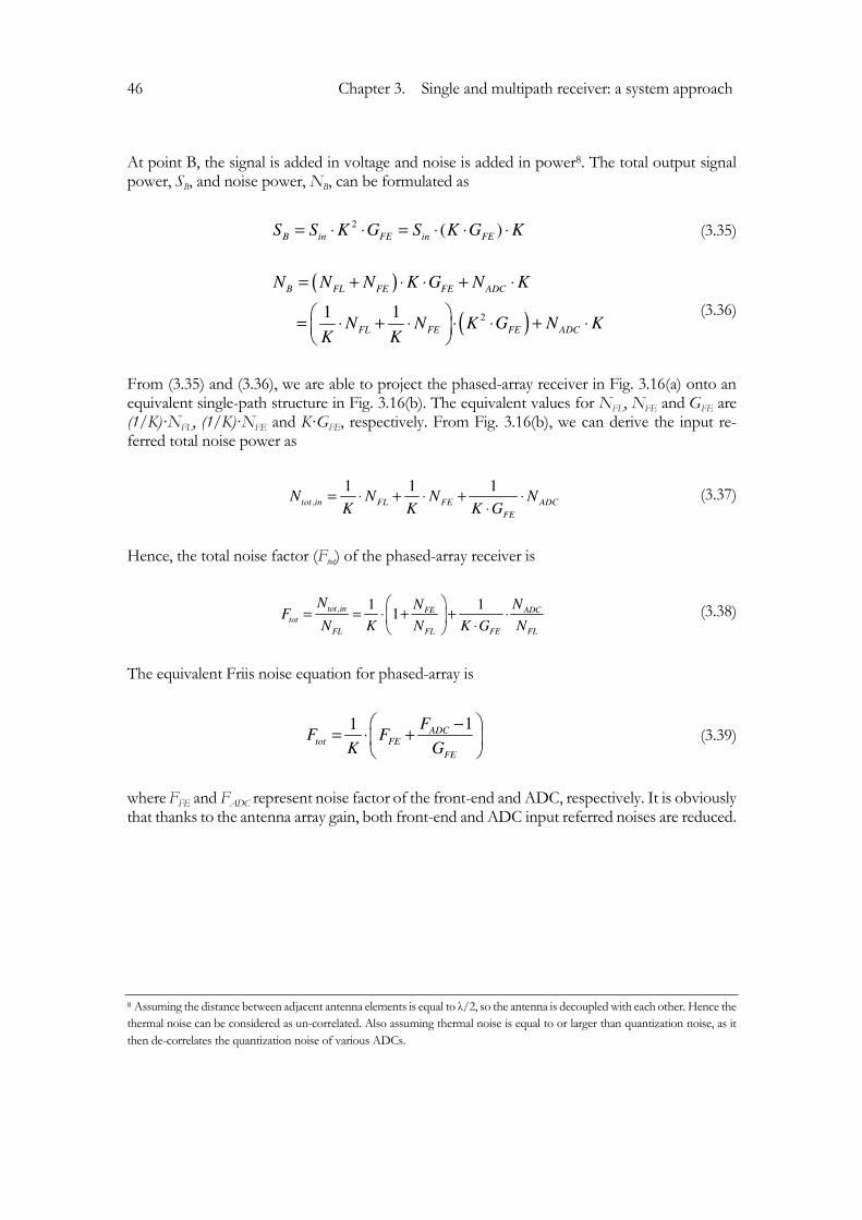
46 Chapter 3. Single and multipath receiver: a system approach
At point B, the signal is added in voltage and noise is added in power8. The total output signal power, SB, and noise power, NB, can be formulated as
2( )B in FE in FES S K G S K G K= ⋅ ⋅ = ⋅ ⋅ ⋅ (3.35)
( )
( )21 1
B FL FE FE ADC
FL FE FE ADC
N N N K G N K
N N K G N KK K
= + ⋅ ⋅ + ⋅
= ⋅ + ⋅ ⋅ ⋅ + ⋅
(3.36)
From (3.35) and (3.36), we are able to project the phased-array receiver in Fig. 3.16(a) onto an equivalent single-path structure in Fig. 3.16(b). The equivalent values for NFL, NFE and GFE are (1/K)·NFL, (1/K)·NFE and K·GFE, respectively. From Fig. 3.16(b), we can derive the input re-ferred total noise power as
,
1 1 1tot in FL FE ADC
FE
N N N NK K K G
= ⋅ + ⋅ + ⋅⋅
(3.37)
Hence, the total noise factor (Ftot) of the phased-array receiver is
, 1 11
tot in ADCFEtot
FL FL FE FL
N NNF
N K N K G N
= = ⋅ + + ⋅
⋅ (3.38)
The equivalent Friis noise equation for phased-array is
11 ADC
tot FE
FE
FF F
K G
−= ⋅ +
(3.39)
where FFE and FADC represent noise factor of the front-end and ADC, respectively. It is obviously that thanks to the antenna array gain, both front-end and ADC input referred noises are reduced.
8 Assuming the distance between adjacent antenna elements is equal to λ/2, so the antenna is decoupled with each other. Hence the
thermal noise can be considered as un-correlated. Also assuming thermal noise is equal to or larger than quantization noise, as it
then de-correlates the quantization noise of various ADCs.

3.5 Digital beam-forming 47
2
FEK G
MULTI
ANTENNA
ADC
OUTPUT
ADC
INPUT
1FEF
K⋅
1FE
NK
⋅
kT BW⋅
,tot inN
totF
totN
FEN∆
ADCK F⋅
ADCK N⋅
Digital
Combination
K K K
Fig. 3.17: Digital phased-array noise power flow diagram
Based on the equivalent single-path structure for digital phased-array shown in Fig. 3.16(b), we can generate the phased-array noise power (mW) flow diagram in Fig. 3.17. Comparing with Fig. 3.10, the difference is that NFE, FFE, and GFE are replaced by (1/K)* NFE, (1/K)* FFE, and K2* GFE, respectively. At the antenna, ADC input, and ADC output front, number K indicates the system has K antennas. Noise of ADC at ADC input front is the sum of ADC noise from K channels, denote by K*NADC and K*FADC. After the ADC output front, the dashed line ‘Digital Combina-tion’ means that the multipath input signals are combined at this place, and forms only one path further on. Similar to (3.16), ∆NFE can be expressed as
tot FE
FE
ADC
F K GN
F
⋅ ⋅∆ = (3.40)
Combining (3.39) and (3.40), the noise figure of front-end and ADC can be derived in (3.41) and (3.42), respectively
1 11FE tot
FE FE
F K FN G
= ⋅ − +
∆ (3.41)
tot FEADC
FE
F K GF
N
⋅ ⋅=
∆ (3.42)

48 Chapter 3. Single and multipath receiver: a system approach
One can see that NFFE has a direct relation with ∆NFE, and NFADC has a reverse relation with ∆NFE. Keeping NFtot, GFE, and K constant, adjusting ∆NFE can result in the trade-off between front-end and ADC noise.
ADCK D⋅
FED∆
kT BW⋅
totD
3ADC
IIP3
FEIIP
3tot
IIP
FEG
FEK D⋅
2K L⋅ADC
I
o u tI
inI
Fig. 3.18: Digital phased-array distortion power flow diagram
Similar to Fig. 3.17, we can generate the phased-array distortion power (mW) flow diagram in Fig. 3.18. From ADC input to Digital Combine front, interference signal power is suppressed by a factor of K2*L, where L is the power rejection factor in (2.39). Both front-end and ADC dis-tortion power are added together from K channels, denoted by K*DFE and K*DADC, respectively. Assuming interferers power Iin dominant the receiver linearity performance, equivalent Friis linearity equation for phased-array is
1
3 3 3
FE
tot FE ADC
K GK
IIP IIP IIP
⋅= + (3.43)
∆DFE in Fig. 3.18 can be expressed as
2
3 1
3
ADCFE
tot FE
IIPD
IIP G K
∆ = ⋅
⋅ (3.44)
Combining (3.43) and (3.44), the IIP3FE and IIP3ADC can be derived in (3.45) and (3.46), respec-tively

3.5 Digital beam-forming 49
33
11
tot
FE
IIP KIIP
D
⋅=
−∆
(3.45)
3 3ADC tot FE FEIIP IIP G K D= ⋅ ⋅ ⋅∆ (3.46)
It shows that IIP3FE has a reverse relation with ∆DFE, and IIP3ADC has a direct relation with ∆DFE. Keeping IIP3tot, and GFE constant, adjusting ∆DFE can result in the trade-off between front-end and ADC linearity. Fig. 3.17 and 3.18 can be combined in Fig. 3.19, which shows the signal, noise and distortion power (mW) flow of a digital phased-array receiver. Note that beam-forming is placed in digital domain, hence the suppression factor L is in the right part of the plane.
FEG
totF
1FE
FK
⋅
1FEN
K⋅
kT BW⋅
,tot inN
totN
FEN∆
3ADCIIP3FEIIP
3totIIP
2
FEK G⋅
ADCK N⋅ FED∆
totD
2K L⋅
ADCK D⋅
FEK D⋅
ADCI
ou tI
inI
inS
ADCS
outS
ADCK F⋅
Fig. 3.19: Digital phased-array signal, noise and distortion power flow diagram

50 Chapter 3. Single and multipath receiver: a system approach
There are two types of power flow in Fig. 3.19,
• The flow of interference signal from Iin increase to IADC with single-path front-end gain GFE. Then from IADC suppressed to Iout due to power rejection factor L.
• The flow of desired signal from Sin increased to Sout, due to signal added in voltage.
3.6 General case of beam-forming
As explained in the previous sections, beam-forming can be implemented in the analog domain or digital domain. Analog beam-forming (ABF) combines the signal from the antennas in the analog domain and relaxes the dynamic range of the following receiver blocks. However, the phase information from each antenna is also lost after the combination. On the other hand, digital beam-forming (DBF) conveys signal amplitude and phase into the digital domain, which provides more flexibility and control of the signal in terms of applying various algorithms. Nevertheless, the hardware replication, especially the power hungry ADCs, will increase the overall power consumption, area and cost.
For a more general case of beam-forming, instead of either analog or digital beam-forming, one can think of a way in between, which means beam-forming is partly done in analog domain, and partly done in digital domain. In section 3.4, Fig. 3.15 shows a signal, noise and distortion power flow diagram of an analog phased-array system, where the signals combine occurs before ADC. In section 3.5, Fig. 3.19 shows a power flow diagram of a digital phased-array system, where the signals combine occurs after ADC. Using properties from both Fig. 3.15 and 3.19, one can de-sign a power flow diagram for general case beam-forming, which is shown in Fig. 3.20.
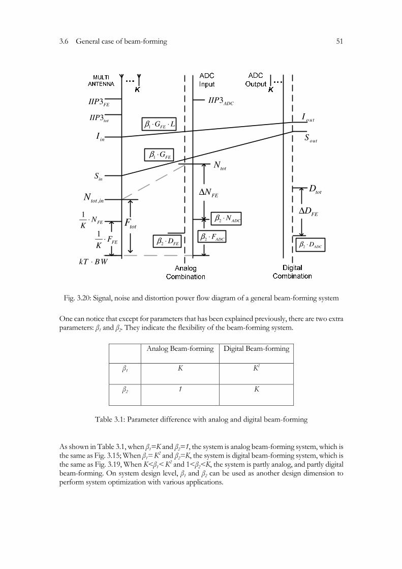
3.6 General case of beam-forming 51
1 FEG Lβ ⋅ ⋅
totF
1FEF
K⋅
1FEN
K⋅
kT BW⋅
,tot inN
totN
FEN∆
3ADC
IIP3FEIIP
3totIIP
2 ADCNβ ⋅
2 ADCDβ ⋅
FED∆
totD
o u tI
inI
inS
outS
2 ADCFβ ⋅2 FE
Dβ ⋅
1 FEGβ ⋅
Fig. 3.20: Signal, noise and distortion power flow diagram of a general beam-forming system
One can notice that except for parameters that has been explained previously, there are two extra parameters: β1 and β2. They indicate the flexibility of the beam-forming system.
Analog Beam-forming Digital Beam-forming
β1 K K2
β2 1 K
Table 3.1: Parameter difference with analog and digital beam-forming
As shown in Table 3.1, when β1=K and β2=1, the system is analog beam-forming system, which is the same as Fig. 3.15; When β1= K2 and β2=K, the system is digital beam-forming system, which is the same as Fig. 3.19, When K<β1< K2 and 1<β2<K, the system is partly analog, and partly digital beam-forming. On system design level, β1 and β2 can be used as another design dimension to perform system optimization with various applications.

52 Chapter 3. Single and multipath receiver: a system approach
3.7 Conclusion
This chapter has presented system approaches to both single- and multi-path receivers. With single-path receiver, a design flow for trade-off between RF front-end and ADC block per-formance by translating ADC parameters into RF domain is introduced. This approach indicates two variables, ∆NFE and ∆DFE, for achieving optimum dynamic range in a receiver chain. As-sociating these variables to the power consumption enables the trade-off between RF and ADC block for minimum overall power consumption. After that, two types of multi-path receiver, namely, analog beam-forming and digital beam-forming are analyzed as a single chain receiver with their equivalent model. It started with analyzing the difference between phased-array and single-chain receivers from noise and linearity perspectives and the result indicates that for both cases, the total noise figures are reduced due to non-correlated noise adding, and the total IIP3 are increased due to interference cancellation. At last, this chapter provided a general case of beam-forming analysis, and two parameters β1 and β2 are introduced to indicate the flexibility of the beam-forming. When K<β1< K2 and 1<β2<K, the system is partly analog, and partly digital beam-forming. On system design level, β1 and β2 can be used as another design dimension to perform system optimization with various applications.

53
Ch ap t e r 4
4 Two-step beam-forming: multip-lexing architecture
A multiplexing phased-array architecture combines K antenna paths into one path by dividing the signal into different time slots. The signals from the antennas are received in rapid succes-sion, one after the other, each using its own time slot. After mixing, filtering, and analog to digital conversion, the multiplexed signal is de-multiplexed in the digital domain, and digital phase shifters are applied to compensate the phase differences for each channel. In the end, signals are combined again in the digital domain, and the desired signal is picked up by means of digital filtering. This chapter presents the concept of multiplexing phased-array architecture and its major properties. The detailed analysis of this architecture is discussed in chapter 5 and 6.
4.1 Multiplexing architecture introduction
Fig. 4.1 shows a flexible phased-array receiver architecture matches with Fig. 1.2. The analog combination block is implemented by an K:1 multiplexer, which chops up the channel into se-

54 Chapter 4. Two-step beam-forming: multiplexing architecture
quential time slices. As such, the phase information from each channel is carried to the digital domain. The analog signal processing block is implemented by a mixer and a band-pass filter. In digital domain, the combined signal is separated again by a de-multiplexer which is synchronized with the multiplexer. After that, the phase difference of each channel is compensated by a digital phase shifter, where the beam-forming algorithms can be applied.
MULf
Sf
loganaBW digital
BW
Fig. 4.1: Multiplexing system structure
The major properties of the multiplexing system can be summarized as the following:
• No analog phase shifter is implemented at the RF front-end. The phase shifter is only implemented in digital domain.
• The multiplexer can be seen as a beam-forming component in itself, because the clock generator generates switching pulses with phase delays. But, assuming the analog filter is not present, then the de-multiplexer in digital domain compensates the previous generated phase delays, and the original input phase information are preserved for the digital phase-shifter.
• The analog band pass filter is used to relax the following ADC design in two aspects. Firstly, ADC bandwidth is relaxed. The band pass filter bandwidth will determine the ADC bandwidth. And secondly, it creates a coarse spatial filter (because of the combina-tion usage with the multiplexer) which filters out the spatial interferences, to relax the ADC dynamic range. The details will be explained in chapter 5.
• The digital phase shifter provides the flexibility to compensate the non-ideal phase in-fluences in the analog path, and formalize the final array patter in digital domain with high speed and accuracy.

4.1 Multiplexing architecture introduction 55
Fig. 4.2 shows the simplified model for multiplexing structure to explain the frequency spectrum transformation from point A to B, where θ is the angle of incidence, BWanalog is the analog filter bandwidth, and Ø is the digital phase compensation. Point A and B are located right after mul-tiplexer and de-multiplexer, respectively. At point A, the frequency spectrum for θ=0° has only one component located in the fundamental tone (n=0). The frequency spectrum for θ≠0° has multiple components located throughout the spectrum. Depending on the condition applied to parameters BWanalog and Ø, the spectrum at point B for different angle of incidence behaves dif-ferently. The detailed explanation of this transformation will be explained in chapter 5.
3Ø1
2
k
K
1
2
k
K
2Ø
Ø
0
θ=0°
θ≠0°
Ø=θθ=0°
θ≠0°
BWanalog=∞
Ø=θ
Ø≠θ
BW≠∞
loganaBW digital
BW
n=0
n=0
n=0
n=0
A B
Fig. 4.2: Simplified model for multiplexing structure to explain the frequency spectrum trans-formation from point A to B.
The time division multiplexing phased-array receiver uses a clock controlled multiplexer to combine K paths into one. The switch-driving waveform is shown in Fig. 4.3. At time slot one, channel one is connected, and all other channels are disconnected. At time slot two, channel two is connected, and all other channels are disconnected, etc. The time slot for each channel is designed to be equal.

56 Chapter 4. Two-step beam-forming: multiplexing architecture
τ ST
Fig. 4.3: Switch driving waveform for multiplexing system
In Fig. 4.3, τ represents the duration for each time slot, and TS represents one period in which all the channels have been connected once. We have
ST K τ= ⋅ (4.1)
1MUL S
S
Kf K f
Tτ= = = ⋅ (4.2)
To recover the signal from each path correctly in the digital domain, the sampling rate for each path (fS) must fulfill the Nyquist sampling theory [64]
2Sf BW> ⋅ (4.3)
where BW is the single side bandwidth of the incoming modulated signal. As a result, the mul-tiplexer sampling rate fMUL can be expressed as
BWKfKf SMUL ⋅>⋅= 2 (4.4)

4.2 Spatial to frequency mapping 57
which means that the larger the signal bandwidth BW, or the larger the antenna number K, the faster the sampling speed fMUL. On the other hand, for a dedicated technology, the sampling speed fMUL has a upper limit, which also limits the incoming signal bandwidth when K is fixed, or limits the total antenna number if the incoming signal bandwidth BW is fixed.
4.2 Spatial to frequency mapping
The phased-array multiplexing architecture can achieve spatial domain to frequency domain mapping in the following way:
• In the spatial domain, the angular information θ (in degrees) at the antenna front is translated to a wave-front time delay ∆t (in second) between adjacent channels.
• In time domain, the time delay ∆t can be modeled (assuming narrow band) as a waveform phase difference φ (in rad) between adjacent channels.
• The multiplexer is acting like a kind of phase modulation. Through the K:1 multiplexing, an input signal with phase difference φ is modulated to the carrier.
• Using Fourier transform, the phase modulated signal is presented in the frequency domain with a unique frequency pattern.
The detailed spatial domain to frequency domain mapping is explained in chapter 5.2.1.
4.3 Two steps of spatial filtering
The phased-array multiplexing architecture can achieve two steps of spatial filtering in the fol-lowing way:
• The coarse spatial filtering is realized by the analog band-pass filter as shown in Fig. 4.1. Because of the unique mapping from spatial to frequency domain, a filter in frequency domain can result in a filter in spatial domain. This filter is used to filter out the spatial interferences far away from the desired angle of incidence, to relax the specification re-quirement for the following ADC. Note that it is called coarse spatial filtering, because it is a coarse-selectivity.
• The final spatial filtering is realized after the digital band-pass filter as shown in Fig. 4.1. It is the place where the final array pattern is formed. After de-multiplexer and phase-shifter,

58 Chapter 4. Two-step beam-forming: multiplexing architecture
the achieved final array pattern is similar to a conventional phased-array pattern. Note that the final selectivity can only be applied within the region that is defined by the coarse-selectivity.
The detailed coarse and final spatial filtering is explained in chapter 5.2 to 5.4.
4.4 Phased-array analog and digital co-design
As previously explained, the design of the phased-array multiplexing architecture can be sepa-rated in two parts: the coarse spatial filtering in analog domain, and the final spatial filtering in digital domain. Hence, the phased-array functionality is achieved by a co-design in the analog and digital domain with different design focus.
• In the analog part, the focus of the design is the coarse spatial filtering bandwidth. If the bandwidth is too small, the final array pattern in the digital domain cannot be achieved. (Note that the final selectivity can only be applied within the region that is defined by the coarse-selectivity.) If the bandwidth is too large, the coarse-selectivity is not effective, and the ADC design specification cannot be relaxed, because of the interference. Hence it is a trade-off, and it is determined by the number of antennas K, the analog filter bandwidth BWa, and the switching frequency fS.
• In the digital part, the focus of the design is on the digital beam-steering speed and ac-curacy. It is determined by the implementation of the digital phase-shifter.
The idea of phased-array analog and digital co-design is to make both analog and digital designs programmable, so that we can achieve phased-array functionality with more flexibility.
4.5 Generalized phased-array system design
With a programmable phased-array structure, the separation between analog and digital beam-forming is not so sharp anymore. Besides the phase-shifter, we can take more design pa-rameters into considerations, so the phased-array functionalities can be achieved partly in analog and partly in digital domain. In chapter 3.6, a generalized beam-forming model is presented. The phased-array multiplexing architecture is one of the realizations of such a generalized beam-forming model.
• From interference point of view, the array pattern is partly formed in analog and partly in digital domain.

4.5 Generalized phased-array system design 59
• From noise point of view, in analog domain, the multiplexing phased-array has a similar structure as analog phased-array, in terms of K:1 combination. Hence the noise behavior is also similar to a analog phased-array. But with such a noise cost, we still keep the flexibility to perform the final phase-steering in the digital domain.
The detailed flow diagram of a multiplexing phased-array is presented in chapter 6.6.

60 Chapter 4. Two-step beam-forming: multiplexing architecture
61
Chap t e r 5
5 Multiplexing architecture, ideal behavior
Fig. 4.1 shows the block diagram of a multiplexing phased-array receiver. The signal is processed in the following different steps: analog switching, analog combining, analog mixing, analog fil-tering, AD conversion, digital switching, digital phase shifting, digital combining, and in the end filtering. In this chapter, we will mathematically analyze this architecture in detail. Section 5.1 discusses the architecture upto the first combination which is the analog combination. The properties of the combined signal will be discussed using traditional phase modulation theory. Based on the result, a new coefficient function Dn will be introduced in section 5.2 to explain the properties of the combined signal. Based on the properties of the combined signal, we introduce a new concept, which is a frequency to space filtering transformation. Section 5.3 discusses the digital part of the architecture. A mathematical analysis is applied to the digital de-multiplexing and phase shifting. After the second combination, in digital domain, the array pattern of the multiplexing architecture is simulated in section 5.4. Section 5.5 concludes what has been dis-cussed in this chapter.

62 Chapter 5. Multiplexing architecture, ideal behavior
5.1 Analog multiplexing
As shown in Fig. 4.1, the multiplexing phased-array architecture starts with transferring signals from multiple channels into one channel. This process can be separated into two steps, namely switching and combining. In this section, we will first introduce the idea of a pulse modulated phased-array signal of a single channel, and then extend the model into multiple channels and the combination of them.
5.1.1 Properties of the switching signal
Switching is a fundamental part of a multiplexing architecture. In time domain, the switching signal can be represented by a square wave, as shown in Fig. 5.1, where TS =1/fS is the period of the pulse train; tS is the starting time delay of the pulse; α1 and α2 are the positive and negative amplitude, respectively; τ is the pulse width of the pulse.
τ
ST
t
( )u t
St
1α
2α0
Fig. 5.1: Switching signal
In one period [0, Ts), u(t) can be expressed as
<≤+
+<≤
<≤
=
SS
SS
S
Ttt
ttt
tt
tu
τα
τα
α
2
1
2 0
)( (5.1)
5.1 Analog multiplexing 63
As we know, this waveform can be represented over (-∞, +∞) by the complex exponential Fourier series as [65]
∑∞=
−∞=
⋅=n
n
tfjn
nSectu
π2)( (5.2)
where n is the harmonic order number, fS=(1/TS), and the complex Fourier coefficients cn can be expressed in two different situations, for n=0,
( )
( )2
21
210
2
00
1
1
αταα
ααατ
τ
+⋅−
=
⋅+⋅+⋅⋅=
⋅⋅=
∫∫∫
∫
+
+
S
T
t
t
t
t
S
T
S
T
dtdtdtT
dttuT
c
S
S
S
S
S
S
(5.3)
and for n≠0,
( )
( )( ) ( )
2
0
2 2 2
2 1 20
21 2
1
1
sin
SS
S S SS S S
S S
S S
Tjn f t
n
S
t t Tjn f t jn f t jn f t
t tS
jn f t
S
c u t e dtT
e dt e dt e dtT
e n fn
π
τπ π π
τ
π τ
α α α
α απ τ
π
− ⋅
+− ⋅ − ⋅ − ⋅
+
− +
= ⋅ ⋅ ⋅
= ⋅ ⋅ ⋅ + ⋅ ⋅ + ⋅ ⋅
−= ⋅ ⋅ ⋅
⋅
∫
∫ ∫ ∫ (5.4)
Substituting cn from (5.3) and (5.4) into (5.2), u(t) can be further expressed as
( ) ( ) ( )
⋅⋅⋅
⋅−
+
+
⋅−=
+=
∑
∑∑
∞=
≠−∞=
⋅+⋅−
∞=
≠−∞=
⋅
=
⋅
n
nn
tfjntfjnS
S
n
nn
tfjn
n
n
tfjn
n
SSS
SS
een
fn
T
ecectu
0
2221
2
21
0
2
0
2
sin
)(
πτπ
ππ
τπ
π
ααα
ταα
(5.5)
Fig. 5.2 shows the amplitude part of the frequency spectrum of u(t), for the positive part of the frequency axis.

64 Chapter 5. Multiplexing architecture, ideal behavior
MULf
SS
Tf
τ⋅
2S
S
Tf
τ⋅
Sf 2
Sf
Fig. 5.2: Amplitude part of the frequency spectrum of u(t).
At each integer multiples of harmonic TS/τ, the envelope of u(t) drops to zero.
5.1.2 Pulse modulation
According to communication theory [66], any physical band-pass waveform can be represented by
( ) tfj Cetmtsπ2
Re)( ⋅= (5.6)
Where Re. denotes the real part of ., m(t) is called the complex envelope of s(t), and fC is the associated carrier frequency. In a phased-array receiving system, the signals arriving in each channel are the original signal with different phase shifts. The signals received by the k-th an-tenna element can be written as
( ) 2 ( 1)( ) Re Cj f t k
ks t m t e
π ϕ+ −= ⋅ (5.7)
where φ is the differential carrier phase change between two consecutive antenna elements. The value of φ (rad) can be written in the form
( ) ( )2
sin sindπ
ϕ θ π θλ
= ⋅ = ⋅ (5.8)

5.1 Analog multiplexing 65
where d is the distance between two adjacent antennas, and assuming d=λ/2; λ is the wavelength of the incoming signal; θ is the incoming space angle in degrees. Furthermore, in a multiplexing phased-array receiving system, the signal in each channel is modulated by a pulse function u(t) which is described in equation (5.5). The behavior model of this modulation is shown in Fig. 5.3.
2
1Re ( ) ( )Cj f tm t e u t
π ⋅ ⋅
2
2Re ( ) ( )Cj f t jm t e u t
π ϕ+ ⋅ ⋅
2 ( 1)Re ( ) ( )Cj f t j K
Km t e u tπ ϕ+ − ⋅ ⋅
2 ( 1)Re ( ) ( )Cj f t j k
km t e u t
π ϕ+ − ⋅ ⋅
Fig. 5.3: Model of multiplexing phased-array pulse modulation
From Fig. 5.3, in general situation, the modulated signal in the k-th channel can be expressed as
( )
[ ]
2 ( 1)
2
,
2 2 2 2( 1) ( 1)
, ,
( ) Re ( )
( ) cos 2 ( 1)
1( )
2
C
S
C S C S
j f t j k
k k
njn f t
C n k
n
n nj f t jn f t j f t jn f tj k j k
n k n k
n n
positive frequency n
x t m t e u t
m t f t k c e
m t e e c e e e c e
π ϕ
π
π π π πϕ ϕ
π ϕ
⋅ + −
=∞⋅
=−∞
=∞ =∞⋅ ⋅ − ⋅ ⋅− − −
=−∞ =−∞
= ⋅ ⋅
= ⋅ + − ⋅
= ⋅ ⋅ ⋅ + ⋅ ⋅
∑
∑ ∑
egative frequency
(5.9)
where cn,k is the complex Fourier coefficients for the k-th channel. In the frequency domain, the modulated signal has both positive and negative frequencies. Here, we consider only positive frequencies. Substituting cn from (5.3) and (5.4) into (5.9), xk(t)|positive can be expressed as
66 Chapter 5. Multiplexing architecture, ideal behavior
( )
( ) ( ),
2 2( 1)
,
2 1 2( 1)
2
22 2( 1) 1 2
1( ) ( )
2
1( ) ( 0)
2
1( ) sin
2
C S
C
S S k kC S
nj f t jn f tj k
k n kpositiven
j f t kj k
S
jn f tj f t jn f tj k
S k
x t m t e e c e
m t e e nT
m t e e n f e en
π πϕ
π ϕ
π τπ πϕ
α α τα
α απ τ
π
=∞⋅ ⋅−
=−∞
⋅ −
− ⋅ +⋅ ⋅−
= ⋅ ⋅ ⋅
− ⋅ = ⋅ ⋅ ⋅ + =
−+ ⋅ ⋅ ⋅ ⋅ ⋅ ⋅ ⋅
∑
0
( 0)n
nn
n=∞
=−∞≠
≠
∑
(5.10)
The above equation can be expanded into different frequency components.
5.1 Analog multiplexing 67
Table 5.1 lists the components until the n=±4 harmonic.
Number Frequency Component
n=0 fC ( ) 21 2 ( 1)
2
1( )
2Cj f tk j k
S
m t e eT
πϕα α τα ⋅−− ⋅
⋅ + ⋅ ⋅
n=1 fC+fS ( ) ,( 1) 2 2 ( )1 21( ) sin
2
S S k S k C Sj k f t f j f f t
S km t f e e
ϕ π π τ πα απ τ
π
− − − + −⋅ ⋅ ⋅ ⋅
n=2 fC+2fS ( ) ,( 1) 4 2 2 ( 2 )1 21( ) sin 2
2 2
S S k S k C Sj k f t f j f f t
S km t f e eϕ π π τ πα α
π τπ
− − − + −⋅ ⋅ ⋅ ⋅
n=3 fC+3fS ( ) ,( 1) 6 3 2 ( 3 )1 21( ) sin 3
2 3
S S k S k C Sj k f t f j f f t
S km t f e eϕ π π τ πα α
π τπ
− − − + −⋅ ⋅ ⋅ ⋅
n=4 fC+4fS ( ) ,( 1) 8 4 2 ( 4 )1 21( ) sin 4
2 4
S S k S k C Sj k f t f j f f t
S km t f e eϕ π π τ πα α
π τπ
− − − + −⋅ ⋅ ⋅ ⋅
n=-1 fC-fS ( ) ,( 1) 2 2 ( )1 21( ) sin
2
S S k S k C Sj k f t f j f f t
S km t f e eϕ π π τ πα α
π τπ
− + + − −⋅ ⋅ ⋅ ⋅
n=-2 fC-2fS ( ) ,( 1) 4 2 2 ( 2 )1 21( ) sin 2
2 2
S S k S k C Sj k f t f j f f t
S km t f e eϕ π π τ πα α
π τπ
− + + − −⋅ ⋅ ⋅ ⋅
n=-3 fC-3fS ( ) ,( 1) 6 3 2 ( 3 )1 21( ) sin 3
2 3
S S k S k C Sj k f t f j f f t
S km t f e eϕ π π τ πα α
π τπ
− + + − −⋅ ⋅ ⋅ ⋅
n=-4 fC-4fS ( ) ,( 1) 8 4 2 ( 4 )1 21( ) sin 4
2 4
S S k S k C Sj k f t f j f f t
S km t f e eϕ π π τ πα α
π τπ
− + + − −⋅ ⋅ ⋅ ⋅
Table 5.1: Component expansion of the k-th channel pulse modulated signal
Each frequency component is uniquely defined, and can be identified by four different proper-ties: frequency component, harmonic number, amplitude, and phase. Closely investigating which parameters of the square wave (Fig. 5.1) and incoming signal (Fig. 5.3) contribute to the above frequency spectrum, we can break equation (5.10) down into three different properties: fre-

68 Chapter 5. Multiplexing architecture, ideal behavior
quency, amplitude, and phase. Assuming a normalized case, 0.5*|m(t)|=1 in (5.10), we can list how these properties are influenced:
• Parameters that can influence the frequency: fC; fS; n
• Parameters that can influence the amplitude: α1; α2; fS; τk
• Parameters that can influence the phase: K; φ; fS; τk; tS,k
The square wave amplitudes (α1, α2) directly relate to the component amplitude. The channel number (k), phase difference between two adjacent channel (φ), and starting time delay of the pulse (tS,k) directly relate to the component phase. Amplitude and phase are correlated by fS and τk. In frequency domain, summing all the channels means summing of all spectrum components from each frequency of all channels. With a given system application target in mind, we can design the above mentioned parameters such that the properties of the summed signal are as needed. For example, in [28], these parameters are designed to reach maximum amplitude at frequency fC-fS.
5.1.3 Combination in the analog domain
In a multiplexing receiver system, the channels are conducting one after each other, sequentially. When one channel is conducting, other channels must be isolated. Moreover, the conducting time during of each channel is evenly distributed in period TS. Fig. 5.4 describes such a square wave.

5.1 Analog multiplexing 69
1τ
,2St
1α
2α0
,S kt
kτ
ST
,S Kt
Kτ
2τ
Fig. 5.4: Multiplexing pulses
For simplicity, assuming all paths τk equal to 1/(K·fS), and assuming also α1=1, α2=0, tS,1=0/(K·fS),
tS,2=1/(K·fS), tS,k=(k-1)/(K·fS), tS,K=(K-1)/(K·fS), equation (5.10) simplifies to xk(t)|equal-paths as
2 2( 1)
,
2 ( 1)
2 1
2 2( 1)
0
1( ) ( )
2
1 1( ) ( 0)
2
1 1( ) sin
2
C S
C
C S
nj f t jn f tj k
k n kequal pathsn
j f t j k
kn jnj f t jn f tj k K
nn
x t m t e e c e
m t e e nK
nm t e e e e
n K
π πϕ
π ϕ
ππ πϕ π
π
=∞⋅ ⋅−
−=−∞
⋅ −
− =∞ − ⋅ ⋅ ⋅−
=−∞≠
′= ⋅ ⋅ ⋅
= ⋅ ⋅ ⋅ =
⋅ + ⋅ ⋅ ⋅ ⋅ ⋅ ⋅
∑
∑ ( 0)n
≠
(5.11)
Note that for this specific situation of all equal paths, we use c’n,k as the complex Fourier coeffi-cients. Note also that φ is the differential carrier phase change between two consecutive antenna elements. As shown in Fig. 5.3, the pulse modulated signals from all channels are summed to-gether. Substituting φ from (5.8) into (5.11), the summed signal in the time domain can be ex-pressed as
( )( 1) sin2 2
,
1 1
1( ) ( ) ( )
2C S
K n Kj kj f t jn f t
sum k n kequal pathk n k
x t x t m t e c e eπ θπ π
=∞− ⋅ ⋅
−= =−∞ =
′= = ⋅ ⋅ ⋅ ⋅
∑ ∑ ∑ (5.12)

70 Chapter 5. Multiplexing architecture, ideal behavior
5.2 Spatial to frequency mapping
Define Dn as the coefficient function of the n-th order harmonic
( )( 1) sin
,
1
( , )K
j k
n n k
k
D K c eπ θθ − ⋅
=
′= ⋅∑ (5.13)
Dn is determined by two variables, K and θ, in which K is the number of antennas and θ is the incoming signal angle of incidence. Substituting (5.13) into (5.12), xsum(t) can be expressed as
2 21( ) ( ) ( , )
2C S
nj f t jn f t
sum n
n
x t m t e D K eπ πθ
=∞⋅
=−∞
= ⋅ ⋅ ⋅∑ (5.14)
Taking the Fourier transform of (5.14), we obtain
1( ) ( ) ( , ) ( )
2
n
sum n C S
n
X f M f D K f n fθ δ=∞
=−∞
= ⋅ ⋅ − ⋅∑ (5.15)
The above equation (5.15) indicates that the frequency spectrum of xsum(t) is modulated by the incoming signal angle of incidence θ. In another word, a multiplexing phased-array architecture transfers space angle information into frequency information. This property will be discussed in detail in section 5.2.1.
5.2.1 Space to frequency mapping coefficient Dn
To understand the summed phase modulated signal xsum(t), it is important to understand function Dn(K,θ) first. In the following analysis, we assume four antennas, normalized input signal, and normalized and equal paths, we get: K=4, τ4=1/(4·fS), α1=1, α2=0, tS,1=0/(4·fS), tS,2=1/(4·fS), tS,3=2/(4·fS), tS,4=3/(4·fS; 0.5*|m(t)|=1. Taking all these assumptions into account, the summed signal in (5.12) can be re-written as
( )4 4
( 1) sin2 2
,
1 1
( ) ( ) C S
nj kj f t jn f t
sum k n kequal pathk n k
x t x t e c e eπ θπ π
=∞− ⋅ ⋅
−= =−∞ =
′= = ⋅ ⋅ ⋅
∑ ∑ ∑ (5.16)
From (5.13), the Dn(K,θ) for four antennas can be expressed as

5.2 Spatial to frequency mapping 71
( )4
( 1) sin
,
1
(4, )j k
n n k
k
D c eπ θθ − ⋅
=
′= ⋅∑ (5.17)
Substituting equation (5.3) and (5.4) into (5.17), and expending the amplitude of Dn(4,θ) and ignore the phase component, we have
( )
( ) ,
4( 1) sin
1
4( 1) sin 2
4
1
10
4(4, )
1sin 0
4
S S k
j k
k
n nj j k n f t
k
e n
Dn
e e nn
π θ
ππ θ π
θπ
π
−
=
− − ⋅ − ⋅ ⋅
=
⋅ =
=
⋅ ⋅ ⋅ ≠
∑
∑ (5.18)
Substituting φ from (5.8) into (5.18), table 5.2 extends the relation of harmonic number n and |Dn(4,θ)|, until the ±4th harmonic.
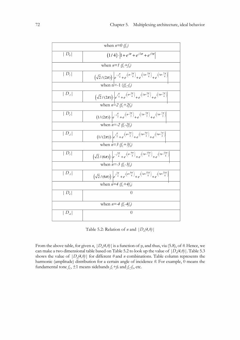
72 Chapter 5. Multiplexing architecture, ideal behavior
when n=0 (fC)
| D0| ( ) 2 31/ 4 1 j j je e e
ϕ ϕ ϕ⋅ + + +
when n=1 (fC+fS)
| D1| ( )
3 5 72 3
4 4 442 / (2 )j j jj
e e e e
π π ππ ϕ ϕ ϕ
π
− − −− ⋅ + + +
when n=-1 ((fC-fS)
| D-1| ( )
3 5 72 3
4 4 442 / (2 )j j jj
e e e e
π π ππ ϕ ϕ ϕ
π
+ + + ⋅ + + +
when n=2 (fC+2fS)
| D2| ( )
3 5 72 3
2 2 221/ (2 )j j jj
e e e e
π π ππ ϕ ϕ ϕ
π
− − −− ⋅ + + +
when n=-2 (fC-2fS)
| D-2| ( )
3 5 72 3
2 2 221/ (2 )j j jj
e e e e
π π ππ ϕ ϕ ϕ
π
+ + + ⋅ + + +
when n=3 (fC+3fS)
| D3| ( )
9 15 213 2 34 4 442 / (6 )
j j jj
e e e e
π π ππ ϕ ϕ ϕ
π
− − −− ⋅ + + +
when n=-3 (fC-3fS)
| D-3| ( )
9 15 213 2 34 4 442 / (6 )
j j jj
e e e e
π π ππ ϕ ϕ ϕ
π
+ + + ⋅ + + +
when n=4 (fC+4fS)
| D4| 0
when n=-4 (fC-4fS)
| D-4| 0
Table 5.2: Relation of n and |Dn(4,θ)|
From the above table, for given n, |Dn(4,θ)| is a function of φ, and thus, via (5.8), of θ. Hence, we can make a two dimensional table based on Table 5.2 to look up the value of |Dn(4,θ)|. Table 5.3 shows the value of |Dn(4,θ)| for different θ and n combinations. Table column represents the harmonic (amplitude) distribution for a certain angle of incidence θ. For example, 0 means the fundamental tone fC, ±1 means sidebands fC+fS and fC-fS, etc.

5.2 Spatial to frequency mapping 73
Θ
n
0 10 20 30 40 50 60 70 80 90
-8 - - - - - - - - - -
-7 - 0.058 0.110 0.129 0.113 0.079 0.044 0.019 0.004 -
-6 - 0.049 0.052 - 0.078 0.147 0.189 0.208 0.212 0.212
-5 - 0.046 0.039 - 0.036 0.049 0.040 0.022 0.006 -
-4 - - - - - - - - - -
-3 - 0.136 0.256 0.300 0.264 0.184 0.103 0.044 0.010 -
-2 - 0.147 0.155 - 0.234 0.441 0.568 0.622 0.636 0.637
-1 - 0.229 0.194 - 0.180 0.245 0.200 0.108 0.030 -
0 1.000 0.823 0.409 - 0.231 0.267 0.191 0.093 0.024 -
1 - 0.407 0.767 0.900 0.791 0.552 0.309 0.131 0.031 -
2 - 0.147 0.155 - 0.234 0.441 0.568 0.622 0.636 0.637
3 - 0.076 0.065 - 0.060 0.082 0.067 0.036 0.010 -
4 - - - - - - - - - -
5 - 0.081 0.154 0.180 0.158 0.110 0.062 0.026 0.006 -
6 - 0.049 0.052 - 0.078 0.147 0.189 0.208 0.212 0.212
7 - 0.033 0.028 - 0.026 0.035 0.029 0.015 0.004 -
8 - - - - - - - - - -
Table 5.3: Values of |Dn(4,θ)| with different θ and n combinations. The dashed line (within) indicates the minimum required harmonics to have at least 90% of total power.
The dashed line (within) indicates the minimum required harmonics to have at lease 90% (as an example) of total power for a certain angle of incidence θ. For example, if θ=30°, 0.92=0.81 has not reached 90% of total power; 0.92+0.32=0.9 has reached exactly 90% of total power, so the dashed line is drawn at n=±3. From the above analysis, |Dn(4,θ)| has the property of
),4(),4( θθ nn DD =−− (5.19)
Moreover, at even harmonic number, when n=0, 2, 4, 6, 8…
),4(),4(),4( θθθ −== −− nnn DDD (5.20)

74 Chapter 5. Multiplexing architecture, ideal behavior
(5.19) and (5.20) is also true for other k values. So we have
)6,4,2(),4(),4(),4(
),4(),4(
=−==
=−
−−
−
nDDD
DD
nnn
nn
θθθ
θθ (5.21)
Fig. 5.5 shows the spectrum of |xsum(t)| with incidence angels of 0, 30, 60, 90 degree.

5.2 Spatial to frequency mapping 75
Cf
sumX
Cf
C Sf f+
C Sf f−
Cf
Cf
C Sf f+C Sf f−
sumX
sumX
sumX
Fig. 5.5: Amplitude part of the spectrum of Xsum(f) for (a) θ=0° (b) θ=10° (c) θ=30° (d) θ=60°

76 Chapter 5. Multiplexing architecture, ideal behavior
For different angle of incidence, the spectrum looks differently. At 0 degree, the peak is centered at fC; at 10 degree, the energy is spreading from fC to fC+fS and fC-fS; at 30 degree, the peak is centered at fC+fS, and energy of fC goes to zero. At 60 degree, the energy is spreading to many harmonics in the spectrum. The spectrum of xsum(t) is phase modulated. As section 4.2 explained, a multiplexing phased-array architecture transfers space angle information into frequency in-formation. Furthermore, there is a unique translation from incoming angle of incidence θ to frequency spectrum pattern.
5.2.2 Translation from voltage to power domain, Dn to Pxn
Power in a sinusoidal signal depends only on its amplitude, and is independent of frequency and phase [67]. Remember that in section 2.2, we have discussed in (2.24) that the power of the carrier is spread over the various side components as a function of θ. Hence, we also have
2( , ) 1
n
n
D K θ∞
=−∞
=∑ (5.22)
Define Pxn(K,θ) as the power contained in the n-th pair of side frequency
2
0 0
2 2
( , ) ( , ) 0
( , ) ( , ) ( , ) 1n n n
Px K D K n
Px K D K D K n
θ θ
θ θ θ−
= =
= + ≥ (5.23)
Thus, (5.22) can also be written as
0
( , ) 1n
n
Px K θ∞
=
=∑ (5.24)
Note that (5.24) does not mean physically adding the power. It is a power property indication over all harmonics. Table 5.4 shows the value of Pxn(K,θ) with different θ and n combination, when K=4. Table row represents the harmonic power distribution for a certain angle of inci-dence θ. For example, 0 means the fundamental tone fC, 1 means sidebands fC±fS, etc.
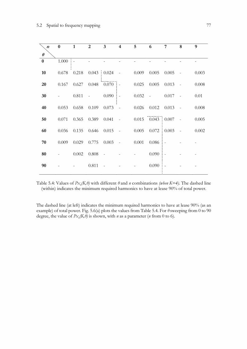
5.2 Spatial to frequency mapping 77
n
θ
0 1 2 3 4 5 6 7 8 9
0 1.000 - - - - - - - - -
10 0.678 0.218 0.043 0.024 - 0.009 0.005 0.005 - 0.003
20 0.167 0.627 0.048 0.070 - 0.025 0.005 0.013 - 0.008
30 - 0.811 - 0.090 - 0.032 - 0.017 - 0.01
40 0.053 0.658 0.109 0.073 - 0.026 0.012 0.013 - 0.008
50 0.071 0.365 0.389 0.041 - 0.015 0.043 0.007 - 0.005
60 0.036 0.135 0.646 0.015 - 0.005 0.072 0.003 - 0.002
70 0.009 0.029 0.775 0.003 - 0.001 0.086 - - -
80 - 0.002 0.808 - - - 0.090 - - -
90 - - 0.811 - - - 0.090 - - -
Table 5.4: Values of Pxn(K,θ) with different θ and n combinations (when K=4). The dashed line (within) indicates the minimum required harmonics to have at lease 90% of total power.
The dashed line (at left) indicates the minimum required harmonics to have at lease 90% (as an example) of total power. Fig. 5.6(a) plots the values from Table 5.4. For θ sweeping from 0 to 90 degree, the value of Pxn(K,θ) is shown, with n as a parameter (n from 0 to 6).

78 Chapter 5. Multiplexing architecture, ideal behavior
Fig. 5.6: Pxn(K,θ) as a function of θ, n=0,1,2,3,4,5,6 (a) when K=4, (b) when K=16.
Table 5.4 and Fig. 5.6(a) show that at different angles of incidence, the energy concentrates in different side frequencies. For example, at 0 degree, all energies are stored in n=0, which is the fundamental frequency. At 30 degree, 81% of the energies are stored in n=1, and the rest of the energies are only stored in the odd harmonics. At 90 degree, 81% of the energies are stored in n=2, and the rest of the energies are only stored in the even harmonics. The above properties give the translation from space/angle difference into frequencies spectrum/energy difference.
Fig. 5.6(b) again shows the Pxn(K,θ) plot, but now for 16 antennas. Comparing with Fig. 5.6(a), the side frequency energy is more concentrated around the corresponding spatial angle, which indicates a better spatial resolution.

5.2 Spatial to frequency mapping 79
5.2.3 Coarse beam pattern RxN by frequency selectivity
The normalized power sum of the first N pairs of harmonics is given by
0
2 2 2
0
1
( , ) ( , )
( , ) ( , ) ( , )
N
N n
n
N
n n
n
Rx K Px K
D K D K D K
θ θ
θ θ θ
=
−=
=
= + +
∑
∑ (5.25)
Note that (5.25) does not mean physically adding the power. It is a power property indication over harmonic pairs up until number N. For example, in case of four antenna elements (K=4), and 10° of angle of inciedence (θ=10°)
)3(963.0
)2(939.0
)1(896.0
)0(678.0
32103
2102
101
00
==+++=
==++=
==+=
===
NPxPxPxPxRx
NPxPxPxRx
NPxPxRx
NPxRx
(5.26)
Following (5.26), we can mark in Table 5.3 and 5.4 dashed line representing the boundary of the minimum required harmonics to have at lease 90% of total power. Two plots of RxN(K,θ) (in dB) as a function of θ are shown in Fig. 5.7.

80 Chapter 5. Multiplexing architecture, ideal behavior
Fig.5.7: RxN(K,θ) as a function of θ, N=0,1,2,3, (a) when K=4, (b) when K=16.
From Fig. 5.7(a), one can notice that the array coarse-pattern looks differently for various N. If N increases, the array coarse-pattern in space becomes less selective, meaning less spatial filtering effect. Note that N denotes the first N pairs of sideband frequencies which are preserved after analog band-pass filtering, as in (5.25), which represent the effect of the frequency filter. Hence, the above figure shows that a filter in the frequency domain results in a filter in space domain. This phenomenon is shown more clearly in Fig. 5.8.
Fig. 5.7(b) again shows the Rxn(K,θ) plot, but for 16 antennas. Comparing with Fig. 5.7(a), with we see that for equal step of filter bandwidth increase in frequency domain, the spatial filter bandwidth is increasing with better resolution. It confirms our analysis in Fig. 5.6.
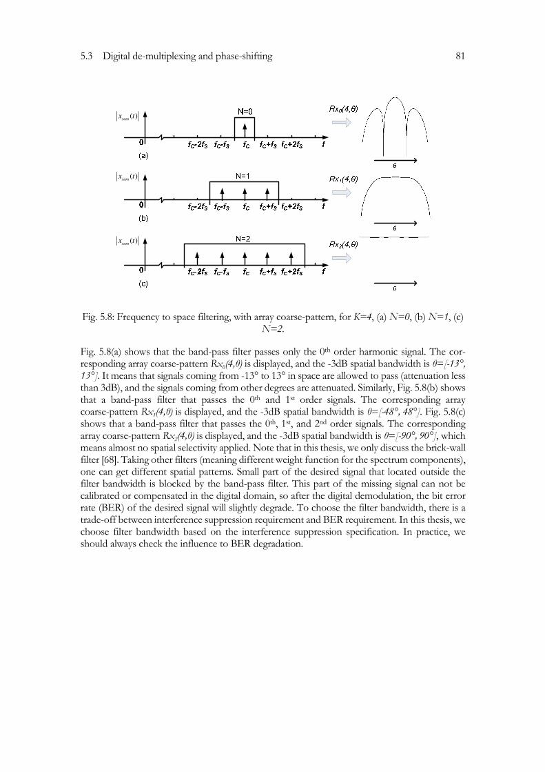
5.3 Digital de-multiplexing and phase-shifting 81
( )sum
x t
( )sum
x t
( )sum
x t
Fig. 5.8: Frequency to space filtering, with array coarse-pattern, for K=4, (a) N=0, (b) N=1, (c) N=2.
Fig. 5.8(a) shows that the band-pass filter passes only the 0th order harmonic signal. The cor-responding array coarse-pattern Rx0(4,θ) is displayed, and the -3dB spatial bandwidth is θ=[-13°, 13°]. It means that signals coming from -13° to 13° in space are allowed to pass (attenuation less than 3dB), and the signals coming from other degrees are attenuated. Similarly, Fig. 5.8(b) shows that a band-pass filter that passes the 0th and 1st order signals. The corresponding array coarse-pattern Rx1(4,θ) is displayed, and the -3dB spatial bandwidth is θ=[-48°, 48°]. Fig. 5.8(c) shows that a band-pass filter that passes the 0th, 1st, and 2nd order signals. The corresponding array coarse-pattern Rx2(4,θ) is displayed, and the -3dB spatial bandwidth is θ=[-90°, 90°], which means almost no spatial selectivity applied. Note that in this thesis, we only discuss the brick-wall filter [68]. Taking other filters (meaning different weight function for the spectrum components), one can get different spatial patterns. Small part of the desired signal that located outside the filter bandwidth is blocked by the band-pass filter. This part of the missing signal can not be calibrated or compensated in the digital domain, so after the digital demodulation, the bit error rate (BER) of the desired signal will slightly degrade. To choose the filter bandwidth, there is a trade-off between interference suppression requirement and BER requirement. In this thesis, we choose filter bandwidth based on the interference suppression specification. In practice, we should always check the influence to BER degradation.

82 Chapter 5. Multiplexing architecture, ideal behavior
5.3 Digital de-multiplexing and phase-shifting
Fig. 5.5 shows that the multiplexing phased-array architecture translates the input signal for each angle of incidence θ to a specific frequency spectrum pattern. Fig. 5.8 shows that a filter in frequency domain results in a filter in space domain and hence forms the array coarse-pattern. Fig. 5.9 shows how the signal is further processed in the digital domain. First, the signal is de-multiplexed from one path back to four paths, and then these four signals are phase shifted according to the desired viewing angle and combined. At last, a band-pass filter is used to clean up the frequency spectrum.
Fig. 5.9: Signal processing in digital domain
In practice, the summed multiplexed signal from (5.14) passes through the mixer, the filter, and the ADC to reach at the input of de-multiplexer. To simplify the analysis, we assume a norma-lized situation, 0.5*|m(t)|=1, and the transfer functions of the mixer, the filter, and the ADC equal to one. So the complex envelope of the input signal is Dn(K,θ), as shown in Fig. 5.9. The input signal is further processed by de-multiplexer and digital phase shifter. Note that the de-multiplexer is using the same switching frequency fS as the multiplexer. Fig. 5.10 (a)-(e) shows the frequency mixing of each input harmonic component due to de-multiplexing. This process can be understood by the following steps: First, due to de-multiplexing, the frequency compo-nents for each channel at the de-multiplexer input are mixing to other locations with step size fS. Next, the digital phase delay component (per channel) applies a desired phase shift to the fun-damental tone in order to add them in-phase (n=0). Thirdly, the phase adjusted fundamental tones from the previous step are added in-phase (per channel). And finally, fundamental com-ponents from all four channels are added together.

5.3 Digital de-multiplexing and phase-shifting 83
0 1 2 3 4-1-2-3-4Harmonic
Order
0 1 2 3 4-1-2-3-4
0 1 2 3 4-1-2-3-4
0 1 2 3 4-1-2-3-4
0 1 2 3 4-1-2-3-4
(c)
(b)
(a)
(d)
(e)
( )1,ky t−
( )0,ky t
( )2,ky t−
( )1,ky t
( )2,ky t
Fig. 5.10: Frequency mixing and spectrum reformation of one channel, (a) n=-2 (b) n=-1 (c) n=0 (d) n=1 (e) n=2

84 Chapter 5. Multiplexing architecture, ideal behavior
For example, at Fig. 5.10(a), the n=-2 component is transferred to:
• the -4th order component via the -2nd (n=-2) harmonic term
• the -3rd order component via the -1st (n=-1) harmonic term
• the -2nd order component via the DC term
• the -1st order component via the 1st (n=1) harmonic term
• the fundamental component via the 2nd (n=2) harmonic term
of the switching function in (5.5). The same frequency mixing mechanism applies to input harmonic components n=-1, n=0, n=1, and n=2 in Fig. 5.10(b), (c), (d), and (e), respectively. However, not all the mixing products are of interest. The digital phase shifters are designed for maximizing the signal amplitude at the fundamental frequency (n=0). So only the mixing products which fall into the fundamental frequency needs to be further processed, as highlighted in Fig. 5.10. Note that the above figure only shows the mixing result of one channel. In case of K channels, the above analysis happens K times and the K results are then summed together. In Fig. 5.9, yn,k(t) is defined as the complex envelope after mixing the n-th harmonic component to the fundamental frequency (n=0) form the k-th channel. For example, after frequency mixing in Fig. 5.10(a), the complex envelope at the fundamental frequency (n=0) is y-2,k(t). Table 5.5 displays a two dimensional parameter matrix, assuming the number of channels is four (K=4). y-2,sum(t) means the sum of the fundamental tones (n=0) from 4 channels, from which the fundamental tone is converted from n=-2 harmonic for each channel. This definition can be extended for all other yn,sum(t). The column of Table 5.5 is matched to the Fig. 5.10 explanation.
k n
1 2 3 4 sum
n=-2 y-2,1(t) y-2,2(t) y-2,3(t) y-2,4(t) y-2,sum(t)
n=-1 y-1,1(t) y-1,2(t) y-1,3(t) y-1,4(t) y-1,sum(t)
n=0 y0,1(t) y0,2(t) y0,3(t) y0,4(t) y0,sum(t)
n=1 y1,1(t) y1,2(t) y1,3(t) y1,4(t) y1,sum(t)
n=2 y2,1(t) y2,2(t) y2,3(t) y2,4(t) y2,sum(t)
Table 5.5: Parameter matrix of yn,k(t), when K=4

5.3 Digital de-multiplexing and phase-shifting 85
Taking n=-2 as an example, y-2,k(t) can be express as
0
2,1 2 2,1
1
2,2 2 2,2
2
2,3 2 2,3
3
2,4 2 2,4
( ) (4, )
( ) (4, )
( ) (4, )
( ) (4, )
j
j
j
j
y t D c e
y t D c e
y t D c e
y t D c e
γ
γ
γ
γ
θ
θ
θ
θ
⋅
− −
⋅
− −
⋅
− −
⋅
− −
′= ⋅ ⋅
′= ⋅ ⋅
′= ⋅ ⋅
′= ⋅ ⋅
(5.27)
where γ is the digital phase shifter in radians. Applying the definition of Dn in (5.17), we get
( )4
( 1) sin
,
1
(4, )j k
n n k
k
D c eπ φφ − ⋅
=
′= ⋅∑ (5.28)
Let γ=B*sin(Ø), we get
( )
2, 2,1 2,2 2,3 2,4
4( 1) sin
2 2,
1
2 2
( ) ( ) ( ) ( ) ( )
(4, )
(4, ) (4, )
sum
j k
k
k
y t y t y t y t y t
D c e
D D
π φθ
θ φ
− − − − −
− ⋅
−=
−
= + + +
′= ⋅ ⋅
= ⋅
∑ (5.29)
Applying the same calculation to Fig. 5.10 (b), (c), (d), and (e) results in
1, 1 1
0, 0 0
1, 1 1
2, 1 2
( ) (4, ) (4, )
( ) (4, ) (4, )
( ) (4, ) (4, )
( ) (4, ) (4, )
sum
sum
sum
sum
y t D D
y t D D
y t D D
y t D D
θ φ
θ φ
θ φ
θ φ
− −
−
−
= ⋅
= ⋅
= ⋅
= ⋅
(5.30)
If we preserve all sidebands power (extend to infinite) and transfer them to the fundamental frequency (n=0) through de-multiplexing, the complete input carrier power is preserved. If the desired phase delay is applied to each path, at the fundamental tone (n=0), all folded frequency components are added in phase, and at other location (n≠0), all folded frequency components are added out-of-phase. Hence, the complete input carrier power is preserved at the fundamental tone (n=0), and we can obtain the power at the fundamental tone by fist adding the in-phase signal and then take the square of the sum, as
2
, 1, 0, 1, ,( ) ( ) ( ) ( ) ( ) 1sum sum sum sum sum
y t y t y t y t y t−∞ − +∞+ + + + + = (5.31)

86 Chapter 5. Multiplexing architecture, ideal behavior
Substituting (5.30) to (5.31), we obtain
2
0 0
1 1
( , ) ( , ) ( , ) ( , ) ( , ) ( , ) 1n n n n
n nfundamental term
positive harmonic terms negative harmonic terms
D K D K D K D K D K D Kθ φ θ φ θ φ∞ ∞
− −= =
⋅ + ⋅ + ⋅ =∑ ∑
(5.32)
Note that (5.32) means physically adding the converted signal (from other harmonics) with phase information at the fundamental frequency (n=0). Defining Pyn(K,θ,Ø) as the power transferred to the fundamental frequency from the n-th pair of side frequency, we obtain
0 0 0( , , ) ( , ) ( , ) 0
( , , ) ( , ) ( , ) ( , ) ( , ) 1n n n n n
Py K D K D K n
Px K D K D K D K D K n
θ φ θ φ
θ φ θ φ θ φ− −
= ⋅ =
= ⋅ + ⋅ ≥ (5.33)
Thus, (5.32) can also be written as
2
0
( , , ) 1n
n
Py K θ φ∞
=
=∑ (5.34)
The normalized power sum of the first N pairs of harmonics is given by
2
0
2
0 0
1 1
( , , ) ( , , )
( , ) ( , ) ( , ) ( , ) ( , ) ( , )
N
N n
n
N N
n n n n
n n
Ry K Py K
D K D K D K D k D K D K
θ φ θ φ
θ φ θ φ θ φ
=
− −= =
=
= ⋅ + ⋅ + ⋅
∑
∑ ∑
(5.35)
Equation (5.35) shows the array pattern after de-multiplexing. Remember that in (5.25) and Fig. 5.7, RxN(K,θ) shows the array pattern after multiplexing. In the next section, the array pattern after multiplexing and de-multiplexing are plotted as a function of space angle of incidence θ.
5.4 Array pattern
Following the discussion from the previous section, Fig. 5.11 shows the array patterns RxN(K,θ) and RyN(K,θ,Ø) as a function of θ. Here, we take an example of four antenna elements (K=4); the normalized power sum of the 1st pairs of sideband frequencies which are preserved after analog

5.4 Array pattern 87
band-pass filtering (N=1), as shown in Fig. 5.8(b); and a desired viewing angle of 10° (Ø=10°). Note that RxN is the beam pattern before de-multiplexing and digital combination, while RyN is the beam pattern after it.
Fig. 5.11: RxN, RyN as a function of θ, when K=4, N=1, Ø=10°
As in Fig. 5.8(b), Rx1 results from a frequency filter with bandwidth larger than the 1st sideband but smaller than the 2nd sideband. Energies stored in the 0st and 1st sidebands are preserved, which is the “available signal power”, and sideband signals above 2nd order are filtered out. After de-multiplexing and digital phase shifting (with Ø=10°), we obtain Ry1 which is the recovered pattern. It cannot exceed the pattern given by Rx1. Ry1 is peaked at 10° as expected. Fig. 5.12 shows the polar diagram of RxN(K,θ) and RyN(K,θ,Ø). It shows that the final array (in red line) pattern can only stay within the area defined by the array coarse-pattern (in dashed blue line).
-80 -60 -40 -20 0 20 40 60 80-70
-60
-50
-40
-30
-20
-10
0
θ, Angle of Incidence [degree]
Norm
aliz
ed A
rray G
ain
[dB
]
Rx1
Ry1

88 Chapter 5. Multiplexing architecture, ideal behavior
Fig. 5.12: Polar diagram of RxN, RyN, when K=4, N=1, Ø=10°
Remember in Fig. 5.7, we explained that the array coarse-pattern looks differently for various N. If N increases, array coarse-pattern in space becomes less selective, meaning less spatial filtering effect. In Fig. 5.13, the array final-pattern is plotted for various N.
Fig. 5.13: RyN as a function of θ with N=0, 1, 10, when K=4, Ø=10°
0.2
0.4
0.6
0.8
1
30
210
60
240
90
270
120
300
150
330
180 0
Rx1
Ry1
-80 -60 -40 -20 0 20 40 60 80-70
-60
-50
-40
-30
-20
-10
0
θ, Angle of Incidence [degree]
RyN, N
orm
aliz
ed A
rray G
ain
[dB
]
N=0
N=1
N=10

5.5 Conclusion 89
Assuming K=4, and Ø=10°, a plot of RyN (N=0, 1, 10) as a function of θ is shown in Fig. 5.13. It is also the array final-pattern. The ideal pattern should peak at (10°, 0dB). Compare these three lines, the blue line (N=0) is peaking at (0°, -1.7dB), the green line (N=1) is peaking at (7.3°, -0.85dB), and the red line (N=10) is peaking at (9.7°, -0.12dB). It means that the larger the N, the closer the final-pattern to the ideal pattern. Hence there is a trade-off between array coarse-pattern and final-patter for different N
• When N is large, which means the analog band-pass filter has a wide bandwidth, array coarse-pattern is less selective, but the array final-pattern is more accurate.
• When N is small, which means the analog band-pass filter has a narrow bandwidth, array coarse-pattern is more selective, but the array final-pattern is less accurate. However, we know this angle offset before-hand, so a look-up table in digital domain can be imple-mented to compensate this angle offset, but the power loss due to narrow band filtering is not correctable in digital domain.
5.5 Conclusion
In this chapter, we have discussed the multiplexing architecture from a mathematical point of view. We used various models to understand the properties of the system. Firstly, the properties of the analog combined signal were described and a similarity with traditional phase modulation theory was explained. Secondly, a new coefficient function Dn is introduced to help understand the properties of the combined signal. Thirdly, we introduced a new concept: frequency to space filtering transformation. Next, by processing the signals in the digital domain, the final array pattern is achieved. Furthermore, the array pattern is compared with the traditional analog beam-forming array pattern and key system parameters are revealed.

90 Chapter 5. Multiplexing architecture, ideal behavior

91
Chap t e r 6
6 Multiplexing architecture, non-ideal behavior
In this chapter, a few important non-idealities of a multiplexing phased-array architecture are discussed. Section 6.1 discusses the angle deviation from the expected viewing angle due to the finite analog filter bandwidth. Section 6.2 presents the influence of non-ideal switches on the array pattern. Section 6.3 discusses the noise performance in a sampling environment. Section 6.4 discusses the impact of adjacent channel interference. Section 6.5 presents simulation results of the multiplexing architecture. Section 6.6 shows the signal, noise and distortion power flow diagram of a multiplexing architecture, which is the realization of the generalized phased-array model presented in chapter 3.6, and section 6.7 concludes what has been discussed in this chapter. Non-idealities like timing jitter impact and isolation between switch paths are not dis-cussed in this chapter. They are recommended for future works.

92 Chapter 6. Multiplexing architecture, non-ideal behavior
6.1 Angle deviation
Due to limited filter bandwidth, the formed viewing angle after de-multiplexing and digital phase shifting (in Fig. 5.13 this is the θ value where the array pattern has its peak) is not the same as the expected viewing angle (desired signal angle of incidence). Assuming ∆N(Ø) represents the angle deviation of the formed viewing angle from the expected viewing angle Ø, where N denotes the first N pairs of sideband frequencies which are preserved after analog band-pass filtering. Define θpeak,N as the formed viewing angle after digital beam-forming, we have
,( )
N peak Nφ φ θ∆ = − (6.1)
For example in Fig. 5.13, the expected viewing angle is 10°, hence
°=°−°=°∆
°=°−°=°∆
3.07.910)10(
7.23.710)10(
10
1 (6.2)
Fig. 6.1 plots the relation shown in (6.1), where angle deviations ∆N versus the expected viewing angle Ø.
0 10 20 30 40 50 60 70 80 90-5
0
5
10
15
20
25
30
35
40
45
Φ, Expected viewing angle [degree]
∆N [degre
e]
N=1
N=2
N=10
Fig. 6.1: ∆N (in degree) as a function of Ø with N=1, 2, 10, when K=4

6.2 Non-ideal switches 93
It shows that the higher the N (thus larger filter bandwidth), the smaller the angle deviation ∆N, the closer the formed viewing angle is to the expected viewing angle. In case of infinite band-width (N=∞), the formed viewing angle can follow exactly the expected viewing angle, which means that ∆∞=0. For K=4, and a spatial viewing range of (-30°, +30°), the band-pass filter shown in Fig. 5.8(b) (N=1) will result in an angle deviation between (-0.7°, 2.7°). As mentioned in chapter 5.4, the angle deviation caused by choosing a small N can be compensated by im-plementing a look-up table in digital domain. And this table can be created based on Fig. 6.1, but the power loss due to narrow band filtering is not correctable in digital domain.
6.2 Non-ideal switches
In reality, the switches need to be implemented by electronic circuits that do not perform ideally. Assuming α1 being the switch loss when switch is on, and α2 being the finite channel isolation when switch is off, the on/off difference is a1-a2. Considering the previous LNA stage can pro-vide gain to compensate the switch loss, the absolute values of a1 and a2 are not of interest, thus we assume a normalized condition, a1=0dB for the following analysis. The according non-ideal variation of |Dn(4,θ)| in (5.18) can be expressed as (taking K=4 as an example)
( )
( ) ,
4( 1) sin1 2
2
1
4( 1) sin 21 2 4
1
04
(4, )
sin 04
S S k
j k
k
n ni nj j k n f t
k
e n
Dn
e e nn
π θ
ππ θ π
α αα
θα α π
π
−
=
− − ⋅ − ⋅ ⋅
=
− + ⋅ =
=
− ⋅ ⋅ ⋅ ≠
∑
∑ (6.3)
The index ‘ni’ refers to ‘non-ideal’. In the digital domain, the switching behavior is ideal, so there is no loss and infinite channel isolation, which results in
),4(),4( φφ nnin DD = (6.4)
Considering a non-ideal situation, we can re-write RxN in (5.25) as (when K=4)
2
0
2 2
1
(4, ) (4, )
(4, ) (4, )
N ni ni
N
n nni nin
Rx D
D D
θ θ
θ θ−=
=
+ + ∑
(6.5)

94 Chapter 6. Multiplexing architecture, non-ideal behavior
Similarly, we can re-write RyN in (5.35) as (when K=4)
2
0 0
1 1
(4, , )
(4, ) (4, ) (4, ) (4, ) (4, ) (4, )
N ni
N N
ni n ni n n ni n
n n
Ry
D D D D D D
θ φ
θ φ θ φ θ φ− −= =
=
⋅ + ⋅ + ⋅∑ ∑ (6.6)
Fig. 6.2 shows a plot of RxN(4,θ)ni and RyN(4,θ,Ø)ni as a function of θ for K=4, N=1and Ø=10°, and assuming a switch loss of α1=0dB, and a finite channel isolation of α2=25dB. As the switch are non-ideal, the array patterns are affected. Fig. 6.3 shows the polar diagram of RxN(4,θ)ni and RyN(4,θ,Ø)ni. Fig 6.4 shows the array patterns as a function of θ when N=0, 1, 10.
Fig. 6.2: RxNni, RyNni as a function of θ, when K=4, N=1, Ø=10°
-80 -60 -40 -20 0 20 40 60 80-70
-60
-50
-40
-30
-20
-10
0
10
θ, Angle of Incidence [degree]
Norm
aliz
ed A
rray G
ain
[dB
]
Rx1ni
Ry1ni
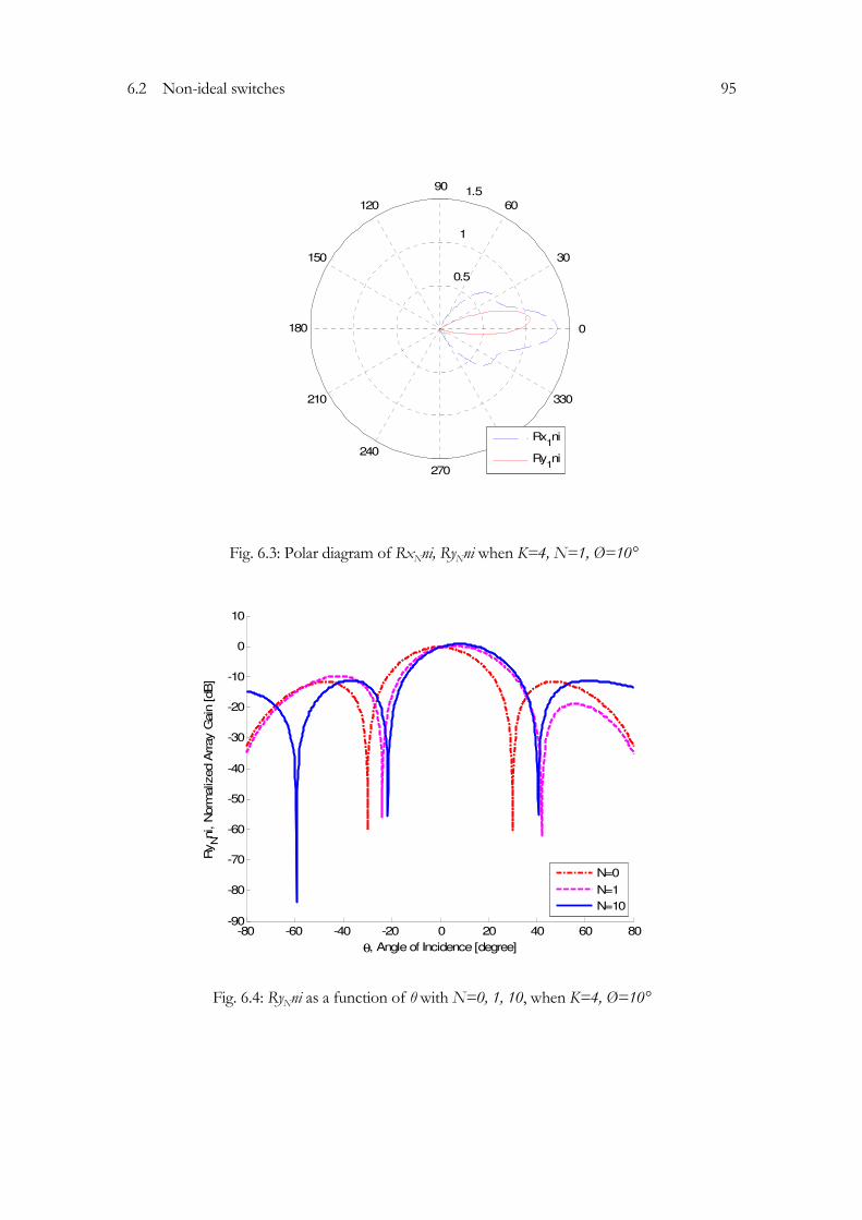
6.2 Non-ideal switches 95
Fig. 6.3: Polar diagram of RxNni, RyNni when K=4, N=1, Ø=10°
Fig. 6.4: RyNni as a function of θ with N=0, 1, 10, when K=4, Ø=10°
0.5
1
1.5
30
210
60
240
90
270
120
300
150
330
180 0
Rx1ni
Ry1ni
-80 -60 -40 -20 0 20 40 60 80-90
-80
-70
-60
-50
-40
-30
-20
-10
0
10
θ, Angle of Incidence [degree]
RyNni, N
orm
aliz
ed A
rray G
ain
[dB
]
N=0
N=1
N=10

96 Chapter 6. Multiplexing architecture, non-ideal behavior
Fig. 6.5 shows the angle deviation as a function of Ø with N=1, 2, 10, when K=4, α1=0dB, α2=25dB.
0 10 20 30 40 50 60 70 80 90-5
0
5
10
15
20
25
30
35
40
45
Φ, Expected viewing angle [degree]
∆Nni [d
egre
e]
N=1
N=2
N=10
Fig. 6.5: ∆Nni (in degree) as a function of Ø with N=1, 2, 10, when K=4, α1=0dB, α2=25dB
Comparing this with Fig. 6.1, we see that for all N, the angle deviation has become larger. Even with high filter bandwidth, the actual viewing angle still cannot perfectly follow the expected viewing angle. For K=4, within the range of 30°, ∆1_ni has a deviation range between (-0.2°, 4.4°). The angle deviation can be corrected in digital domain with a look-up table. However, the signal power loss hence also the modulated signal loss can give direct influence to BER. The re-quirement of the switch on/off difference can be discussed following the BER analysis.
6.3 Noise in a multiplexing system
In a multiplexing system, not only the signal but also the noise is pulse modulated. Noise from other frequencies can be mixed into the frequency of interest, as shown in Fig. 6.6.

6.3 Noise in a multiplexing system 97
Fig. 6.6: Noise folding when sampling
Assuming the noise spectrum is flat, and the noise RMS voltage is Vn,in, in a single channel, after mixing, the noise power in the frequency of interest can be separated into two parts: noise power from its own, Pnoise0, and noise power contributed from the n-th pairs of side frequencies, Pnoisen. Noise can be treated as signal without phase information. Based on equation (5.11), assume normalized resistor of 1Ω, the noise power can be expressed as
( )
( )
2
0 ,2
2
2
,
10
12 sin 1
n in
n n in
Pnoise K V nK
nPnoise K V n
n K
π
π
= ⋅ =
= ⋅ ⋅ ⋅ ≥
(6.7)
where n is the harmonic order number, and K is the number of antennas. Assuming a noise bandwidth BWnoise, and a signal bandwidth BWS, and the noise to signal bandwidth ratio as
noisen
S
BWR
BW= (6.8)
Note that fS=2*BWS. Defining Nr as the number of harmonic pairs that are contained within the noise bandwidth, we assume the number of harmonic pairs is an integer, instead of a decimal. One can write for Nr with integer function,
2
4
nr
RN INT
− =
(6.9)

98 Chapter 6. Multiplexing architecture, non-ideal behavior
The combined noise power of K paths can be directly summed over all channels. Taking noise summed up until the Nr-th side band
( ) ( )0
rN
r n
n
Pnsum K K Pnoise K=
= ⋅∑ (6.10)
The noise power gain Gnoiser(K) can be denoted as the summed noise power divided by the original noise power (within the signal bandwidth)
( )( )
,
2
1
1 12 sin
r
r
r
n in
N
n
Pnsum KGnoise K
V
nK
K n K
π
π=
=
= + ⋅ ⋅
∑
(6.11)
Fig. 6.7 shows the relation between Gnoiser(K) and the bandwidth ratio Rn, for K=4. It indicates that the smaller the ratio Rn, the better the noise reduction after multiplexing. When noise and signal use the same frequency band, the noise reduction is 6dB, which results in the same effect as in the conventional beam-forming.
Fig. 6.7: Relation of noise power gain Gnoiser(K) with bandwidth ratio Rn, when K=4

6.4 Frequency mixing 99
6.4 Frequency mixing
In chapter 4, we have explained the trade-off between antenna number K, signal bandwidth BW, and channel sampling frequency fS through equation (4.4). For a single channel, according to the Nyquist theory, the condition for no loss of data information is fS>2BW. However, this condi-tion is only valid when no interference comes from the adjacent channel. When the adjacent channel interference present, the signal and the interferer are both expanded in frequency at the multiplexer’s output, leading to an irrecoverable spectrum overlap, as shown in Fig. 6.8.
Fig. 6.8: Effect of adjacent channel interferer.
In order to prevent the spectrum overlap, the channel sampling frequency fS must be increased to make sure the spectrum expansion is not causing any overlap. As shown in Fig. 6.9, if fS>BWtotal, the interferer and signal spectrums are expended together, where BWtotal is the summed spectrum of signal, interferer, and the signal interferer frequency difference.
f
Interferer
Signal
fBWtotal fS
Fig. 6.9: Signal and interferer spectrum expansion without overlap.
For a K channel multiplexer, the switching frequency of the multiplexer fMUL needs to fulfill fMUL>K*BWtotal to make sure no overlap for each channel.

100 Chapter 6. Multiplexing architecture, non-ideal behavior
6.5 System simulations
Fig. 6.10 shows the system simulation diagram for multiplexing architecture in Advanced Design System (ADS). The goal for this test is to verify the spatial to frequency mapping theory that delivered in chapter 5. In this test, the desired and interference signal comes from 30° and -30°, respectively, and their carrier frequency is the same. The phase shifter in digital domain is pro-grammed at 30° to receive the desired signal. To simplify the simulation complexity, the follow settings are applied: RF carrier frequency is 26GHz, and sampling frequency for each channel is 50MHz.

6.5 System simulations 101
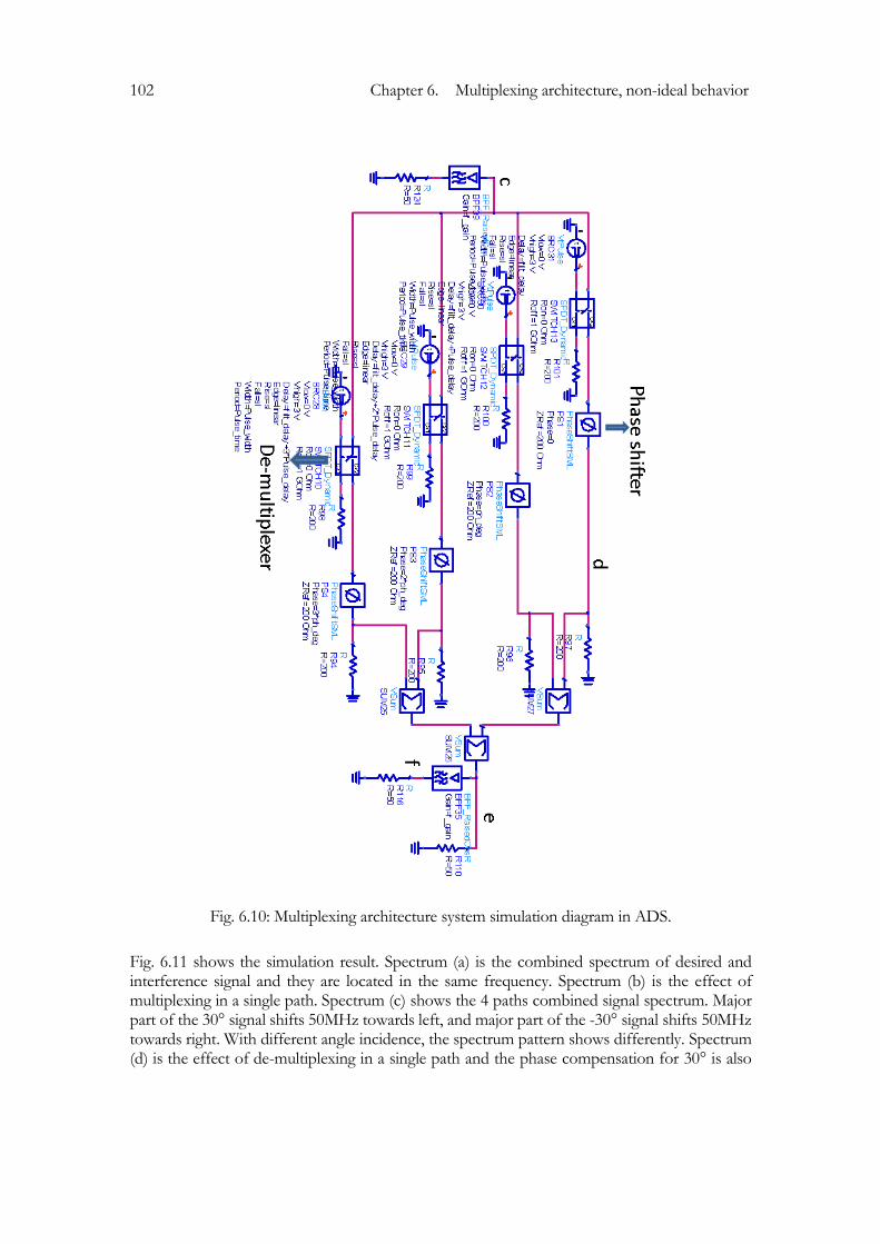
102 Chapter 6. Multiplexing architecture, non-ideal behavior
Fig. 6.10: Multiplexing architecture system simulation diagram in ADS.
Fig. 6.11 shows the simulation result. Spectrum (a) is the combined spectrum of desired and interference signal and they are located in the same frequency. Spectrum (b) is the effect of multiplexing in a single path. Spectrum (c) shows the 4 paths combined signal spectrum. Major part of the 30° signal shifts 50MHz towards left, and major part of the -30° signal shifts 50MHz towards right. With different angle incidence, the spectrum pattern shows differently. Spectrum (d) is the effect of de-multiplexing in a single path and the phase compensation for 30° is also

6.6 Power flow diagram for a multiplexed architecture 103
added. Spectrum (e) shows the 4 paths combined signal spectrum after phase shifter. Due to the phase compensation, the desired 30° signal shifts back to the original location, and the interfe-rence -30° signal spreads to other harmonic frequencies. Spectrum (f) is the final desired signal spectrum after a digital band-pass filter.
Fig. 6.11: Multiplexing architecture system simulation result in ADS. Spectrum (a)-(f) corres-ponding to point a-f in Fig. 6.8, respectively.
6.6 Power f low diagram for a multiplexed ar-chitecture
In chapter 3, we have introduced a signal, noise and distortion power (mW) flow diagram for analog phased-array, digital phased-array, and general case phased-array structure, respectively. For the multiplexing phased-array structure, we can also design a power flow diagram as shown in Fig. 6.12.

104 Chapter 6. Multiplexing architecture, non-ideal behavior
1 Lχ ⋅
totF
2
1FEF
χ⋅
2
1FE
Nχ
⋅
kT BW⋅
,tot inN
totN
FEN∆
3ADCIIP3FE
IIP
3tot
IIP
FEG
ADCN
ADCD
FED∆
totD
1
1FE
Gχ
⋅
FED
ADCI
ou tI
inI
inS
ADCS out
S
ADCF
Fig. 6.12: Signal, noise and distortion power flow diagram of a multiplexing phased-array
One can notice that except for parameters that has been explained previously, there are two extra parameters: χ1 and χ 2. They indicate the flexibility of the beam-forming system. The final array pattern is formed in digital domain. Hence the suppression factor L is located in the right part of the plane.
• χ1 represents the array coarse-pattern interference suppression, as in Fig. 5.7. It is varying between no coarse-pattern (χ1=1), and final-pattern (χ1=1/L).
• χ2 represents the array noise suppression, as in Fig. 6.7. It is varying between no noise suppression (χ2=1), and maximum noise suppression (χ2=K).
In brief, there are two types of power flow in Fig. 6.12,
• The flow of the interference signal, from Iin suppressed to IADC, thanks to the array coarse-pattern suppression. Then from IADC again suppressed to Iout due to the array fi-nal-pattern suppression.
• The flow of the desired signal, from Sin increased to SADC, due to the front-end gain, and then from SADC to Sout with a power gain of one.

6.7 Conclusion 105
6.7 Conclusion
In this chapter, we have discussed a few important non-idealities of a multiplexing phased-array architecture. To reduce the analog filter bandwidth, hence the ADC bandwidth, we have in-troduced an actual viewing angle to the expected viewing angle deviation. The smaller the band-pass filter bandwidth, the larger the angle deviation. This deviation can be compensated by creating a look-up table in the digital domain, but the power loss due to narrow band filtering is not correctable in digital domain. The channel isolation indicates the switching quality. If we don’t have a infinite channel isolation, even with high filter bandwidth, the actual viewing angle still can not perfectly follow the expected viewing angle. The channel isolation indicates the switching quality. If the channel isolation is not infinite, even with infinite filter bandwidth, the actual viewing angle still can not perfectly follow the expected viewing angle. To achieve the best signal to noise ratio improvement, the incoming noise bandwidth to signal bandwidth ratio should be small. If the signal and noise bandwidth are the same, then for a four antenna array, the SNR improvement is 6dB, which is the same improvement as the conventional beam-forming. For suitable applications, the power flow diagram can be used as a guideline to specify the block parameters. The system simulation result shows that a multiplexing phased-array architecture can achieve spatial to frequency mapping, and it is a good alternative for conventional phased-array architectures. Moreover, the simulation also shows that multiple sources (desired signal) selec-tion is possible with this architecture.

106 Chapter 6. Multiplexing architecture, non-ideal behavior

107
Chap t e r 7
7 Designs for the 30GHz compo-nents
In this chapter, the designs of the various components are reported, all for operation at 30GHz. The designs consist of LNA, multiplexer, mixer, clock generator, integrated delay line, and power amplifier. Section 7.1 explains the design requirements for the multiplexing phased-array architecture. Section 7.2 and 7.3 focus on LNA, multiplexer, and mixer design. Moreover, sub-system performance including these three components is reported. Section 7.4 is about the design of a clock generator which provides the switching signal. Section 7.5 discusses the delay line used to generate the front-end input phase difference in the integrated system in chapter 8. Section 7.6 describes the switching power amplifier design. Section 7.7 concludes this chapter.
7.1 Design requirements
The time multiplexing phased-array receiver uses a clock controlled multiplexer to combine K paths into one. The combined path contains the signals from the various paths in different time

108 Chapter 7. Designs for the 30GHz components
slots. After down-conversion, band-pass filtering, and digitization, the time multiplexed signal is de-multiplexed by the synchronous clock to recover the original K signals in the digital domain. Then, the signals are processed by beam-forming algorithms. As this system differs from a conventional receiver system, besides the front-end gain, noise, as well as non-linearity perfor-mance, there are a few more parameters which need to be considered carefully.
• The multiplexer essentially incorporates a switch for each path which loads the LNA and drives the mixer. To minimize the influence to the LNA and mixer when changing of the switch status, the input (S11) and output (S22) matching of the multiplexer should be maintained regardless of the switch status.
• In order to retain all amplitude and phase information from each antenna element up to the digital domain without mixing between each channel, the forward (S21) and reverse (S12) isolation of the multiplexer in an OFF (shut off) status should be designed to eliminate signals from other paths.
• To recover the signal from each path correctly in the digital domain, the sampling rate for each path (fS) must fulfill the Nyquist sampling theory: fS>2·BW, where BW is the sin-gle-sided bandwidth of the incoming modulated signal. As a result, the multiplexer sam-pling rate fMUL can be expressed as: fMUL= K·fS>2K·BW, which means that the incoming signal bandwidth is limited by the multiplexer switching speed.
• The technology used for the design is the 0.25µm SiGe BiCMOS process developed by NXP semiconductors [69]. It provides HBT NPN transistors with fT/fmax up to 130/140GHz, breakdown voltage of 2.0V, measured at VBE=0.65V, moderate CCB, Rpinch=3kΩ/sq, RE=2.5Ωum2, high transconductance, and competitive low pow-er-performance.
7.2 LNA and Multiplexer
7.2.1 Circuit design
Design LNA using SiGe technology has been widely studied [70-74]. The differential LNA (as shown in Fig. 7.1) consists of a inductively degenerated cascade Q1-Q2 and Q3-Q4, driving load inductors LC1-LC2. The cascaded LNA is necessary to reduce the miller effect and feedback caused by Cmu, in order to increase the power gain. Inductors LB1-LB2 and LE1-LE2 are selected together with the emitter width of Q1-Q2 in order to realize noise and impedance matching simultaneously.

7.2 LNA and Multiplexer 109
Emitter degeneration inductors LE1 and LE2 are used to to obtain Γin=Γ*opt, so that Γin and are Γopt conjugated matched. The high impedance of the current source generates a virtual ground for them. Scaling the input transistor Q1-Q2 (0.4um × 9.1um) brings the real part of the opti-mum source impedance for minimum noise figure close to 50Ω at 30GHz. The biasing voltage of Q1 and Q2 are 2.2V on the transistor base, in order to balance the output voltage swing and the remaining voltage headroom for the current source. Gyration of the emitter impedance of LE1-LE2 in series with the base resistance of Q1-Q2 sets the real part of the input impedance to 50Ω thereby matching Re[Zin] in the desired operation range. The inductor LB1-LB2 connected in series with the base is made series resonant with the input loop to set the imaginary part of the input impedance. Inductors LC1-LC2 are selected as matching components to tune the LNA output and the following multiplexer input at 30GHz.
Fig. 7.1: Simplified schematic of a 30GHz LNA
The circuit implementation of the multiplexer is shown in Fig. 7.2. It consists of parallel identical switches 1-4, with shared output load inductors LC3 & LC4. The switch uses current steering technique to minimize switching time. A differential common-emitter stage, formed by tran-sistor pair Q5-Q6, translates voltage into current. The switching function is achieved by tran-sistors Q7-Q10, where transistor pair Q8-Q9 provide the core amplification element of the switch. When control voltage CO1 is high, Q8 & Q9 are biased in forward active region, and Q7 & Q10 are in cut-off region, thus allowing the signal to pass from port 1 to 5. When CO1 is low, the bias current is steered toward transistors Q7 & Q10, which connects port 1 directly to the supply.

110 Chapter 7. Designs for the 30GHz components
Q7 Q8 Q10Q9CO1
VCC
CO2
VCC
Switch1
Switch2
Port2
CO3 Switch3
Port3
CO4 Switch4
Port4
A
B
Q6Q5
6mA
Port1
188pH 188pH
Vout
LC3 LC4
Q5-Q10: 6.0µm/0.4µm
Port5
Fig. 7.2: Simplified schematic of a 30GHz multiplexer
This topology inherently implements an absorptive switch. At input ports 1-4, it is ensured that the total current flow through the input transistors is always constant. At output port 5, the total current flow through the load inductors is also constant. Hence, the source and load impedance of the low noise amplifier and mixer will remain constant regardless of the state of the switch.

7.2 LNA and Multiplexer 111
Fig. 7.3: Die photo of the 30GHz LNA and multiplexer
Fig. 7.3 shows the integrated die photo of the 30GHz LNA and multiplexer. Note that RF input 2 is not power matched to the multiplexer. It is reserved for isolation measurement between each switch. The die area is 0.9mm2 and the active circuit occupies 0.2mm2.
7.2.2 Measurements
Fig. 7.4 shows the measurement setup for the 30GHz LNA and multiplexer die demonstrated in Fig. 7.3. The performance of the LNA-multiplexer combination is measured with switches of which the ON and OFF value can be varied with power supply 2 and 3.

112 Chapter 7. Designs for the 30GHz components
Fig. 7.4: Measurement setup of the 30GHz LNA and multiplexer
Fig. 7.5(a) and (b) show the S parameters of the circuit when the switch is in the ON/OFF state, respectively. S11 and S22 remain constant regardless of the switch status. The transmission, measured by S21 is 14.4dB in ON state and -9.3dB in OFF state, which gives 23dB of switch ON/OFF difference. Fig. 7.5(c) shows a comparison between simulated and measured noise figure. The minimum measured noise figure was 4.1dB at 30GHz. Fig. 7.5(d) is IIP3 measure-ment, and the input two tone frequencies are located at 29.950GHz and 30.050GHz, respec-tively. Hence the 3rd order intermodulation products are located at 29.850GHz and 30.150GHz, respectively. The measured IIP3 of the LNA multiplexer combination is -10dBm.
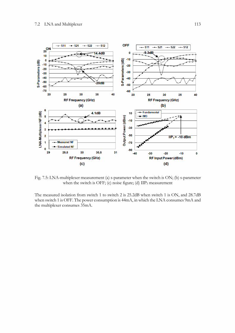
7.2 LNA and Multiplexer 113
Fig. 7.5: LNA-multiplexer measurement (a) s-parameter when the switch is ON; (b) s-parameter when the switch is OFF; (c) noise figure; (d) IIP3 measurement
The measured isolation from switch 1 to switch 2 is 25.2dB when switch 1 is ON, and 28.7dB when switch 1 is OFF. The power consumption is 44mA, in which the LNA consumes 9mA and the multiplexer consumes 35mA.

114 Chapter 7. Designs for the 30GHz components
7.3 LNA-multiplexer-mixer combination
7.3.1 Circuit design
The mixer design using SiGe technology has been presented extensively in the literatures [75-80]. The mixer design is a double-balanced Gilbert cell as shown in Fig. 7.6. It down-converts the RF signal at 30GHz to the IF frequency of 10GHz. Further down-conversion will be considered in a future design. The transconductance part of the mixer Q11-Q12 interfaces with the multiplexer output by inductors LC3 & LC4 in Fig. 7.2, and it is optimized to achieve the highest power gain and the lowest noise figure simultaneously. The bias current density and transistor size of the switching parts Q13-Q16 were chosen for the highest operating speed to maximize the con-version gain. The emitter degeneration resistors RE1-RE2 and the loading resistors RC1-RC2 are designed to trade-off the gain and the linearity performance of the mixer. The DC biasing for the input transistors Q11-Q12 is 1.7V, and the DC biasing for the output transistors Q13-Q16 is 2.7V.
Fig. 7.6: Simplified schematic of a 30GHz mixer

7.3 LNA-multiplexer-mixer combination 115
Fig 7.7 shows the simplified schematic which combines the LNA, the multiplexer, the mixer and the inter-connections between them.
Fig. 7.7: Simplified schematic of the 30GHz LNA, multiplexer, and mixer
Fig. 7.8 shows the integrated die photo of the above combined schematic. The die area is 0.9mm2 and the active circuit occupies 0.2mm2.
Fig. 7.8: Die photo of the 30GHz LNA, multiplexer, and mixer

116 Chapter 7. Designs for the 30GHz components
7.3.2 Measurements
Fig. 7.9 shows the measurement setup for the 30GHz LNA, multiplexer and mixer of the die that is demonstrated in Fig. 7.8. The performance of the LNA-multiplexer-mixer combination is measured with controllable switches implemented by power supply 2 and 3.
Fig. 7.9: Measurement setup of the 30GHz LNA, multiplexer, and mixer
The front-end measurement includes the LNA, the multiplexer, and the mixer with controllable switches. To evaluate the linearity of the front-end, the input third-order intercept point (IIP3) were measured. Fig. 7.10(a) shows the conversion gain of the front-end was measured with both ON/OFF switch situations as shown in. The RF frequency was swept from 21 to 39GHz with -33dBm input power. The measured maximum conversion gain is 18.9dB at 30GHz, and the switch ON/OFF difference is 23dB, corresponding with the isolation measurement result in the previous section. For the IIP3 measurement, two tones were applied to the RF input to generate IF signals at 9.950 and 10.050GHz. The third order intermodulation (IM3) products appear at 9.850 and 10.150GHz, respectively. The results are shown in Fig. 7.10(b). The measured IIP3 of the circuit is -22dBm. For input signal power of -45dBm, it is sufficient to operate in a linear region.

7.4 Clock generator 117
Fig. 7.10: LNA-multiplexer-mixer measurement (a) conversion gain with switch ON/OFF status (b) non-linearity IIP3.
7.4 Clock generator
7.4.1 Circuit design
The timing clock generator converts the input clock into four non-overlapping pulses, the control signals CO1-CO4, each with 25% duty cycle. The timing circuit is driven by a sinusoidal input clock but its operation is digital, divided in two parts: a modulus 4 counter and additional logic to obtain the four outputs. Table 7.1 represents the operation states of the timing circuit.
Q1 Q0 CO1 CO2 CO3 CO4
0 0 1 0 0 0
0 1 0 1 0 0
1 1 0 0 1 0
1 0 0 0 0 1
Table 7.1: Truth table operation of the timing circuit

118 Chapter 7. Designs for the 30GHz components
The modulus 4 counter is implemented as a two bit counter. The counting is done in gray mode instead of binary. In this way, only one bit changes at the transition between states. This is im-portant in high-frequency operation because it eliminates overlapping and glitches on CO1-CO4 that might occur when the outputs Q0 and Q1 have different switching speed. The circuit in-cluding the modulus 4 counters and additional logic is represented in Fig. 7.11.
Fig. 7.11: Timing clock generator circuit
The D-type flip-flops provide Q0 and Q1 outputs according to Table 7.1 (D1 = Q0 and D0 = Q1/). The outputs CO1-CO4 are obtained by combining the flip-flop outputs Q1 and Q0 using only NOR gates.
( )
( )
( )
( )
1 1/ 0/ 1 0 /
2 1/ 0 1 0 / /
3 1 0 1/ 0 / /
4 1 0/ 1/ 0 /
CO Q Q Q Q
CO Q Q Q Q
CO Q Q Q Q
CO Q Q Q Q
= ⋅ = +
= ⋅ = +
= ⋅ = +
= ⋅ = +
(7.1)
The flip-flop and NOR gates use differential emitter-coupled logic (ECL), to accommodate the differential control signals required to drive the four switching cells. The external clock input is also made differential. Fig. 7.12 shows the simulated waveforms of the outputs CO1-CO4 connected to the switching input of the switch cells.

7.4 Clock generator 119
0.0
-0.5
0.5
CO
1 [
V]
0.0
-0.5
0.5
CO
2 [
V]
0.0
-0.5
0.5C
O3
[V
]
0.0
-0.5
0.5
CO
4 [
V]
1.2 1.4 1.6 1.8 2.0 2.2 2.4 2.6 2.81.0 3.0
0.0
-0.4
0.4
Time [ns]
clk
[V]
Fig. 7.12: Simulated timing clock generator waveforms
The simulations were performed with a 4GHz input clock with differential 100Ω load. The peak to peak voltage swing on each output is larger than 600mV, which is adequate to drive the switch well into ON/OFF state.
Fig. 7.13: Die photo of the timing clock generator

120 Chapter 7. Designs for the 30GHz components
Fig. 7.13 shows the photograph of the timing clock generator. The clock input is at the left side while the other three sides are reserved for the three outputs CO1, CO3 and CO4. Output CO2 is internally matched to 100Ω (see Fig. 7.14) due to limited number of spaces for bond-pad placement. The outputs also include DC blocking capacitors for direct connection to the mea-surement setup. The die area is 0.8mm2 and the active circuit occupies 0.1mm2
7.4.2 Measurements
The output waveforms were measured with an Agilent MSO6104 oscilloscope. This oscilloscope has a bandwidth of 1GHz which limits the maximum measurement frequency, especially the rise time of the waveform (minimum of 0.35ns). Fig. 7.14 shows the measurement setup for the timing clock generator die shown in Fig. 7.13.
Fig. 7.14: Measurement setup of the timing clock generator
Fig. 7.15 shows the waveforms of the adjacent outputs CO3 and CO4 with an input clock of 600MHz. At the mean value of the waveforms (20mV) there is no overlapping. The rise time of the waveforms is close to 0.5ns which is mainly due to the oscilloscope. The operation range for this circuit is from 500MHz to 7GHz.

7.5 Input delay line 121
Fig. 7.15: Waveforms of the adjacent outputs CO3 and CO4.
7.5 Input delay line
7.5.1 Circuit design
In order to test the phased-array performance, we need to generate phase shifted input signals for the four channels. Due to measurement equipment limitations, the input phase shifts need to be generated on chip. Assuming a fixed incoming signal angle of 8.5°9, and adjacent antenna distance d=λ/2, according to (2.30), the corresponding electrical phase shift is 26.6°, and the corresponding time delay is 2.4p second. Fig 7.16 shows transmission line structures that can provide such a time delay.
9 The input angle is fixed to 8.5°. The reason is firstly due to the limited probe number (system implementation in chapter 8) and
chip area, and secondly, satellite communication requires viewing angle with in ±10°.

122 Chapter 7. Designs for the 30GHz components
Fig. 7.16: Transmission line structures for generating 26.6° electric phase shifting (a) 376um (b) 776um (c) 1176um (d) 1576um

7.5 Input delay line 123
The built-up of the transmission line is shown in Fig. 7.17.
Fig. 7.17: Transmission line structure (a) layout view. (b) cross-section view

124 Chapter 7. Designs for the 30GHz components
The distance between the transmission lines is 5um, and the single transmission line width is 5um. Table 7.2 shows the modeling parameters for the transmission lines shown in Fig. 7.16.
l c rS Z0 Loss ∆t φ
pH fF Ω Ω dB pS °
(a) 376u 244 25 4 99 0.18 2.4 26.7
(b) 776u 495 50 8.2 99 0.36 4.75 53.8
(c) 1176u 742 75 12.5 99.5 0.55 7.25 80.7
(d) 1576u 989 100 16.6 99.5 0.74 9.7 107.5
Table 7.2: Modeling parameters for the transmission lines
Because we do not want to introduce extra phase difference besides the intended ones that were shown in Fig. 7.16, the distances from each transmission line-end to the LNA input need to be equal for all channels. Structures in Fig. 7.18 have the same length, and they are used in the system level layout to connect the transmission line-end to the LNA input with equal distance.
Fig. 7.18: Transmission line structures for equal distance to LNA input (a) type 1 (b) type 2
The distance between the transmission lines is 6um, and the single transmission line width is 5um. Table 7.3 shows the modeling parameters for the transmission lines shown in Fig. 7.18.
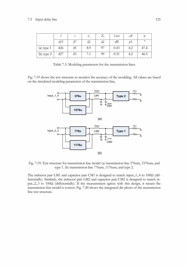
7.5 Input delay line 125
l c rS Z0 Loss ∆t φ
pH fF Ω Ω dB pS °
(a) type 1 426 45 8.9 97 0.43 4.2 47.4
(b) type 2 427 43 7.1 99 0.31 4.2 46.5
Table 7.3: Modeling parameters for the transmission lines
Fig. 7.19 shows the test structure to monitor the accuracy of the modeling. All values are based on the simulated modeling parameters of the transmission line,
Input_1_4
160pH
250fF
376u
1576u
Type 2
50Ω
Input_2_3
169pH
177fF
776u
1176u
Type 1
50Ω
(a)
(b)
LM1
LM2
CM1
CM2
Fig. 7.19: Test structure for transmission line model (a) transmission line 376um, 1576um, and type 1. (b) transmission line 776um, 1176um, and type 2.
The inductor pair LM1 and capacitor pair CM1 is designed to match input_1_4 to 100Ω (dif-ferentially). Similarly, the inductor pair LM2 and capacitor pair CM2 is designed to match in-put_2_3 to 100Ω (differentially). If the measurement agrees with this design, it means the transmission line model is correct. Fig. 7.20 shows the integrated die photo of the transmission line test structure.
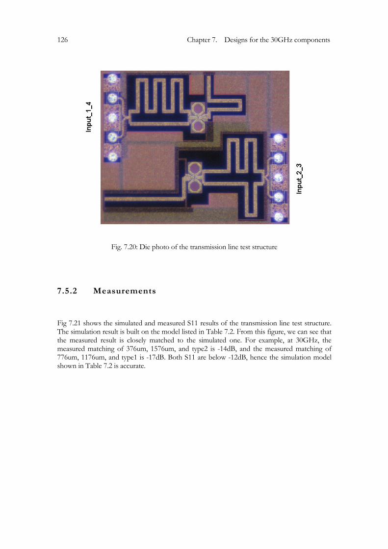
126 Chapter 7. Designs for the 30GHz components
Fig. 7.20: Die photo of the transmission line test structure
7.5.2 Measurements
Fig 7.21 shows the simulated and measured S11 results of the transmission line test structure. The simulation result is built on the model listed in Table 7.2. From this figure, we can see that the measured result is closely matched to the simulated one. For example, at 30GHz, the measured matching of 376um, 1576um, and type2 is -14dB, and the measured matching of 776um, 1176um, and type1 is -17dB. Both S11 are below -12dB, hence the simulation model shown in Table 7.2 is accurate.

7.6 Power amplifier 127
Fig. 7.21: Transmission line test structure: simulation result of S11 from (a) input_1_4. (b) in-put_2_3. And measurement result of S11 from (c) input_1_4. (d) input_2_3.
7.6 Power amplifier
As explained in chapter 1, although transmitter design is not the focus of this these, a switch controlled power amplifier is designed in this chapter for reference.
7.6.1 Circuit design
Design power amplifier using SiGe technology has been widely studied [81-87]. The simplified schematic of a 30GHz class A power amplifier with switch controls, is shown in Fig. 7.22. The input of the power amplifier connects to a 100Ω differential antenna, and the output matching

128 Chapter 7. Designs for the 30GHz components
network is designed through a large-signal load-line match to achieve large output power and high power efficiency.
Fig. 7.22: Simplified schematic of the 30GHz power amplifier with switch controls.
The PA switch control uses the same mechanism as used in the multiplexer design. When the control voltage ‘Switch_on’ is higher than ‘Switch_off’, Q4 & Q5 are biased in forward active region, and Q3 & Q6 are in cut-off region, thus allowing the signal to pass ‘Vin’ to ‘Vout’. When the control voltage ‘Switch_on’ is lower than ‘Switch_off’, the bias current is steered toward transistors Q3 & Q6, which connects ‘Vin’ directly to the supply. To achieve an optimal power gain per-formance, the emitter width of the bipolar transistor is chosen to be 20.7um and the DC current density is approximately 1mA per um-emitter-width. Together with the output matching resistor of 20Ω, in simulation, the power amplifier achieves an available gain of 16dB and maximum output power of +20dBm at 30GHz.

7.6 Power amplifier 129
Fig. 7.23: Die photo of the 30GHz power amplifier.
Fig. 7.23 shows the die photo of the 30GHz PA. The die area is 0.75mm2 and the active circuit occupies 0.2mm2.
7.6.2 Measurements
Fig. 7.24 shows the measurement setup for the 30GHz power amplifier. The performance of the PA is measured with switches that are controllable implemented by power supplies.

130 Chapter 7. Designs for the 30GHz components
Fig. 7.24: Measurement setup of the 30GHz power amplifier.
The measured spectrum with only DC biasing connected (without RF input signal) is shown in Fig. 7.25. The circuit is oscillating at frequency n*1.33GHz. It indicates that the PA bias loop is not stable.
Fig. 7.25: Measured PA output spectrum.

7.6 Power amplifier 131
7.6.3 Trouble shooting
To find the root cause of the PA instability, we first analyze the PA output stage. A separate PA output stage was available on die. It consists of input bondpads with transmission lines, PA output stage, and output bondpads with transmission lines, as shown in Fig. 7.26.
Fig. 7.26: Die photo of the power amplifier output stage verification circuit.
With load, open, and short de-embedding structures of the bondpads with transmission lines, we were able to characterize the loading resistance of the PA active stage as shown in Fig 7.27. The result shows that the output resistance is 25Ω. It is not exact 20Ω as expected, but the impact of this difference is small.

132 Chapter 7. Designs for the 30GHz components
freq (29.50GHz to 30.50GHz)
S(1
,1)
freq (29.50GHz to 30.50GHz)
S(1
,1)
Fig. 7.27: De-embedding PA output stage.
Next, we checked the bias loop with momentum simulations in the following steps10:
• Transistor core cells are removed and pins are reserved for multilevel simulation
• Matrices of vias are merged for simulation to reduce meshes
• Circular shapes are replaced with rectangles to reduce meshes
• Resistors, MIM caps, and diodes are removed to reduce meshes
• Only necessary metal layers and VIAs are reserved for DC biasing, signal flow and ground plane. We made sure that removing other layers will not influence the circuit function.
• Removed elements are added to the schematic simulation
The simplified layout for momentum simulation is shown in Fig. 7.28. The simulation schematic with Momentum cell and re-adding removed cells is shown in Fig. 7.29.
10 Thanks to my colleague Yu Pei who helped to perform this simulation

7.6 Power amplifier 133
Fig. 7.28: Simplified layout for full EM (electromagnetic) momentum simulation.
Fig. 7.29: Simulation schematic with momentum cell and re-adding removed cells.

134 Chapter 7. Designs for the 30GHz components
The small signal simulation results of the above schematic are shown in Fig 7.30.
Fig. 7.30: Small signal simulation results of the re-modeled PA (a) K factor (b) B1f factor
The results show that through the displayed frequency segment, the K factor drops below 1 and the B1f factor drops below 0. It indicates that the PA is not unconditionally stable, and the reason is the non-optimized layout design by adding small base resistors (10Ω) to transistor Q1 to Q6 in Fig. 7.22, we can improve the PA stability as shown in Fig. 7.31.
Fig. 7.31: Small signal simulation results of the re-modeled PA, adding small base resistors (a) K factor (b) B1f factor
The results show that through the displayed frequency segment, the K factor stays above 1 and the B1f factor stays above 0. It indicates that the PA is unconditionally stable. In conclusion, for such a high power level circuit, only the EM simulation on the signal path is not sufficient. It is necessary to perform the EM simulation also including the biasing lines.

7.7 Conclusion 135
7.7 Conclusion
In this chapter, the various designs of 30GHz components have been discussed. It comprises the LNA, the multiplexer, the mixer, the clock generator, the integrated delay lines, and the power amplifier. The measurement of the PA shows unstable behavior, and the root cause was found to be the non-optimized layout design. Simulation result shows that by adding small base resistors to the PA transistors, the un-stable problem can be avoided. The components will be connected to construct a time multiplexed phased-array receiver system in chapter 8.

136 Chapter 7. Designs for the 30GHz components

137
Chap t e r 8
8 System integration and verifica-tion
After demonstrating the 30GHz components in the previous chapter, a fully integrated 30GHz time multiplexed phased-array receiver in SiGe technology is introduced in this chapter. Section 8.1 introduces a first integration of the system, in which only one channel is activated. Section 8.2 demonstrates an integrated system with four channels. The delay line explained from chapter 7.5 is used to generate fixed electronic phase shift of 26.6° which is equivalent to a spatially angle of 8.5°. Section 8.3 makes conclusions for this chapter.
8.1 System with one channel
The time multiplexed phased-array receiver system with one activated channel includes one LNA, the multiplexer, the mixer, and the clock generator. Note that the other three channels are internally terminated by 100Ω resistors. The measurement setup of the system is shown in Fig. 8.1. The die photo of the fabricated circuit is shown in Fig. 8.2.
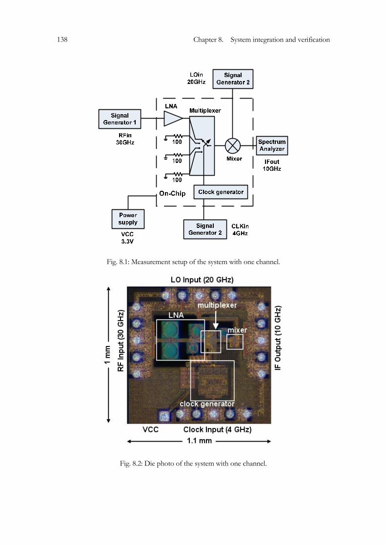
138 Chapter 8. System integration and verification
Fig. 8.1: Measurement setup of the system with one channel.
Fig. 8.2: Die photo of the system with one channel.

8.1 System with one channel 139
Fig. 8.3 shows the input matching for the system with one channel activated. At 30GHz, S11 is -30dB.
Fig. 8.3: Input matching for the system with one channel activated.
Fig. 8.4 shows the output spectrum of the mixer with a -38dBm RF signal input at 30GHz, -5dBm LO signal at 20GHz, and -10dBm clock signal at 4GHz (1GHz clock for each channel). The output behaves as a switched 10GHz tone with 1GHz sampling spacing and 25% du-ty-cycle, confirmed by the theory shown in Fig. 5.2.
Fig. 8.4: Measured one channel system output spectrum at IF, spectrum view (a) zoom in (b) zoom out. The output behaves as a switched 10GHz tone with 1GHz sampling spacing and 25%
duty-cycle.

140 Chapter 8. System integration and verification
Compared to a conventional receiver, the multiplexer with 25% duty cycle receives 1/4 of the input signal power, which gives another 12dB drop for the 0th order harmonic at 10GHz (this drop will be compensated in the digital domain by combining 4 paths together). Considering also the 3dB loss in each cable, 4.7dB loss in each balun-probe setting and the conversion gain of 18.9dB, the output power at 10GHz can be calculated as
( 2)
38 3 4.7 18.9 12 4.7 6 49.5cableloss cablelossinput power balunloss F E gain samplingloss balunloss
dBm dB dB dB dB dB dB dBm×−
− − − + − − − = − (8.1)
Resulting in -49.5dBm, which closely agrees to the value shown in marker 1 (Fig. 8.4(a)).
8.2 System with four channels
With the successful design of the system with one channel and the demonstrated delay lines introduced in chapter 7.5, we can demonstrate the time multiplexed phased-array receiver system with four activated channels. The demonstrated system includes the delay lines, the LNA, the multiplexer, the mixer, and the clock generator.

8.2 System with four channels 141
8.2.1 Demonstration with one input signal
The system measurement includes the delay lines, the LNA, the multiplexer, the mixer, and the clock generator. The measurement setup is shown in Fig. 8.5. The delay line explained from chapter 7.5 is used to generate fixed electronic phase shift of 26.6° which is equivalent to a spatial angle of 8.5°.
Fig. 8.5: Measurement setup of system with four channels, incoming signal angle of 8.5°.

142 Chapter 8. System integration and verification
Fig. 8.6: Die photo of the system with four channels, incoming signal angle of 8.5°.
The die photo of the fabricated circuit is shown in Fig. 8.6. Note that the delay lines 376um, 776um, 1176um, and 1576um are used to make time delay, and the delay lines type 1 and type 2 are used to connect the line-ends with the LNA input with equal line distance.

8.2 System with four channels 143
Fig. 8.7: Input matching for system with four channels, incoming signal angle of 8.5°.
Fig. 8.7 shows the input matching of the system with four channels, including the delay lines. At 30GHz, S11 is -21dB.

144 Chapter 8. System integration and verification
Fig. 8.8: Four channels system output spectrums at IF, incoming signal angle of 8.5° (a) theo-retical (b) simulated (c) measured, zoom in (d) measured, zoom out
Fig. 8.8 shows the four channels system output spectrums at the mixer output with incoming signal angle of 8.5°. Fig. 8.8(a) is the theoretical normalized spectrum assuming ideal block components. Fig. 8.8(b) is the simulated spectrum in Cadence with all blocks implemented in practice. Fig. 8.8(c) and (d) are the measured spectrums. The theoretical, simulated, and meas-ured spectrums show good agreement with each other. This confirms the theory explained in chapter 5: the time multiplexed phased-array architecture can achieve spatial domain to fre-quency domain mapping. Moreover, with 8.5º spatial input, the major part of the energy is stored in the fundamental and ±1 harmonics. So in this case, an analog band-pass filter with a single sideband bandwidth larger than 1GHz can successfully receive this signal.

8.2 System with four channels 145
8.2.2 Demonstration with two input signals
With a little change in the delay lines connections, we can make the system demonstrate two signal inputs. One signal comes from a spatial angle of 8.5°, and the other signal comes from a spatial angle of -8.5°. The measurement setup is shown in Fig. 8.9. The spatial angle of 8.5° is generated from the following way of connections:
• The 376um delay line is connected to the LNA 1 that opens at first.
• The 776um delay line is connected to the LNA 2 that opens at second.
• The 1176um delay line is connected to the LNA 3 that opens at third.
• The 1576um delay line is connected to the LNA 4 that opens at fourth.
The spatial angle of -8.5° is generated in the above way but with the opposite sequence:
• The 376um delay line is connected to the LNA 4 that opens at first.
• The 776um delay line is connected to the LNA 3 that opens at second.
• The 1176um delay line is connected to the LNA 2 that opens at third.
• The 1576um delay line is connected to the LNA 1 that opens at fourth.
So connecting the 376um and 1576um delay lines to LNA 1 and LNA 4 at the same time; and connecting 776um and 1176um delay lines to LNA 2 and LNA 3 at the same time, we can generate two input signals from angle 8.5° and -8.5º.
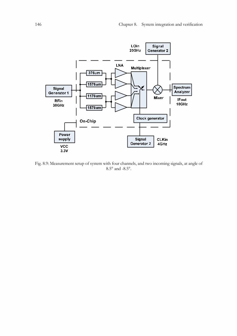
146 Chapter 8. System integration and verification
Fig. 8.9: Measurement setup of system with four channels, and two incoming signals, at angle of 8.5° and -8.5°.

8.2 System with four channels 147
Fig. 8.10: Die photo of the system with four channels, and two incoming signals, at angle of 8.5° and -8.5°.
The die photo of the fabricated circuit is shown in Fig. 8.10. Note that the delay lines 376um, 776um, 1176um, and 1576um are used to make time delay, and the delay lines type 1 and type 2 are used to connect line ends with LNA input with equal distance.

148 Chapter 8. System integration and verification
Fig. 8.11: Input matching for system with four channels, two incoming signals angle of 8.5° and -8.5°.
Fig. 8.11 shows the input matching of the system with four channels, including the delay lines. At 30GHz, S11 is -20dB.

8.3 Conclusion 149
Fig. 8.12: Four channels system output spectrums at IF, two incoming signals angle of 8.5° and -8.5° (a) theoretical (b) simulated (c) measured, zoom in (d) measured, zoom out
Fig. 8.12 shows the four channels system output spectrums at the mixer output with two in-coming signals, at angle of 8.5° and -8.5°. Fig. 8.12(a) is the theoretical normalized spectrum assuming ideal block components. Fig. 8.12(b) is the simulated spectrum in Cadence with all blocks implemented in practice. Fig. 8.12(c) and (d) are the measured spectrums. Also, with 8.5º and -8.5º spatial inputs, the major part of the energy is stored in the fundamental and ±1 har-monics. We can not separate these two input signals by the coarse filtering, because they are symmetrical in space, and will give the same response. However, with final spatial filtering in the digital domain, they can be separated. The simulated and measured spectrums have un-equal +1 and -1 harmonic amplitude, while the ideal theoretical spectrum has equal +1 and -1 harmonics amplitude. This is due to the non-ideal delay lines and multiplexing switches. Comparing with Fig. 8.8, the frequency spectrum pattern has changed due to incoming signal differences. This confirms with the theory explained in chapter 5.

150 Chapter 8. System integration and verification
8.3 Conclusion
In this chapter, we give three demonstrations of the time multiplexed phased-array receiver. A system with one activated channel proves that the block components designed in chapter 7 can be used to construct a working time multiplexing system. A system with four activated channels is demonstrated with two scenarios: one with single fixed input signal from a spatial angle of 8.5°, and the other with two fixed input signals from spatial angles of 8.5º and -8.5º. These demon-strations confirm the theory explained in chapter 5: the time multiplexed phased-array archi-tecture can achieve spatial domain to frequency domain mapping. Moreover, with small angle of incidence (8.5º), the frequency spectrum energy is focused on a few major harmonics (funda-mental, +1 and -1 harmonics). The core size of the 4 channel system without area optimization is 1mm by 1.2mm, which is relatively small compare with conventional 4-channel phased-array systems.

151
Chap t e r 9
9 Conclusions and future works
9.1 Conclusion
This thesis provides a system approach analysis method for phased-array receivers. A single path receiver optimization method was studied first. A design flow for trade-off between RF front-end and ADC block performance by translating ADC parameters into RF domain is in-troduced. This approach indicates two variables, ∆NFE and ∆DFE, for achieving optimum dy-namic range in a receiver chain. Associating these variables to the power consumption enables the trade-off between RF and ADC block for minimum overall power consumption. After that, two types of multi-path receiver, namely, analog beam-forming and digital beam-forming are analyzed as a single chain receiver with their equivalent model. It started with analyzing the difference between phased-array and single-chain receivers from noise and linearity perspectives and the result indicates that for both cases, the total noise figures are reduced due to non-correlated noise adding, and the total IIP3 are increased due to interference cancellation. At last, this chapter provided a general case of beam-forming analysis, and two parameters β1 and β2 are introduced to indicate the flexibility of the beam-forming. When K<β1< K2 and 1<β2<K, the

152 Chapter 9. Conclusions and future works
system is partly analog, and partly digital beam-forming. On system design level, β1 and β2 can be used as another design dimension to perform system optimization with various applications.
Two-step beam-forming using space-frequency transformation in a time-multiplexed phased-array receiver has been introduced. This architecture can achieve spatial domain to frequency domain mapping, and two steps of spatial filtering, namely coarse and final spatial filtering. These properties enable the possibility of phased-array analog and digital co-design, and generalized phased-array system design. Specifically, we have discussed the multiplexing archi-tecture from a mathematical point of view. We used various models to understand the properties of the system. Firstly, the properties of the analog combined signal were described and a simi-larity with traditional phase modulation theory was explained. Secondly, a new coefficient function Dn was introduced to help understand the properties of the combined signal. Thirdly, we introduced a new concept: spatial to frequency transformation. Next, by processing the signals in the digital domain, the final array pattern was introduced. Furthermore, the array pattern was compared with the traditional analog beam-forming array pattern and key system parameters have been revealed.
Furthermore, we have discussed a few important non-idealities of a multiplexing phased-array architecture. To reduce the analog filter bandwidth, hence the ADC bandwidth, we have in-troduced an actual viewing angle to the expected viewing angle deviation. The smaller the band-pass filter bandwidth, the larger the angle deviation. This deviation can be compensated by creating a look-up table in the digital domain, but the power loss due to narrow band filtering is not correctable in digital domain. The channel isolation indicates the switching quality. If we don’t have a infinite channel isolation, even with high filter bandwidth, the actual viewing angle still can not perfectly follow the expected viewing angle. The channel isolation indicates the switching quality. If the channel isolation is not infinite, even with infinite filter bandwidth, the actual viewing angle still can not perfectly follow the expected viewing angle. To achieve the best signal to noise ratio improvement, the incoming noise bandwidth to signal bandwidth ratio should be small. If the signal and noise bandwidth are the same, then for a four antenna array, the SNR improvement is 6dB, which is the same improvement as the conventional beam-forming. For suitable applications, the power flow diagram can be used as a guideline to specify the block parameters. The system simulation result shows that a multiplexing phased-array architecture can achieve spatial to frequency mapping, and it is a good alternative for conventional phased-array architectures. Moreover, the simulation also shows that multiple sources (desired signal) selec-tion is possible with this architecture.
At circuit level, the various designs of 30GHz components have been discussed. It comprises the LNA, the multiplexer, the mixer, the clock generator, the integrated delay lines, and the power amplifier. The measurement of the PA shows unstable behavior, and the root cause was found to be the non-optimized layout design. Simulation shows that by adding small base resistors to the PA transistors, the instability problem can be avoided. Furthermore, we have given three demonstrations of the time multiplexed phased-array receiver. A system with one activated channel proves that the block components previously designed can be used to construct a working time multiplexing system. A system with four activated channels has been demonstrated with two scenarios: one with single fixed input signal from a spatial angle of 8.5°, and the other with two fixed input signals from spatial angles of 8.5º and -8.5º. These demonstrations confirm

9.2 Future works 153
the theory explained previously: the time multiplexed phased-array architecture can achieve spatial domain to frequency domain mapping. Moreover, with small angle of incidence (8.5º), the frequency spectrum energy is focused on a few major harmonics (the fundamental, and the +1 and -1 harmonics). The core size of the 4 channel system without area optimization is 1mm by 1.2mm, which is relatively small compare with conventional 4-channel phased-array systems.
This architecture is suitable for applications with limited viewing angle. With a band-pass filter at IF in front of the ADC in the analog domain, the suppressed interference in both frequency and spatial domain can relax the ADC design complexity. Meanwhile, the preserved phase infor-mation is processed in digital domain for final array patterning and multiple source selection (if applicable).
9.2 Future works
For future works, following aspects could be added:
• The study of other methods which can provide weighting functions for the array channels, such as programmable switches, programmable band-pass filters, etc.
• The study of the modulated signal impact, including the BER, EVM and SNR degrada-tion, due to the energy loss during the analog band-pass filtering process.
• The study of the non-ideal switching behavior due to timing jitter, phase noise and isola-tion between switches (self mixing).
• The complete system demonstration including the digital signal processing design.
• The phased-array transmitter implementation based on the two step beam-forming time multiplexed architecture.

154 Chapter 9. Conclusions and future works

155
Chap t e r 10
10 Original contributions
The original contributions of the work presented in this thesis are listed below:
• This thesis provides a mapping method that translates ADC noise and linearity parameters into the RF domain.
• This thesis introduces two parameters ∆NFE , ∆DFE for system optimization including both RF front-end and ADC.
• This thesis introduces analog beam-forming and digital beam-forming equivalent Friis Noise (F) and linearity (IIP3) equation.
• This thesis provides a generalized phased-array receiver simulation that enables analog and digital co-design: two-steps beam-forming using space-frequency transformation in a time-multiplexed phased-array receiver.
• This thesis initiates space to frequency mapping theory by introducing coefficient Dn.

156 Chapter 10. Original contributions
• This thesis provides mathematical analysis method for time-multiplexed phased-array architecture, including ideal and non-ideal situation.
• This thesis provides a time-multiplexing phased-array architecture power flow diagram including both RF and ADC.
• This thesis implements a 30GHz 4 channel multiplexer in SiGe technology.
• This thesis implements a 30GHz 4-channel time-multiplexing phased-array front-end system SiGe technology.
157
References
[1] G. E. Moore, "Cramming more components onto integrated circuits," Electronics, vol. 38, no. 8, April. 1965.
[2] IEEE Std 802.15.1-2005 - Part 15.1: Wireless medium access control (MAC) and Physical layer (PHY) specifications for wireless personal area networks (WPANs).
[3] S. Cherry, "Edholm's law of bandwidth," IEEE Spectrum, vol. 41, no. 7, pp. 58-60, July 2004.
[4] C. E. Shannon, "Communication in the presence of noise," Proceedings of the IEEE, vol. 72, no. 9, pp. 1192-1201, Sept. 1984.
[5] A. M. Niknejad et al., mm-Wave Silicon Technology: 60GHz and beyond, Springer, 2008.
[6] "IEEE 802.16 Standard for Local and Metropolitan Area Networks Part 16: Air Inter-face for Fixed Broadband Wireless Access Systems", 2004.
[7] R. Ludwig, et al., RF Circuit Design, Theory and Applications, Prentice Hall NJ, 2000.
[8] S. A. Townes et al., “Operational demonstration of Ka-band Telecommunications for the Mars Reconnaissance Orbiter,” IEEE Aerospace Conference, March 2003.
[9] B. C. Kane et al., "Smart Phased Array SoCs: A Novel Application for Advanced SiGe HBT BiCMOS Technology" Proceedings of the IEEE, vol. 93, no. 9, pp. 1656-1668, Sept. 2005.
[10] Y. Yu et al., "A 60GHz Phase Shifter Integrated With LNA and PA in 65nm CMOS for Phased Array Systems," IEEE Journal of Solid-State Circuits, vol. 45, no. 9, pp. 1697-1709, Sep. 2010.
[11] J. Paramesh et al., "A Four-Antenna Receiver in 90-nm CMOS for Beamforming and Spatial Diversity," IEEE Journal of Solid-State Circuits, vol. 40, no. 12, pp. 2515-2524, Dec. 2002.

158 References
[12] A. Natarajan et al., "A Bidirectional RF-Combining 60GHz Phased-Array Front-End," IEEE international Solid-State Conf. (ISSCC), 2010, pp. 40-41.
[13] K. Koh et al., "An X- and Ku-Band 8-Element Phased-Array Receiver in 0.18um SiGe BiCMOS Technology," IEEE Journal of Solid-State Circuits, vol. 43, no. 6, pp. 1360-1371, Jun. 2008.
[14] K. Koh et al., "A Millimeter-Wave (40-45GHz) 16-Element Phased-Array Transmitter in 0.18-um SiGe BiCMOS Technology," IEEE Journal of Solid-State Circuits, vol. 44, no. 5, pp. 1498-1509, May. 2009.
[15] A. Valdes-Garcia et al., "A SiGe BiCMOS 16-Element Phased-Array Transmitter for 60GHz Communications," IEEE international Solid-State Conf. (ISSCC), 2010, pp. 218-219.
[16] P. Baltus et al., "A 3.5mW 2.5GHz diversity receiver in Silicon-On-Anything," IEEE Journal of Solid-State Circuits, vol. 33, no. 12, pp. 2074-2079, Dec. 1998.
[17] P. Baltus et al., "Optimizing RF Front Ends for Low Power," Proceedings of the IEEE, Dec. 2000.
[18] S. Kishimoto et al., "A 60-GHz Band CMOS Phased Array Transmitter utilizing Compact Baseband Phase Shifters," in IEEE Radio Frequency Integrated Circuits Symposium, 2009.
[19] K. Raczkowski et al., "A Wideband Beamformer for a Phased-Array 60GHz Receiver in 40nm Digital CMOS," IEEE international Solid-State Conf. (ISSCC), 2010, pp. 40-41.
[20] A. Natarajan et al., "A 77-GHz Phased-Array Transmitter With On-Chip Antennas in Silicon: Transmitter and Local LO-Path Phase Shifting," IEEE Journal of Solid-State Cir-cuits, vol. 41, no. 8, pp. 2807-2819, Dec. 2006.
[21] K. Scheir et al., "A 52GHz Phased-Array Receiver Front-end in 90nm Digital CMOS," IEEE international Solid-State Conf. (ISSCC), 2008.
[22] Wei L. Chan et al., "A 60GHz-Band 2×2 Phased-Array Transmitter in 65nm CMOS," IEEE international Solid-State Conf. (ISSCC), 2010, pp. 42-43.
[23] A. Behzad et al., "A fully integrated MIMO multiband direct conversion CMOS tran-seiver for WLAN applications (802.11n)," IEEE Journal of Solid-State Circuits, vol. 42, no. 12, pp. 2795-2808, Dec. 2007.
[24] Y. Palaskas et al., "A 5-GHz 108-Mb/s 2×2 MIMO transeiver RFIC with fully integrated 20.5-dBm P1dB power amplifier in 90-nm CMOS," IEEE Journal of Solid-State Circuits, vol. 41, no. 12, pp. 2746-2756, Dec. 2006.

References 159
[25] O. Degani et al., "A 1×2 MIMO multi-band CMOS transceiver with an integrated front-end in 90nm CMOS for 802.11a/g/n WLAN applications," IEEE ISSCC Dig. Tech. Papers, Feb. 2008, pp. 356-357.
[26] L. Nathawad et al., "A dual-band CMOS MIMO radio SoC for IEEE 802.11 wireless LAN," IEEE ISSCC Dig. Tech. Papers, Feb. 2008, pp. 358-359.
[27] L. Khuon et al., "An area-efficient 5-GHz multiple receiver RFIC for MIMO WLAN applications," IEEE RFIC Symp. Dig., Jun. 2006, pp. 11-13.
[28] S. Farzaneh et al., "A Novel Amplitude-Phase Weighting for Analog Microwave Beamforming," IEEE Transactions on antennas and propagation, vol. 54, no. 7, pp. 1997-2008, July. 2006.
[29] F. Tzeng et al., "A CMOS Code-Modulated Path-Sharing Multi-Antenna Receiver Front-End," IEEE Journal of Solid-State Circuits, vol. 44, no. 5, pp. 1321-1335, May. 2009.
[30] J. D. Fredrick et al., "A Smart Antenna Receiver Array Using a Single RF Channel and Digital Beamforming," IEEE Transactions on microwave theory and techniques, vol. 50, no. 12, pp. 3052-3058, Dec. 2002.
[31] J. Rogers et al., Radio Frequency Integrated Circuit Design, Artech House, 2003.
[32] H. T. Friis, "Noise figure of radio receiver," Proceedings of the IRE, vol. 32, no. 7, pp. 419-422, July. 1944.
[33] D. M. Pozar. Microwave Engineering, John Wiley and Sons, Inc., 2nd edition, 1998.
[34] K. McClaning et al., Radio Receiver Design, Noble Publishing Corp., 2000.
[35] B. Razavi, RF Microelectronics, Prentice Hall, 1998.
[36] C. Toumazou et al., Trade-offs in Analog Circuit Design, Kluwer Academic, 2002.
[37] G. Fetweis, "Introduction to Communications," Lectures script, 2002.
[38] F. Bowman, Introduction to Bessel Functions, Dover, 1958.
[39] L. W. Couch II, Digital and Analog Communication Systems: 7the Edition, Prentice Hall, 2006.
[40] D. Parker et al., "Phased Arrays - Part I: Theory and Architectures," IEEE Transactions on Microwave Theory and Techniques, vol. 50, no. 3, pp. 678-687, March 2002.
[41] M. Skolnik, Radar Systems, 3rd ed. New York: McGraw-Hill, 2001.
[42] G. E. Moore, "Cramming more components onto integrated circuits," Electronics, vol 38, no. 8, pp. 114-117, April. 1965.

160 References
[43] T. Yamaji et al., "A Four-Input Beam-Forming Downconverter for Adaptive Antennas," IEEE Journal of Solid-State Circuits, vol. 38, no. 10, pp. 1619-1625, Oct. 2003.
[44] D. Parkerd et al., "Phased Arrays - Part II: Implementations, Applications, and Future Trends," IEEE Transactions on Microwave Theory and Techniques, vol. 50, no. 3, pp. 688-698, March 2002.
[45] A. Natarajan et al., "A Fully Integrated 24-GHz Phased-Array Transmitter in CMOS," IEEE Journal of Solid-State Circuits, vol. 40, no. 12, pp. 2502-2514, Dec. 2005.
[46] H. Hashemi et al., "A 24-GHz SiGe Phased-Array Receiver - LO Phase-Shifting Ap-proach," IEEE Transactions on Microwave Theory and Techniques, vol. 53, no. 2, pp. 614-625, Feb. 2005.
[47] R. Tayrani et al., "Broadband SiGe MMICs for phased array radar applications," IEEE Journal of Solid-State Circuits, vol. 38, no. 9, pp. 1462-1470, Sep. 2003.
[48] R.J. Mailloux, Phased-array antenna handbook, 2nd ed. Artech point on Demand, 2005.
[49] B. Razavi, "CMOS RF Receiver Design for Wireless LAN Applications," IEEE Radio and Wireless Conf., pp. 275-280, Aug. 1999.
[50] T. Burger et al., "A 13.5-mW 185-Msample/s ∆Σ modulator for UMTS/GSM dual-standard IF reception," IEEE Journal of Solid-State Circuits, vol. 36, no. 12, pp. 1868-1878, Dec. 2001.
[51] A. Rofougaran et al., "A single-chip 900-MHz spread-spectrum wireless tranceiver in 1-um CMOS. II. Receiver design," IEEE Journal of Solid-State Circuits, vol. 33, no. 4, pp. 535-547, Apr. 1998.
[52] J. Rudell et al., "Recent developments in high integration multi-standard CMOS tran-sceivers for personal communication systems," Proc. Int. Symp. Low Power Electronics and Design, pp. 149-154, Aug. 1998.
[53] D. Shaeffer et al., "A 11-mW, 0.5-um CMOS GPS receiver with wide dynamic-range active filters," IEEE Journal of Solid-State Circuits, vol. 33, no. 12, pp. 2219-2231, Dec. 1998.
[54] K. Lee et al., "Full-CMOS 2GHz WCDMA direct conversion transmitter and receiver," IEEE Journal of Solid-State Circuits, vol. 38, no. 1, pp. 43-53, Jan. 2003.
[55] A. R. Behzad et al., "A 5-GHz direct-conversion CMOS transceiver utilizing automatic frequency control for the IEEE802.11a wireless LAN standard," IEEE Journal of Sol-id-State Circuits, vol. 38, no. 12, pp. 2209-2220, Dec. 2003.
[56] A. Emira et al., "A low-power CMOS complex filter with frequency tuning," IEEE Trans. Circuit Syst. II, Analog Digit. Signal Process., vol. 50, no. 10, pp. 742-754, Oct. 2003.

References 161
[57] A. A. Abidi, "Direct-conversion radio transceivers for digital communications," IEEE Journal of Solid-State Circuits, vol. 30, no. 12, pp. 1399-1410, Dec. 1995.
[58] M. Yuce et al., "SOI CMOS Implementation of a Multirate PSK Demodulator for Space Communications," IEEE Trans. Circuit Syst., vol. 54, no. 2, pp. 420-431, Feb. 2007.
[59] G. Gonzalez, Microwave Transistor Amplifiers Analysis and Design, Upper Saddle River, NJ: Prentice Hall, 1997.
[60] P. Baltus, "Minimum Power Design of RF Front Ends," Ph.D. dissertation, Eindhoven University of Technology, 2004.
[61] R. van de Plassche, CMOS Integrated Analog-to-Digital and Digital-to-Analog Converters. Kluwer Academic Publishers, 2003.
[62] J. Crols et al., CMOS Wireless Transceiver Design, Kluwer, Jun. 1997.
[63] W. Sheng et al., "CMOS RF Receiver System Design: A Systematic Approach," IEEE Transaction on Circuit and System, vol. 53, no. 5, pp. 1023-1034, May. 2006.
[64] C. E. Shannon, "Communication in the presence of noise," Proc. Institute of Radio Engineers, vol. 37, no. 1, pp. 10-21, Jan. 1949.
[65] A. V. Oppenheim et al., Signal and Systems: second edition, Prentice Hall, Dec. 1999.
[66] A. B. Carlson et al., Communication Systems: 3rd edition, McGraw Hill, 1986.
[67] J. D. Gibson, The Communication Handbook, CRC Press, 1997.
[68] A. Biswas, "Novel brick-wall filters based on the auditory system," IEEE International Conference on Acoustics, Speech and Signal Processing, vol. 6, pp. 3637-3640, 1998.
[69] P. Deixler et al., "QUBIC4x: An fT/fmax = 130/140GHz SiGe C-BiCMOS Manufac-turing Technolog with Elite Passives for Emerging Microwave Applications," Proc. BCTM, pp. 233-236, 2004.
[70] F. Fortes et al., "A 28.5GHz Monolithic Cascode LNA with 70GHz fT SiGe HBTs," IEEE Proceedings of European Solid-State Circuits Conference, (ESSCIRC), pp. 93-96, 2005.
[71] B. A. Floyd et al., "Low-noise amplifier comparison at 2 GHz in 0.25-um and 0.18-um RF-CMOS and SiGe BiCMOS," IEEE RFIC Symposium, pp. 185-188, Jun. 2004.
[72] X. Li et al., "A comparison of CMOS and SiGe LNA's and mixers for wireless LAN application," IEEE conference on Custom Integrated Cicruits , vol. 39, no. 12, pp. 2311-2320, Dec 2004.
[73] D. C. Howard et al., "A low power 1.8-2.6dB noise figure, SiGe HBT wideband LNA for multiband wireless applications," IEEE BCTM, pp. 55-58, 2009.

162 References
[74] A. Schmidt et al., "A universal dual band LNA implementation in SiGe technology for wireless applications," IEEE Journal of Solid-State Circuits, vol. 36, no. 7, pp. 1127-1131, Aug. 2002.
[75] S. Otaka et al., "A +10-dBm IIP3 SiGe mixer with IM3 cancellation technique," IEEE Journal of Solid-State Circuits, vol. 39, no. 12, pp. 2333-2341, 2004.
[76] M. Tsai et al., "A 0.1-23-GHz SiGe BiCMOS analog multiplier and mixer based on at-tenuation-compensation technique," IEEE RFIC Symposium, pp. 417-420, 2004.
[77] J. Hung et al., "A 77GHz SiGe sub-harmonic balanced mixer," IEEE Journal of Solid-State Circuits, vol. 40, no. 11, pp. 2167-2173, 2005.
[78] S. Lee et al., "A Fully Integrated 60GHz SiGe BiCMOS Mixer," IEEE EUMIC, pp. 410-413, 2008.
[79] T. K. Johansen et al., "Analysis and design of wide-band SiGe HBT active mixers," IEEE Transactions on Microwave Theory and Techniques, vol. 53, no. 7, pp. 2389-2397, 2005.
[80] D. Kissinger et al., "A 77GHz down-conversion mixer architecture with built-in test capability in SiGe technology," IEEE BCTM, pp. 200-203, 2010.
[81] V. Krishnamurthy et al., "SiGe power amplifier ICs for 4G (WIMAX and LTE) mobile and nomadic applications," IEEE RFIC Symposium, pp. 569-572, 2010.
[82] A. Keerti et al., "RF Characterization of SiGe HBT Power Amplifiers Under Load Mismatch," IEEE Transactions on Microwave Theory and Techniques, vol. 55, no. 2, pp. 207-214, 2007.
[83] V. Do et al., "A 60GHz SiGe-HBT Power Amplifier with 20% PAE at 15dBm Output Power," IEEE Microwave and Wireless Components Letters, vol. 18, no. 3, pp. 209-211, 2008.
[84] F. Wang et al., "A Monolithic High-Efficiency 2.4-GHz 20-dBm SiGe BiCMOS Envelope-Tracking OFDM Power Amplifier," IEEE Journal of Solid-State Circuits, vol. 42, no. 6, pp. 1271-1281, 2007.
[85] J. Deng et al., "A SiGe PA with dual dynamic bias control and memoryless digital pre-distortion for WCDMA handset applications," IEEE Journal of Solid-State Circuits, vol. 41, no. 5, pp. 1210-1221, 2006.
[86] B. A. Floyd et al., "SiGe bipolar transceiver circuits operating at 60GHz," IEEE Journal of Solid-State Circuits, vol. 40, no. 1, pp. 156-167, 2005.
[87] U. R. Pfeiffer et al., "A 20dBm Fully-Integrated 60GHz SiGe Power Amplifier with Automatic Level Control," IEEE Journal of Solid-State Circuits, vol. 42, no. 7, pp. 1455-1463, 2007.
163
Publications
[1] W. Deng, R. Mahmoudi, P. J. A. Harpe, A. H. M. Roermund, “An alternative design flow for receiver performance optimization through a trade-off between RF and ADC.” IEEE Radio and Wireless Symposium, Orlando, 2008.
[2] W. Deng, R. Mahmoudi, P. J. A. Harpe, A. H. M. Roermund, “A new Design Flow for Receiver Performance Optimization.” ProRISC Workshop on Circuits, Systems and Signal Processing, Veldhoven, 2008.
[3] X. Li, P. G. M. Baltus, W. Deng, D. Milosevic, P. T. M. Zeijl, and A. H. M. Roer-mund, “60 GHZ Ultra-Low Power Radio.” In ProRISC Workshop on Circuits, Systems and Signal Processing, Veldhoven, 2008.
[4] W. Deng, R. Mahmoudi, A. H. M. Roermund, “A Comparison between Analog and Digital Beam-Forming Receiver” In ProRISC Workshop on Circuits, Systems and Signal Processing, Veldhoven, 2009.
[5] W. Deng, R. Mahmoudi, A. H. M. Roermund, F. Fortes, E. van der Heijden, “A 30GHz Integrated Time-Division Multiplexing Front-End for Phased-array Appli-cations in SiGe.” IEEE Asian Solid-State Circuits Conference, (ASSCC), Taipei, 2009.
[6] W. Deng, F. Fortes, E. van der Heijden, R. Mahmoudi, A. H. M. Roermund “A 30 GHz Multiplexer with 500 MHz Bandwidth for Digital Phased-Array Applications.” IEEE Wireless Technology Conference, (EuWIT), Rome, 2009.
[7] X. Li, P. G. M. Baltus, W. Deng, D. Milosevic, P. T. M. Zeijl, A. H. M. Roermund. “Wireless Wire-the 60 GHz Ultra-low Power Radio System.” IEEE Radio and Wireless Symposium, San Diego, 2009.
[8] W. Deng, R. Mahmoudi, A. H. M. Roermund, “Multiplexing Phased-array Front-End at 30GHz” ProRISC Workshop on Circuits, Systems and Signal Processing, Veldhoven, 2010.
[9] W. Deng, R. Mahmoudi, A. H. M. Roermund, “A Systematic Design Approach for Phased-array Receivers.” IEEE Radio and Wireless Symposium, 2010.

164 Publications

165
Summary
This thesis is about the system analysis and design as well as circuit analysis and design of the time multiplexed phased-array receiver. This thesis provides system approaches to both single- and multi-path receivers. With single-path receiver, a design flow for trade-off between RF front-end and ADC block performance by translating ADC parameters into RF domain is in-troduced. This approach indicates two variables for achieving optimum dynamic range in a re-ceiver chain. Associating these variables to the power consumption enables the trade-off be-tween RF and ADC block for minimum overall power consumption. After that, multi-path receivers, namely, phased-array receivers are presented. It started with analyzing the difference between phased-array and single-chain receivers from noise and linearity perspectives, and then provided a general analysis that takes advantages of both analog and digital beam-forming. Two-step beam-forming using space-frequency transformation in a time-multiplexed phased-array receiver has been introduced. This architecture can achieve spatial domain to frequency domain mapping, and two steps of spatial filtering, namely coarse and final spatial filtering. These properties enable the possibility of phased-array analog and digital co-design, and generalized phased-array system design. Specifically, we have discussed the multiplexing archi-tecture from a mathematical point of view. We used various models to understand the properties of the system. A new concept was introduced: spatial to frequency transformation. This archi-tecture is suitable for applications with limited viewing angle. With a band-pass filter at IF in front of the ADC in the analog domain, the suppressed interference in both frequency and spatial domain can relax the ADC design complexity. Meanwhile, the preserved phase infor-mation is processed in digital domain for final array patterning and multiple source selection (if applicable). In order to verify the theory, the demonstrators were implemented in block and system level with SiGe technology. The measurement results prove the new concepts that have been reported in this thesis.

166 Summary

167
Samenvatting
Deze thesis gaat over systeemanalyse en ontwerp en over circuitanalyse en ontwerp van time multiplexed phased-array ontvangers. Deze thesis biedt een systematische aanpak voor zowel single-path als multi-path ontvangers. Voor de single-path ontvanger wordt een ontwerpmethode geïntroduceerd waarbij de prestaties van het RF front-end en de ADC tegen elkaar kunnen worden afgewogen door de ADC parameters te vertalen naar het RF domein. Deze aanpak duidt op twee variabelen waarmee het dynamisch bereik van de ontvangerketen geoptimaliseerd kan worden. Door deze variabelen te relateren aan het vermogensverbruik is het mogelijk om het RF-deel en de ADC tegen elkaar af te wegen en het totale vermogensverbruik te minimaliseren. Hierna worden multi-path ontvangers gepresenteerd, namelijk phased-array ontvangers. Eerst worden de verschillen tussen phased-array en single-chain ontvangers geanalyseerd met betrekking tot ruis en lineariteit, en daarna wordt een algemene analyse gepresenteerd waarin analoge en digitale beam-forming worden benut. Twee-staps beam-forming wordt geïntroduceerd, waarbij gebruik wordt gemaakt van space-frequency transformatie in een time-multiplexed phased-array ontvanger. Deze architectuur transformeert het ruimtelijke domein naar het frequentiedomein, en past twee-staps ruimtelijke filtering toe, namelijk een grove en een fijne filtering. Deze eigenschappen maken een integraal analoog/digitaal phased-array ontwerp mogelijk, en resulteren in een algemeen phased-array systeemontwerp. In het bijzonder bespreekt dit werk een multiplexing arcitectuur vanuit wiskundig oogpunt. Verschillende modellen zijn gebruikt om de eigenschappen van het systeem te begrijpen. Een nieuw concept werd geïntroduceerd: transformatie van ruimtelijke naar frequentie. Deze architectuur is bruikbaar voor toepassingen met een beperkte observatiehoek. Door een banddoorlaatfilter in het analoge IF domein voor de ADC te plaatsen, wordt de interferentie in zowel het frequentiedomein als het ruimtelijke domein onderdrukt, waardoor de ontwerpcomplexiteit van de ADC gereduceerd kan worden. Vervolgens wordt de behouden fase-informatie bewerkt in het digitale domein voor de definitieve array patterning en meervoudige bron selectie (indien van toepassing). Om de theorie te verifiëren werden demonstratie-chips ontwikkeld in SiGe technologie op blok en systeem niveau. De meetresultaten bevestigen de niewe concepten die in deze thesis zijn geïntroduceerd.

168 Samenvatting

169
Acknowledgement
The work presented in this thesis would not have been possible without the help and support of many people. Therefore, I would like to extend my appreciation to everyone.
First of all, many thanks to my promoter Arthur van Roermund, supervisor Reza Mahmoudi for offering me a PhD position in the Mixed-signal Microelectronics (MsM) group. Arthur, thank you for your inspiration and encouragement. I was very surprised to encounter you several times in the office after 11pm in the evening. Your professional work attitude has always been my best encouragement. Reza, thank you for sharing my difficult times. You did a great job as a super-visor. I would also like to thank the members of my promotion committee; Frank van Vliet, Domine Leenaerts, Arnold van Ardenne, Gertjan van Werkhoven, and Bart Smolders. for your time and feedback to improve this thesis. Thanks the dean Ton Backx for your approval of my PhD promotion.
Lots of thanks goes to the members of the MsM group: Margot’s smile is really warm; Piet’s hand is very firm. My room-mates Hammad, Pooyan, Jaap, thank you for making the best office en-vironment. Because of you, working in the office is sometimes more joyful than relaxing at home. My Chinese colleagues and friends Yikun Yu, Yu Lin, Xia Li, Hao Gao, Yongjian Tang, Xiaopeng Yu, Chuang Lu, Qian Ma, Yu Pei, Shuang Song, thank you all for being there for me when I got home sick. My special appreciation goes to Fernando Fortes for your contribution to the work of my PhD during your short stay in Eindhoven. I also would like to thank Peter Baltus and Hans Hegt for participating in my user committee presentations. Thank my colleague Pieter Harpe for taking care of the samenvatting and also for sharing the interesting photos and stories about your Asia traveling. I wish all the best to my colleagues Foad Arfaei, Mehdi Sarkeshi, Maarten Lont, Erwin Janssen, Eugenio Cantatore, Jan Haagh, Johan van den Heuvel, Georgi Radulov, Dusan Milosevic, Maja Vidojkovic, and all others. Thank you all for sharing the birthday cakes and Christmas parties with me.
I would like to thank NXP semiconductor for funding of my PhD work. My appreciation also goes to the people in NXP, Edwin van der Heijden, Niels Kramer, Marcel Geurts, Nick Puls-ford, Juan Osorio, Cicero Vaucher, Raf Roovers. Thank you all for your professional experience and friendly support.

170 Acknowledgement
I am also deeply indebted to all my friends in Delft, Nijmegen, and Eindhoven. My friends, classmates, and professors in Delft, thank you all for making my early life in Netherland such a wonderful time. My friends and colleagues in Nijmegen, thank you all for making my first En-gineering life such a beautiful memory. My friends and colleagues in Eindhoven, thank you all for making me enjoy this city so much.
Mom (Hanhua Wei), Dad (Biao Deng), limited pages are not enough to express my gratitude for all the unconditional love you have gave me throughout my life. As the only child in the family, I am sorry that I am not living close to you for many years. Although we are 10 hours flight, 6 hours time-difference away, you know that ‘wo ai ni men’ as always.
My deepest thankfulness to my lovely wife Yan, thank you for sharing all the good times and bad times with me in Netherland; thank you for the delicious food you made for me; thank you for your warm smile every day; thank you for believing in me in everything. Last but not least, thank you for choosing me as your husband.

171
Curriculum vitae
Wei Deng was born on 15-10-1981 in Wuhan city, P.R. China. He received his B.S. degree in Electrical Engineering and Computer Science in 2003 from Huazhong University of Science and Technology (HUST), Wuhan, China, and M.S. degree in Electrical Engineering in 2005 from Delft University of Technology, Delft, the Netherlands. After master graduation, he was a De-sign Engineer with Philips Semiconductors, Nijmegen, the Netherlands. From July 2006, he started a PhD project at Mixed-signal Microelectronics (MsM) group at the Technical University of Eindhoven, Eindhoven, the Netherlands, of which the results are presented in this disserta-tion. Since 2010, he is employed at ASML, Veldhoven, the Netherlands.