naval postgraduate school · naval postgraduate school monterey, ca 93943-5000 8. ... silvaco...
TRANSCRIPT

NAVAL
POSTGRADUATE SCHOOL
MONTEREY, CALIFORNIA
THESIS
Approved for public release; distribution is unlimited
QUANTUM TUNNELING MODEL OF A P-N JUNCTION IN SILVACO
by
Jeffrey Lavery
September 2008
Thesis Advisor: Sherif Michael Second Reader: Todd Weatherford

THIS PAGE INTENTIONALLY LEFT BLANK

i
REPORT DOCUMENTATION PAGE Form Approved OMB No. 0704-0188 Public reporting burden for this collection of information is estimated to average 1 hour per response, including the time for reviewing instruction, searching existing data sources, gathering and maintaining the data needed, and completing and reviewing the collection of information. Send comments regarding this burden estimate or any other aspect of this collection of information, including suggestions for reducing this burden, to Washington headquarters Services, Directorate for Information Operations and Reports, 1215 Jefferson Davis Highway, Suite 1204, Arlington, VA 22202-4302, and to the Office of Management and Budget, Paperwork Reduction Project (0704-0188) Washington DC 20503. 1. AGENCY USE ONLY (Leave blank)
2. REPORT DATE September 2008
3. REPORT TYPE AND DATES COVERED Master’s Thesis
4. TITLE AND SUBTITLE Quantum Tunneling Model of a P-N Junction in Silvaco 6. AUTHOR(S) Jeffrey Lavery
5. FUNDING NUMBERS
7. PERFORMING ORGANIZATION NAME(S) AND ADDRESS(ES) Naval Postgraduate School Monterey, CA 93943-5000
8. PERFORMING ORGANIZATION REPORT NUMBER
9. SPONSORING /MONITORING AGENCY NAME(S) AND ADDRESS(ES) N/A
10. SPONSORING/MONITORING AGENCY REPORT NUMBER
11. SUPPLEMENTARY NOTES The views expressed in this thesis are those of the author and do not reflect the official policy or position of the Department of Defense or the U.S. Government. 12a. DISTRIBUTION / AVAILABILITY STATEMENT Approved for public release: distribution is unlimited
12b. DISTRIBUTION CODE
13. ABSTRACT (maximum 200 words) The focus of this research is to accurately model the tunnel junction interconnect within a multi-junction
photovoltaic cell. A physically based 2-D model was created in Silvaco Inc.’s ATLAS© software to model the quantum tunneling effect that is realized within a multi-junction cell. The tunnel junction interconnect is a critical factor in the design of multi-junction photovoltaics and the successful modeling of the junction will lead to the ability to design more efficient solar cells. The quantum tunneling effect is based on the non-local band-to-band and trap assisted tunneling probability described by the Wentzel-Kramers-Brillouin (WKB) method.
15. NUMBER OF PAGES
119
14. SUBJECT TERMS Quantum tunneling, multi-junction photovoltaic cell, Silvaco, Wentzel-Kramers-Brillouin.
16. PRICE CODE
17. SECURITY CLASSIFICATION OF REPORT
Unclassified
18. SECURITY CLASSIFICATION OF THIS PAGE
Unclassified
19. SECURITY CLASSIFICATION OF ABSTRACT
Unclassified
20. LIMITATION OF ABSTRACT
UU NSN 7540-01-280-5500 Standard Form 298 (Rev. 2-89) Prescribed by ANSI Std. 239-18

ii
THIS PAGE INTENTIONALLY LEFT BLANK

iii
Approved for public release; distribution is unlimited
QUANTUM TUNNELING MODEL OF A P-N JUNCTION IN SILVACO
Jeffrey B. Lavery Lieutenant, United States Navy
B.S./ B.A., University of San Diego, 2003
Submitted in partial fulfillment of the requirements for the degree of
MASTER OF SCIENCE IN ELECTRICAL ENGINEERING
from the
NAVAL POSTGRADUATE SCHOOL September 2008
Author: Jeffrey Lavery
Approved by: Sherif Michael Thesis Advisor
Todd Weatherford Second Reader
Jeffrey B. Knorr Chairman, Department of Electrical and Computer Engineering

iv
THIS PAGE INTENTIONALLY LEFT BLANK

v
ABSTRACT
The focus of this research is to accurately model the tunnel junction interconnect
within a multi-junction photovoltaic cell. A physically based 2-D model was created in
Silvaco Inc.’s software to model the quantum tunneling effect that is realized within a
multi-junction cell. The tunnel junction interconnect is a critical factor in the design of
multi-junction photovoltaics and the successful modeling of the junction will lead to the
ability to design more efficient solar cells. The quantum tunneling effect is based on the
non-local band-to-band and trap assisted tunneling probability described by the Wentzel-
Kramers-Brillouin (WKB) method.

vi
THIS PAGE INTENTIONALLY LEFT BLANK

vii
TABLE OF CONTENTS
I. INTRODUCTION........................................................................................................1 A. BACKGROUND ..............................................................................................1 B. OBJECTIVES AND APPROACH.................................................................1 C. RELATED WORK ..........................................................................................2 D. ORGANIZATION ...........................................................................................2
II. SEMICONDUCTOR PHYSICS.................................................................................3 A. MATERIAL SCIENCE AND BOHR’S MODEL.........................................3 B. CRYSTAL STRUCTURE...............................................................................6 C. CARRIERS.......................................................................................................8 D. ENERGY BANDS..........................................................................................10 E. INTRINSIC SEMICONDUCTORS AND DOPING ..................................12 F. FERMI LEVEL..............................................................................................14 G. MOBILITY.....................................................................................................17 H. CURRENT DENSITY...................................................................................18 I. GENERATION AND RECOMBINATION................................................20 J. SUMMARY ....................................................................................................23
III. P-N JUNCTIONS.......................................................................................................25 A. INTRODUCTION TO JUNCTIONS...........................................................25 B. BASIC STRUCTURE....................................................................................25 C. REVERSE BIAS ............................................................................................28 D. FORWARD BIAS ..........................................................................................30 E. BREAKDOWN/ZENER TUNNELING ......................................................33 F. LOSSES ..........................................................................................................34 G. SUMMARY ....................................................................................................35
IV. TUNNEL JUNCTION...............................................................................................37 A. TUNNELING THEORY...............................................................................37 B. PURPOSE.......................................................................................................37 C. THE JUNCTION ...........................................................................................40 D. THERMAL EQUILIBRIUM........................................................................41 E. REVERSE BIAS ............................................................................................42 F. FORWARD BIAS ..........................................................................................43 G. NEGATIVE RESISTANCE..........................................................................44 H. THERMAL CURRENT FLOW...................................................................45 I. DIRECT AND INDIRECT TUNNELING ..................................................47 J. TUNNELING CURRENT.............................................................................48 K. WENTZEL-KRAMERS-BRILLOUIN METHOD (WKB).......................49 L. SUMMARY ....................................................................................................52
V. SIMULATION SOFTWARE ...................................................................................53 A. SILVACO .......................................................................................................53 B. ATLAS©/DECKBUILD.................................................................................53

viii
C. SYNTAX .........................................................................................................54 D. STRUCTURE SPECIFICATION ................................................................55
1. Mesh ....................................................................................................55 2. Region..................................................................................................57 3. Electrode .............................................................................................57
E. QUANTUM TUNNELING MESH ..............................................................59 F. MATERIAL MODELS SPECIFICATION ................................................60
1. Material...............................................................................................60 2. Models .................................................................................................60 3. Contact ................................................................................................60
G. NUMERICAL METHOD SELECTION.....................................................61 H. SOLUTION SPECIFICATION....................................................................61
1. Log.......................................................................................................61 2. Solve ....................................................................................................61 3. Save......................................................................................................62
I. RESULTS ANALYSIS ..................................................................................62
VI. TUNNEL JUNCTION RESULTS............................................................................65 A. SEMICONDUCTOR MATERIAL ..............................................................65 B. TUNNEL JUNCTION DOPING..................................................................66
1. GaAs Tunnel Junction.......................................................................67 2. InGaP Tunnel Junction .....................................................................70
C. SUMMARY ....................................................................................................73
VII. SOLAR CELL IMPLEMENTATION.....................................................................75 A. SOLAR RADIATION ...................................................................................75 B. I-V CURVE.....................................................................................................75 C. SINGLE CELL...............................................................................................77 D. MULTI CELLS..............................................................................................80
VIII. RECOMMENDATIONS AND CONCLUSION.....................................................83 A. RECOMMENDATIONS...............................................................................83
1. Physical Experiment ..........................................................................83 2. Other Software ...................................................................................83 3. Temperature and Radiation Effects.................................................84
B. CONCLUSION ..............................................................................................84
APPENDIX. ATLAS© SOURCE CODE ...........................................................................85 A. MAIN STRUCTURE.....................................................................................85 B. TUNNEL JUNCTION...................................................................................85 C. COMMON SECTIONS.................................................................................86 D. INGAAS / GAAS SINGLE AND DUAL JUNCTION CELL....................88
LIST OF REFERENCES......................................................................................................97
INITIAL DISTRIBUTION LIST .........................................................................................99

ix
LIST OF FIGURES
Figure 1. Resistivity for various material types, from [4]. ................................................4 Figure 2. Bohr’s model of allowable electron orbits in a hydrogen atom, from [5]. ........5 Figure 3. Degree of atomic order classification within solids: (a) amorphous (b)
polycrystalline (c) crystalline, from [5]. ............................................................6 Figure 4. Brevais lattice cubics, from [6]. .........................................................................7 Figure 5. Cubic-Diamond lattice structure, from [6].........................................................8 Figure 6. Intrinsic carrier density vs. Temperature, from [7]..........................................10 Figure 7. Energy band diagrams, from [8] ......................................................................11 Figure 8. Energy band structure vs. wave vector for Ge, Si and GaAs, from [7]. ..........12 Figure 9. Fermi distribution function, from [5]...............................................................15 Figure 10. Schematic band diagram, density of states, Fermi–Dirac distribution and
the carrier concentrations for intrinsic, n-type and p-type semiconductors at thermal equilibrium, from [7]. .....................................................................16
Figure 11. Mobility vs. doping level, from [7]..................................................................18 Figure 12. Diffusion current, from [2]. .............................................................................19 Figure 13. Drift current in the presence of an electric field, from [2]...............................20 Figure 14. Energy band visualization of recombination and generation processes,
from [5]. ...........................................................................................................22 Figure 15. (a) Simplified P-N junction; (b) doping profile, from [9]................................25 Figure 16. P-N junction depletion region formed by diffusion, from [9]. ........................26 Figure 17. P-N junction energy band diagram with Fermi level.......................................27 Figure 18. Reversed bias p-n junction schematic, from [2]. .............................................28 Figure 19. Reversed bias p-n junction energy band diagram. ...........................................29 Figure 20. Reversed bias p-n junction I-V characteristic..................................................30 Figure 21. Forward bias p-n junction schematic, from [2]................................................31 Figure 22. Forward bias p-n junction energy band diagram. ............................................32 Figure 23. Forward bias p-n junction I-V characteristic. ..................................................33 Figure 24. Zener breakdown p-n junction I-V characteristic. ...........................................34 Figure 25. p-n junction I-V characteristic. ........................................................................35 Figure 26. Tandem solar cells. ..........................................................................................38 Figure 27. Tandem solar cell with parasitic junction. .......................................................38 Figure 28. Tandem solar cell example with oxide/conductor contact separation, from
[2]. ....................................................................................................................39 Figure 29. Tandem cell with tunnel junction. ...................................................................40 Figure 30. Degenerately doped tunnel junction energy band diagram..............................41 Figure 31. Tunnel junction energy band and I-V characteristic at thermal equilibrium,
from [7]. ...........................................................................................................42 Figure 32. Tunnel junction energy band and I-V characteristic in forward bias
(reverse bias), from [7]. ...................................................................................43 Figure 33. Tunnel junction energy band and I-V characteristic in forward bias (peak
tunneling), from [7]..........................................................................................44

x
Figure 34. Tunnel junction energy band and I-V characteristic in forward bias (negative resistance), from [7]. ........................................................................45
Figure 35. Tunnel junction energy band and I-V characteristic in forward bias (thermal current flow), from [7].......................................................................46
Figure 36. Characteristic I-V curve of a tunnel (red) and conventional (blue) p-n junction. ...........................................................................................................46
Figure 37. (a) Direct band tunneling process. (b) Indirect band tunneling process, from [7] ............................................................................................................48
Figure 38. Triangular potential barrier for tunneling model, from [7]..............................50 Figure 39. Silvaco Inc.’s simulation environment, from [10]. ..........................................54 Figure 40. ATLAS© command groups with the primary statements in each group,
from [11]. .........................................................................................................55 Figure 41. Tunnel junction mesh.......................................................................................56 Figure 42. Tunnel junction region.....................................................................................57 Figure 43. Tunnel junction qtx.mesh and qty.mesh. .........................................................59 Figure 44. Silicon tunnel junction I-V curve in ATLAS©.................................................63 Figure 45. GaAs tunnel junction (p = 3e20/cm3 n = 9e18/cm3) (A/cm2 versus volts in
a 1µm thick junction). ......................................................................................65 Figure 46. InGaP tunnel junction (p = 2e20/cm3 n = 9e18/cm3) (A/cm2 versus volts
in a 1µm thick junction)...................................................................................66 Figure 47. GaAs IV characteristics and energy band diagram (p = 1e20/cm3 n =
9e18/cm3) (A/cm2 versus volts in a 1µm thick junction).................................67 Figure 48. GaAs IV characteristics and energy band diagram (p = 3e20/cm3 n =
9e18/cm3) (A/cm2 versus volts in a 1µm thick junction).................................68 Figure 49. GaAs IV characteristics and energy band diagram (p = 6e20/cm3 n =
9e18/cm3) (A/cm2 versus volts in a 1µm thick junction).................................68 Figure 50. GaAs IV characteristics and energy band diagram (p = 3e20/cm3 n =
6e18/cm3) (A/cm2 versus volts in a 1µm thick junction).................................69 Figure 51. GaAs IV characteristics and energy band diagram (p = 3e20/cm3 n =
9e18/cm3) (A/cm2 versus volts in a 1µm thick junction).................................69 Figure 52. GaAs IV characteristics and energy band diagram (p=3e20/cm3
n=2e19/cm3) (A/cm2 versus volts in a 1µm thick junction).......................70 Figure 53. InGaP IV characteristics and energy band diagram (p = 8e19/cm3 n =
9e18/cm3) (A/cm2 versus volts in a 1µm thick junction).................................70 Figure 54. InGaP IV characteristics and energy band diagram (p = 2e20/cm3 n =
9e18/cm3) (A/cm2 versus volts in a 1µm thick junction).................................71 Figure 55. InGaP IV characteristics and energy band diagram (p = 4e20/cm3 n =
9e18/cm3) (A/cm2 versus volts in a 1µm thick junction).................................71 Figure 56. InGaP IV characteristics and energy band diagram (p = 2e20/cm3 n =
6e18/cm3) (A/cm2 versus volts in a 1µm thick junction).................................72 Figure 57. InGaP IV characteristics and energy band diagram (p = 2e20/cm3 n =
9e18/cm3) (A/cm2 versus volts in a 1µm thick junction).................................72 Figure 58. InGaP IV characteristics and energy band diagram (p = 2e20/cm3 n =
2e19/cm3) (A/cm2 versus volts in a 1µm thick junction).................................73

xi
Figure 59. (a) Dark (blue) and illuminated (red) current characteristic curve of the solar cell. (b) Solar cell current characteristic curve with FF. .........................76
Figure 60. Optimized InGaP cell structure........................................................................78 Figure 61. Optimized InGaP I-V curve. (A/cm2 versus voltage). ....................................78 Figure 62. Optimized GaAs cell structure.........................................................................79 Figure 63. Optimized GaAs I-V curve. (A/cm2 versus voltage). .....................................79 Figure 64. Multi-junction solar cell (InGaP/GaAs) with tunnel junction. ........................80 Figure 65. Multi-junction solar cell (InGaP/GaAs) I-V curve. (A/cm2 versus
voltage). ...........................................................................................................81 Figure 66. Optimized multi-junction solar cell (InGaP/GaAs) I-V curve.
(A/cm2 versus voltage).....................................................................................82

xii
THIS PAGE INTENTIONALLY LEFT BLANK

xiii
LIST OF TABLES
Table 1. Intrinsic carrier concentration at room temperature (300K). ...........................13

xiv
THIS PAGE INTENTIONALLY LEFT BLANK

xv
EXECUTIVE SUMMARY
The production of electrical power is of growing concern in today’s world.
Renewable energy has been on the forefront of this issue and continues to provide
promising results. Biofuels, wind turbines, hydroelectric, and geothermal energy are all
sources of renewable energy. However, solar energy has proven to be a viable candidate
for many niche applications. Whenever there is a need for a small, lightweight, low to no
maintenance, completely independent source of energy, photovoltaic solar cells routinely
provide a leading solution.
Modern solar cell technology has been around since the 1950s and has greatly
matured over the last half century. Solar power has developed into a multi-billion dollar
a year industry [1] providing electric power to everything from spacecraft to automobiles.
Although photovoltaic cells are a proven technology, there is always room for
improvement. One major disadvantage of photovoltaic technology is the power density
of the cells, which depends on the cell type and cell location.
One solution to improve photovoltaic power density is to place cells of different
material in tandem. These cells are connected with a tunnel junction in order to minimize
shadowing of the sub-cells and maximize the number of photons absorbed. According to
the DOE, a tunnel junction interconnect is a Tier 2 Technical Improvement Opportunity
[1]. The potential for such a highly optimized photovoltaic cell depends on the ability to
accurately model the quantum tunneling phenomenon in the tunnel junction.
The focus of this research was to model the quantum tunneling phenomenon in a
degenerately doped p-n junction. This was achieved using Silvaco Inc.’s ATLAS©
software. Silicon (Si), gallium arsenide (GaAs) and indium gallium phosphide (InGaP)
tunnel junctions were realized using this software and the affects of varying doping levels
in response to a forward bias was investigated.
The validity of the model was tested by implementing the successfully developed
tunnel junction into a multi-junction solar cell with a known I-V curve. The multi-
junction cell model was developed by Panayiotis Michalopoulos [2] and the model was

xvi
compared to the experimental data found by the Central Research Laboratory, Japan
Energy Corporation [3]. The simulated power density was calculated to be within 3.8%
difference from the experimental results.

xvii
ACKNOWLEDGMENTS
Many contributions were made in the process of this research. First, I would like
to thank my advisor, Prof. Sherif Michael, whose knowledge and guidance on
photovoltaic technology was essential to the process and greatly appreciated. Second, I
would like to thank Prof. Todd Weatherford for his superb understanding of solid state
electronics as well as the time he spent helping me understand the difficult concepts.
Both professors were an inspiration to my research and will continue to inspire me in
future work. I would also like to thank Dr. Robin Jones of Silvaco Inc. who was of great
help with the modeling software.
Lastly, I thank my family for their patience and understanding throughout this
process. To my wife Maureen, daughter Rory and son Peter, thank you for your love and
encouragement.

xviii
THIS PAGE INTENTIONALLY LEFT BLANK

1
I. INTRODUCTION
A. BACKGROUND
Photovoltaic solar cells are an excellent source of renewable energy in countless
applications. From Mars rovers to orbiting satellites, the need for a lightweight,
renewable, low maintenance energy source is necessary to extend equipment lifetimes
and remain at the leading edge of technology and exploration. UAVs, sensor nodes and
entire command posts are all using solar energy to power their systems to remain remote,
untethered tools of our military. Even the modern war fighter is becoming more and
more reliant on gadget technology including night vision, satellite radios and GPS units,
which are routinely issued to provide an advantage over an adversary. Considering these
and many other photovoltaic applications, efficiency and size are paramount in research
and development.
Currently single cell photovoltaic energy sources are restricted to a small
spectrum of emitted energy depending on the semiconductor used. Operating at between
25 to 30% efficiency, the need for more power only increases array weight by requiring
more cells to produce a specified output power. To increase efficiency, multi-junction
solar cells have been developed in order to absorb a wider array of the solar spectrum.
By stacking cells of competing semiconductor material, efficiency can theoretically be
increased to upwards of 60%, which would lead to smaller arrays with increased power.
The one flaw to simply stacking cells one on another is the parasitic junction
developed at the junction between the solar cells. This problem is solved by
manufacturing a tunnel junction between each cell in order to ensure that the current flow
in the cell and at the junction is in the same direction.
B. OBJECTIVES AND APPROACH
The purpose of this thesis is to accurately model the quantum tunneling
phenomenon within a degenerately doped p-n junction. The junction will be modeled
using Silvaco Data System Inc.’s ATLAS© software. ATLAS© is a multi-physics
semiconductor simulation tool which provides the user with the ability to design and

2
evaluate changes to a product before fabrication. Once designed, the developed junction
will be applied to a multi-junction photovoltaic cell in order to increase the efficiency
while decreasing the development time and money spent.
C. RELATED WORK
This research is related to a Naval Postgraduate School thesis completed in March
2002 by Panayiotis Michalopoulos titled A Novel Approach for the Development and
Optimization of State-of-the-art Photovoltaic Devices Using Silvaco. Although this
thesis was very successful in optimizing a multi-junction photovoltaic cell, the forward
bias I-V characteristic of the tunnel junction was not modeled. The ability to model this
detail will further press the optimization of photovoltaic technology.
D. ORGANIZATION
The following two chapters are a discussion of semiconductor physics and how
they apply to a standard p-n junction. Chapter IV extrapolates this information and
applies it to a degenerately doped tunnel junction. The simulation software along with
the tunnel junction simulation code is discussed in Chapter V. The results of the tunnel
junction model are presented in Chapter VI followed by the successfully implemented
dual-junction solar cell in Chapter VII. Finally, the recommendations and conclusions
are presented in Chapter VIII.

3
II. SEMICONDUCTOR PHYSICS
The basic material properties introduced in this section are essential to the
understanding of the following research. Although there are more detailed works on this
subject, this discussion will be limited to the essential properties related to silicon (Si),
germanium (Ge), gallium arsenide (GaAs) and indium gallium phosphide (InGaP);
semiconductors typical to photovoltaic applications.
A. MATERIAL SCIENCE AND BOHR’S MODEL
One common way to categorize a material is by its electrical properties.
Depending on the level of an element’s resistivity, it can be categorized as an insulator,
conductor, or semiconductor. The ability of a material to resist or conduct electricity is
dependent on many factors, including lattice structure, free electrons, energy bandgap,
and temperature. Some materials have very discrete electrical properties which define
them as either an insulator or conductor. However, other materials such as silicon (Si)
and gallium arsenide (GaAs) can act as either an insulator or conductor and are therefore
considered semiconductors. Figure 1 shows the typical range of conductivities for
insulators, conductors, and semiconductors.

4
Figure 1. Resistivity for various material types, from [4].
Bohr’s model can be derived as a first order approximation of quantum mechanics
yet its simplicity is valuable to the understanding of the electrical characteristics of
materials on a large scale. According to Niels Bohr, atoms are comprised of three
subatomic particles: a negative charged electron, a positive charged proton, and a neutron
with no charge. Compared to the electron, the high mass proton and neutron form what is
known as the nucleus, which sits at the center of the model. The electron, which is about
1,836 times smaller than the proton, revolves around the nucleus at a specific energy
level known as an orbit or shell. The three subatomic particles are held together by the
electrostatic force between the electron and proton similar to the way planets are held in
orbit by gravity. Each shell must contain a set number of electrons before the outermost
shell, known as the valence shell, can be occupied.
Modeling the simplest of atomic structures, the hydrogen atom, Bohr assumes that
an electron in orbit around the nucleus can take on only certain levels of angular
momentum (nh ). This quantization of the electron’s angular momentum is then related
to the electron’s energy level by Equation 2.1 below, where 0m is the mass of a free

5
electron, q is the electron charge, 0ε is the permittivity of free space, n is the electron
orbit and h is the reduced Plank’s constant 2hπ
⎛ ⎞=⎜ ⎟⎝ ⎠h .
( )
40
2 20
13.62 4H
m qE eVnnπε
= − = −h
Eqn. 2.1
As explained by Equation 2.1 and Figure 2, it is clear that as the orbits increase,
the energy at that particular orbit also increases by a factor of the orbit squared. It also
follows that for an electron to move from an outer orbit to an inner orbit ( 2 1E E− ), it
must give off some of its energy, which it does in the form of light at a discrete
wavelength (Eqn. 2.2).
Figure 2. Bohr’s model of allowable electron orbits in a hydrogen atom, from [5].
hcE
λ = Eqn. 2.2
hν = E2–E1
E2 E1
hν = E2–E1
E2 E1
6
As I will discuss later, this requirement of an electron to lose energy in order to
move from an outer shell to an inner shell is the same principle a solar cell uses to absorb
light and generate power.
B. CRYSTAL STRUCTURE
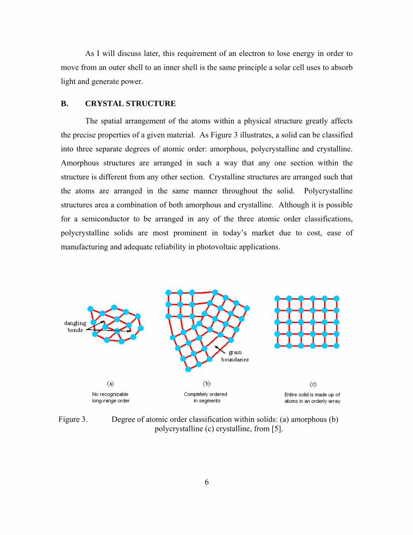
The spatial arrangement of the atoms within a physical structure greatly affects
the precise properties of a given material. As Figure 3 illustrates, a solid can be classified
into three separate degrees of atomic order: amorphous, polycrystalline and crystalline.
Amorphous structures are arranged in such a way that any one section within the
structure is different from any other section. Crystalline structures are arranged such that
the atoms are arranged in the same manner throughout the solid. Polycrystalline
structures area a combination of both amorphous and crystalline. Although it is possible
for a semiconductor to be arranged in any of the three atomic order classifications,
polycrystalline solids are most prominent in today’s market due to cost, ease of
manufacturing and adequate reliability in photovoltaic applications.
Figure 3. Degree of atomic order classification within solids: (a) amorphous (b) polycrystalline (c) crystalline, from [5].

7
The atomic structure of a semiconductor can be further described by its lattice
structure within a unit cell. The typical way to describe an atomic structure is to use the
Brevais lattice system, which describes the symmetry of a crystal by the three-
dimensional (3-D) geometric arrangement of the atoms in it. Although there are seven
separate categories within the Brevais system with fourteen total arrangements, the
simplest of the arrangements can be divided into three categories: the simple cubic, body-
centered cubic and face-centered cubic (Figure 4).
Figure 4. Brevais lattice cubics, from [6].
Taking a closer look at the lattice structure of an element with four valence
electrons, such as carbon, silicon and germanium, there are small differences from the
lattice structures described above and those of the group IV elements (those with four
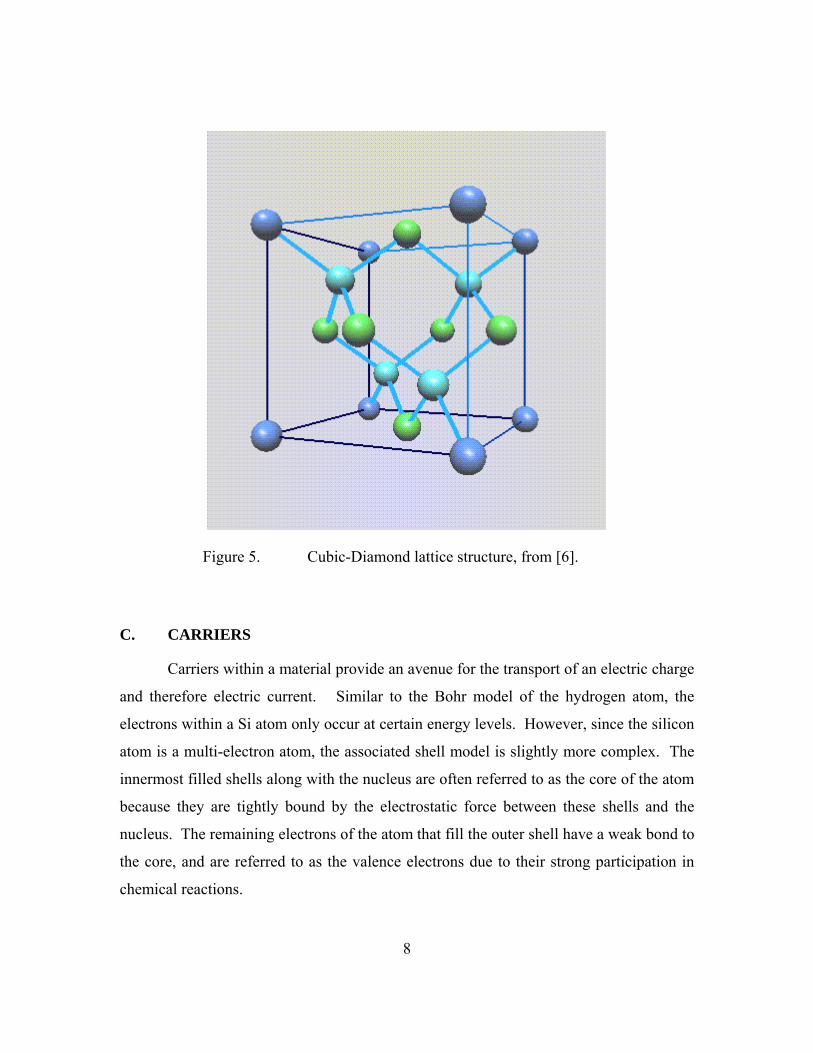
valence electrons). Figure 5 is a diamond lattice in which two face centered cubic lattices
are interpenetrating. The blue and green spheres represent the first interpenetrating face
centered cubic and the light blue sphere represents the second interpenetrating face
centered cubic. The second face centered cubic is diagonally shifted ¼ of the unit
distance. All element IV semiconductors are described as having cubic-diamond lattice
and are so named because each falls under the carbon element, which is the basic
building block of diamond. Within this lattice structure each atom is equidistant from its
four nearest neighbors. Silicon’s and germanium’s lattice constants are 5.437 Å and
5.660 Å respectively.
8
Figure 5. Cubic-Diamond lattice structure, from [6].
C. CARRIERS
Carriers within a material provide an avenue for the transport of an electric charge
and therefore electric current. Similar to the Bohr model of the hydrogen atom, the
electrons within a Si atom only occur at certain energy levels. However, since the silicon
atom is a multi-electron atom, the associated shell model is slightly more complex. The
innermost filled shells along with the nucleus are often referred to as the core of the atom
because they are tightly bound by the electrostatic force between these shells and the
nucleus. The remaining electrons of the atom that fill the outer shell have a weak bond to
the core, and are referred to as the valence electrons due to their strong participation in
chemical reactions.

9
Silicon has fourteen electrons, ten of which occupy the two inner most shells
(atom core) leaving four valence electrons. When the lattice is formed between the
different atoms, there is a finite probability that at any temperature above zero Kelvin
(0K), an electron from the valence band will be knocked free and an electron deficiency
known as a hole will be left behind. The hole left behind retains a positive charge equal
to the absolute value of the electron charge. The free electron along with the hole is
known as an electron hole pair (EHP) and can be described by the phenomenon of
ionization or generation. When a free electron and hole combine they disappear, a
process which is known as recombination. The rate of recombination is proportional to
the number of free electrons and existing holes. When in thermal equilibrium the
generation and recombination keep the number of EHPs constant. Germanium reacts in
much the same way although it has thirty-two total electrons, twenty-eight of which
constitute the atom core, leaving four valence electrons. Recombination and generation
will be discussed in more detail later.
An intrinsic material has no impurities (doping) in it and will not produce EHPs at
0K. However, the EHPs will increase logarithmically as a function of temperature
(Figure 6) and therefore conductivity will also increase.

10
Figure 6. Intrinsic carrier density vs. Temperature, from [7].
D. ENERGY BANDS
The energy band model is a useful way to visualize the differences between an
insulator, conductor and semiconductor (Figure 7). When looking at a material rather
than a free atom, the electrons within the material form energy bands known as a valence
band and conduction band at a specific energy state. The difference between the valence
and conduction band is known as the bandgap. The conductivity of a material is
dependent on the number of free electrons in the conduction band.
An insulator has a large bandgap that an electron must overcome in order for it to
flow in the conduction band. Conversely, a conductor is described as material with the
valence and conduction bands overlapping in which case the free electrons do not require
any energy to traverse an energy barrier. As expected, a semiconductor has a bandgap
that is not overlapping yet the energy difference between the valence and conduction
band is minimal.

11
Figure 7. Energy band diagrams, from [8]
Within the energy band there is a distinction between a direct bandgap and an
indirect bandgap based on the relative momentum between the valance band hole and the
conduction band electron. A direct bandgap semiconductor is one in which the maximum
energy level of the valence band and the minimum energy of the conduction band occur
at the same momentum. Examples of direct bandgap semiconductors are GaAs and InP
which are sometimes referred to as radiant recombination semiconductors because of the
band-to-band recombination and release of energy in the form of photons or radiation
wavelengths of light.
Indirect bandgap semiconductors have maximum and minimum energy band
levels at different momentums. Examples of indirect bandgap semiconductors are Si, Ge
and GaP. The energy released during indirect recombination cannot be direct band-to-
band and requires the assistance of a third party or defect in the material. This energy is
given off in the form of phonons or quasi-particles of quantized sound waves. The
energy band structure for Ge, Si and GaAs are compared in Figure 8. This relationship
will become more clear when discussing recombination and generation.

12
Figure 8. Energy band structure vs. wave vector for Ge, Si and GaAs, from [7].
E. INTRINSIC SEMICONDUCTORS AND DOPING
An intrinsic semiconductor is one with no impurities in it. Therefore, it exhibits
properties inherent to the pure semiconductor sample which can be used to identify the
material. Under equilibrium conditions, an intrinsic semiconductor has an equal number
of holes (p) and electrons (n) which is ultimately equal to the intrinsic carrier
concentration ( in ). The number of p and n are equal in an intrinsic semiconductor
because carriers are only created in pairs in a highly pure material. If an intrinsic
semiconductor bond is broken, a free electron and a hole are created simultaneously.
Similarly, if an electron is excited from the valence band to the conduction band then a
hole will simultaneously be created in the valence band. A list of common
semiconductor materials and their intrinsic carrier concentrations at room temperature are
Ge Si GaAs

13
given in Table 1. Although these concentrations may seem high, they are only a small
fraction of the total number of bonds in the respective materials.
Table 1. Intrinsic carrier concentration at room temperature (300K).
Carrier Concentration ( in ) per 3cm Material
62 10× GaAs
101 10× Si
132 10× Ge
Adding impurity atoms to a material changes its electrical properties, a process
known as doping. Doping is used to control the number of electrons or holes in a
material by the addition of a controlled amount of a specific impurity atom. The doping
of intrinsic material results in either a p-type or an n-type material, meaning it has an
excess number of holes or electrons respectively. With respect to IV elements, acceptors
(III elements) are added to produce a p-type material and donors (V elements) are added
to produce n-type materials. This is due to the number of valence electrons in the dopant
atom. From Section II.A we know that IV elements have four valence electrons. If an
element with three valence electrons is added to the diamond lattice the three valence
electrons will not be able to complete all of the semiconductor bonds with the element IV
atoms. Therefore, the excess electron will continue to be accepted by the dopant atom,
and an excess hole will be allowed to wander throughout the structure without the
creation of a free electron. Conversely, if a donor is added to the intrinsic element IV
material then all the semiconductor bonds will be made, leaving an excess electron to
roam throughout the lattice. Only a small amount of dopant, on the order of one atom for
every 1610 atoms, is required to significantly affect the electrical properties of a material.

14
F. FERMI LEVEL
The Fermi level describes the top of the collection of electron energy levels at 0K
and is based on the Fermi-Dirac probability equation (Eqn. 2.3). The Fermi-Dirac
probability equation is a particle statistic function that determines the distribution of
fermions (particles with half-integer spin) at a particular energy state at absolute zero.
( )1( )
1FE E kTf Ee −
=+
Eqn. 2.3
At 0K all the available energy states below FE will be filled by fermions of one
and only one particle which are constrained by the Pauli Exclusion Principle. At low
temperatures, any energy below the Fermi level will have a probability of 1 and any
energy above the Fermi level will have a probability of essentially 0. As the temperature
rises, EHPs are created and electrons of higher energy than the Fermi energy emerge in
the conduction band. Figure 9 illustrates this distribution for increased temperatures in an
intrinsic material.

15
Figure 9. Fermi distribution function, from [5].
The Fermi level can be manipulated by doping the material either with an
acceptor or donor, resulting in a p-type or n-type semiconductor respectively. By raising
or lowering the Fermi level, one can specify the required energy for an electron to
transition from the valance band to the conduction band. As in Figure 10, an intrinsic
material has a Fermi level at the center of the band gap. An n-type material shifts the
Fermi level closer to the conduction band producing shallow donors. Similarly, a p-type
material shifts the Fermi level closer to the valence band producing shallow acceptors.
With the Fermi level closer to the valence and conduction bands, only a small amount of
energy is required to ionize a hole or electron into their respective bands.
EF E
T0
T1
T2
T3
T0 = 0oK T0< T1< T2< T3

16
Figure 10. Schematic band diagram, density of states, Fermi–Dirac distribution and the carrier concentrations for intrinsic, n-type and p-type semiconductors at thermal
equilibrium, from [7].
Eg
EC
EV
E
EF
E E E
n
p
Eg
EC
EV
EF n–type
n
p
NDED
Eg
EC
EV
EF
density of states f(E) carrier concentratio
p–type
p
n
NAED

17
When the material is not under equilibrium conditions the Fermi level is
influenced creating Quasi-Fermi energy levels ( FnE and FpE ) described by the
distributions in Equation 2.4 and Equation 2.5. It is easy to see from these two equations
that at equilibrium F Fn FpE E E= = .
( )1( )
1Fnn E E kTf Ee −
=+
Eqn. 2.4
( )1( )
1Fpp E E kT
f Ee −
=+
Eqn. 2.5
As I will discuss later with respect to the tunneling effect, it is also possible to
degenerately dope the material in order to push the Fermi level into the valence or
conduction band. However, it is important to note that a heavily doped material may
exhibit unintended electrical properties depending on the distribution of the dopant.
Because the distribution of the dopant may not be homogenous throughout, different
energy fluctuations may be found at different positions within a strongly compensated
semiconductor. This is due to the mismatch of the lattices between the two materials,
which can greatly affect the conductivity of a material.
G. MOBILITY
Mobility (µ) is the ratio of average speed (drift speed) to the applied field of a
material and is analogous to permittivity ( sε ). Ideally (in a vacuum) an electron inside of
an electric field will continuously accelerate. However, in a material the electron will
accelerate only until it collides with an atom in the lattice. As expected, the higher
doping in a material will result in a higher probability of a collision with atoms in the
lattice and therefore mobility will decrease. Figure 11 illustrates this point for some
common semiconductors.

18
Figure 11. Mobility vs. doping level, from [7].
H. CURRENT DENSITY
The total particle current in a material is equal to the total current density (J) of
both the holes ( PJ ) and electrons ( NJ ) which results from the drift and diffusion current
densities. Diffusion current ( DI ) is the result of electrons or holes in a concentrated area
spreading themselves evenly though a material (Figure 12) in order to achieve a zero
μ [c
m2 /V
⋅s]
μ [c
m2 /V
⋅s]
μ [c
m2 /V
⋅s]
doping level [cm–3]
Si
Ge
GaAs
μn: electron mobility μp: hole mobility

19
concentration gradient ( 0n∇ = for holes, 0p∇ = for electrons) throughout. Diffusion
current density ( P diffJ for holes, N diffJ for electrons) is analogous to the majority carrier
concentration (doping) of a material and is described by Equation 2.6 and Equation 2.7
where PD and ND are the constants of proportionality.
Figure 12. Diffusion current, from [2].
PP diffJ qD p= − ∇ Eqn. 2.6
NN diffJ qD n= ∇ Eqn. 2.7
Drift current ( SI ) is the result of the introduction of an electric or magnetic field
and is analogous to the minority carrier concentration and is proportional to the intensity
of the field ( E ). Figure 13 illustrates drift current in the presence of an electric field and
Equation 2.8 and Equation 2.9 describe the mathematical model of drift current as a
function of mobility (µ) and applied electric field.
ID

20
Figure 13. Drift current in the presence of an electric field, from [2].
P driftJ pq pμ= X Eqn. 2.8
N driftJ Nq nμ= X Eqn. 2.9
Both the electron ( Nμ ) and hole ( pμ ) current densities depend on their associated
diffusion and drift currents (Eqn. 2.10 and Eqn. 2.11) which ultimately lead to the total
current density (Eqn. 2.12).
P PP drift P diffJ J J pq p qD pμ= + = − ∇E Eqn. 2.10
N NN drift N diffJ J J nq n qD nμ= + = − ∇E Eqn. 2.11
N PJ J J= + Eqn. 2.12
I. GENERATION AND RECOMBINATION
Generation is the process whereby electrons and holes (carriers) are created.
Conversely, recombination is the process whereby electrons and holes are annihilated.
Both generation and recombination are order-restoring mechanisms to return the system
to its equilibrium state (p=n= in ) after the carrier excess or deficit in the semiconductor is
stabilized or eliminated.
IS
––––––
++++++

21
There are three important recombination-generation methods as shown in Figure
14. Band-to-band recombination (a) is the direct annihilation of a valance band hole and
a conduction band electron when the hole and electron stray into the same vicinity within
the semiconductor lattice. The loss of energy experienced by the electron must release an
energy quantum equal to the total energy lost. This loss is typically realized in the form
of light as described in Equation 2.2.
The R-G (recombination-generation) center recombination is caused by defects or
special impurity atoms within the lattice and takes place only in special locations within
the semiconductor known as R-G centers. The R-G center concentration is typically very
low compared to the donor and acceptor concentration yet leads to the introduction of
various energy levels near the center of the band gap known as the trap energy ( TE ).
The R-G center recombination is a two-step process and can take place in one of two
ways as represented in Figure 14(b). The first method is when a carrier (hole or electron)
is trapped at the impurity location until the opposite carrier is attracted to the first and
recombination annihilates them both. The second is when an electron falls into the
impurity location where it will initially lose energy equal to T CE E− . Once a hole
comes into vicinity, the electron is attracted into the valence band after which it will lose
the rest of its energy equal to T VE E− before it recombines with the hole and disappears.
This type of recombination will cause quantum lattice vibrations which will release
thermal energy and ultimately increase the temperature of the semiconductor.
The third process is called Auger recombination (c), which is also a band-to-band
recombination. However, this process occurs simultaneously with a collision between
two like carriers. The energy transferred between the colliding carriers forces one carrier
into the alternate energy band while the second carrier remains in the original band. The
second carrier becomes highly energetic and then returns to its original energy level in
small heat producing steps as it collides with the semiconductor lattice. This unique
stepwise energy loss or “staircase” is defined as thermalization and also leads to an
increased semiconductor temperature.

22
Figure 14. Energy band visualization of recombination and generation processes, from [5].
The generation process is simply the reverse of the recombination process. For
band-to-band generation (d), thermal energy or light energy ( )ph GE E> absorbed by a
semiconductor will excite electrons from the valence band into the conduction band
creating an EHP. Similarly, for R-G center generation (e), thermal energy absorbed by
the semiconductor will excite the electron enough to achieve the trap energy at the
impurity location and then again to the conduction band. Carrier generation via impact

23
ionization (f) is analogous to Auger recombination, because the creation of EHPs is the
result of energy released when a highly energetic carrier collides with the semiconductor
lattice.
J. SUMMARY
The basic understanding of semiconductor physics leads to a more advanced
discussion of a p-n junction, which is discussed in the next chapter.

24
THIS PAGE INTENTIONALLY LEFT BLANK

25
III. P-N JUNCTIONS
A. INTRODUCTION TO JUNCTIONS
The successful implementation of a P-N junction is critical in modern electronics
and semiconductor devices, including bipolar junction and metal on oxide transistors
(BJT and MOSFET), rectifier and Zener diodes, and photovoltaics to name a few.
Through the doping process, a P-N junction is formed to effectively control the electrical
characteristics of a material.
B. BASIC STRUCTURE
A p-n junction is formed by a single crystal semiconductor where one side is
doped with acceptors (p) and the other side is doped with donors (n). At the location of
contact the metallurgical junction is formed as shown in Figure 15. Initially there is a
very large majority carrier density gradient at the metallurgical junction. Equilibrium
will be sought as the majority carriers in the p-type material (holes) will begin to diffuse
into the n-type material while the majority carriers from the n-type material (electrons)
will begin to diffuse into the p-type material.
Figure 15. (a) Simplified P-N junction; (b) doping profile, from [9].

26
The diffusing carriers from both regions will combine with the minority carriers
on the opposite side and disappear. Assuming that there is no outside electric field
connected to the junction, this diffusion can not continue indefinitely. The holes
diffusing from the p-region will leave behind negatively charged acceptor atoms and the
electrons diffusing from the n-region will leave behind positively charged donor atoms.
The net charges in the p- and n-regions will induce an electric field in the metallurgical
junction, which will form what is known as a space charge region or depletion region as
shown in Figure 16.
Figure 16. P-N junction depletion region formed by diffusion, from [9].
When in thermal equilibrium, the Fermi levels on both sides of the junction are
equal (Figure 17). The potential barrier known as a built in voltage ( biV ) is responsible
for maintaining equilibrium between the majority carrier electrons in the n-region and the

27
minority carrier electrons in the p-region. Similarly for the holes in the valence band, the
built in voltage maintains equilibrium between the majority carrier holes in the p-region
and the minority carrier holes in the n-region. As expected, the built in voltage depends
on doping levels ( aN and dN ) within the n- and p-regions (Eqn. 3.1).
Figure 17. P-N junction energy band diagram with Fermi level.
2ln a dbi
i
N NkTVq n
⎛ ⎞= ⎜ ⎟
⎝ ⎠ Eqn. 3.1
The width of the depletion region (W) is also related to the relative doping level
of the two regions. This characteristic will become more important with the
implementation of the tunnel junction (Section IV). The width of the depletion region (in
cm) can be calculated by using Equation 3.2.
1/ 22 s bi a d
a d
V N NWe N Nε⎧ ⎫⎡ ⎤+⎪ ⎪= ⎨ ⎬⎢ ⎥
⎪ ⎪⎣ ⎦⎩ ⎭ Eqn. 3.2

28
Applying different bias conditions between the two regions will disturb the p-n
junction from equilibrium and the Fermi levels will no longer remain constant. For a
standard doped junction, the three conditions of interest are reverse bias, forward bias and
the breakdown voltage.
C. REVERSE BIAS
Applying a negative voltage ( RV ) to the p-region with respect to the n-region
results in a reverse bias condition as shown in Figure 18. The voltage applied attracts the
majority carriers from their respective regions and leaves minority carriers in its place.
This increases the voltage barrier and widens the depletion region. The difference
between the two Fermi levels is equal to the bias voltage. Therefore, the total barrier
voltage ( totalV ) realized by the system is the sum of the built in voltage and bias voltage
(Eqn. 3.3). This barrier is easiest to visualize by the use of an energy band diagram in
Figure 19.
Figure 18. Reversed bias p-n junction schematic, from [2].

29
total bi RV V V= + Eqn. 3.3
Figure 19. Reversed bias p-n junction energy band diagram.
The depletion region width is given by Equation 3.4. When in reverse bias the
probability that an electron will gain enough energy to overcome the potential barrier is
very small and the junction will act like an insulator, not allowing current to flow. With
the increased depletion region, diffusion current (ID) is very small and the total current in
the system is approximately equal to the drift current (IS) (Eqn. 3.5). Ideally, this current
would be equal to zero, but, in reality, there is a small amount of drift current in the
system, as illustrated in Figure 20.
( )1/ 2
2 s bi R a d
a d
V V N NWe N N
ε⎧ ⎫+ ⎡ ⎤+⎪ ⎪= ⎨ ⎬⎢ ⎥⎪ ⎪⎣ ⎦⎩ ⎭
Eqn. 3.4

30
total S D SI I I I= + ≈ (very small) Eqn. 3.5
Figure 20. Reversed bias p-n junction I-V characteristic.
D. FORWARD BIAS
Applying a positive voltage ( aV ) to the p-region with respect to the n-region is
considered forward bias (Figure 21). The forward bias opposes the built in field
developed in the depletion region and the region becomes narrower. When the junction
is forward bias, the Fermi level in the p-region is increased and the Fermi level in the n-
region is decreased to a point where electrons can overcome the small potential barrier
(Eqn. 3.6), as illustrated by Figure 22.

31
Figure 21. Forward bias p-n junction schematic, from [2].
( bi aV V− ) Eqn. 3.6
total S D DI I I I= + ≈ Eqn. 3.7

32
Figure 22. Forward bias p-n junction energy band diagram.
As the continuously supplied majority carriers from the n-region transition into
the p-region, they become minority carriers where they diffuse and eventually combine
with the majority holes. Similarly, the continuously generated holes in the p-region will
be available to combine with the electrons traversing the potential barrier. Just as before,
some of the current being produced is due to drift (IS) and some is due to diffusion (ID).
However, in the forward bias condition the diffusion current is much greater than the drift
current (Eqn. 3.7) due to the decreased depletion region. Figure 23 shows the I-V
characteristic of a p-n junction in the forward bias condition. Notice that the current does
not begin to flow until sufficient voltage is applied to overcome the potential barrier.
This happens at approximately 0.7V for Si and 0.1V for Ge.

33
Figure 23. Forward bias p-n junction I-V characteristic.
E. BREAKDOWN/ZENER TUNNELING
Adding reverse bias beyond a certain threshold voltage will result in the
breakdown of the p-n junction. This breakdown phenomenon is due to either a Zener
effect or an avalanche effect.
The Zener or tunneling effect is similar to the tunneling which I will discuss at
length in the next section. The difference here is that the Zener effect takes place when a
minority carrier in the p-region valence band is able to penetrate through the energy
barrier to an empty state in the n-region conduction band unaffected. This can only occur
once the valence band of the p-region increases beyond the conduction band of the n-
region due to the reverse bias. The exchange of minority carriers creates a large change
in reverse current with a small change in reverse bias. Zener diodes are designed to
achieve this result (Figure 24).

34
Figure 24. Zener breakdown p-n junction I-V characteristic.
The avalanche effect is also a minority carrier effect in which an electron from the
p-region with a very large kinetic energy collides with atoms and breaks the covalent
bonds. Often the EHPs created collide with other atoms to create even more EHPs,
creating an avalanche-type effect. As more and more minority carriers are created, they
are swept to the opposite region which creates a large reverse current. This runaway
effect often leads to excess heat from the lattice vibrations and results in a damaged p-n
junction.
F. LOSSES
Ideally there would be no losses in the system and the slope of the I-V curve
would be perpendicular to the x-axis when on. However, since the semiconductor
material has an inherent ohmic resistance due to atomic masses and impurities, there is a
slight ohmic loss in the junction. Putting three regions together, a typical p-n junction I-
V curve is realized (Figure 25).

35
Figure 25. p-n junction I-V characteristic.
G. SUMMARY
Controlling the doping levels in the respective regions will shift the Fermi levels
and affect the ability of an electron or hole to move through the lattice. Increasing the
doping levels to a point where the Fermi levels are within the energy bands of the n- and
p- regions is essential to tunneling phenomenon and will be discussed in the following
Chapter.

36
THIS PAGE INTENTIONALLY LEFT BLANK

37
IV. TUNNEL JUNCTION
A. TUNNELING THEORY
The tunneling phenomenon is a majority carrier effect in which both the n- and p-
regions are degenerately doped (very heavily doped with impurities) allowing an electron
to tunnel through a potential barrier that, under normal conditions, would not be possible
to penetrate. The tunneling is based on a quantum transition probability ( tT ) per unit
time and is proportional to the exponent of the average value of momentum ( ( )0k ) within
the tunneling path across the depletion region (Eqn. 4.1). This momentum corresponds to
an incident carrier with a transverse momentum of zero and energy equal to the Fermi
energy. The tunneling probability equation will be further explained later in this section.
( )2
1
exp 2x
t xT k x dx
−
⎡ ⎤= −⎢ ⎥⎣ ⎦∫ Eqn. 4.1
B. PURPOSE
To achieve a higher power density, multiple cells with different I-V curves and
decreasing bandgaps are placed in tandem as illustrated in Figure 26. As a result the
incident light will be absorbed by the top cell allowing the unabsorbed photons to pass
through to the sub cells. This results in the sum of the voltage produced by the individual
cells.
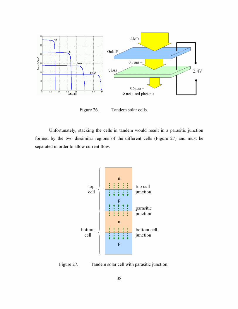
38
Figure 26. Tandem solar cells.
Unfortunately, stacking the cells in tandem would result in a parasitic junction
formed by the two dissimilar regions of the different cells (Figure 27) and must be
separated in order to allow current flow.
Figure 27. Tandem solar cell with parasitic junction.

39
One option is to mechanically stack the cells using an oxide/conductor contact as
shown in Figure 28. However, the added contact material shadows the sub cells from the
unused photons being passed through the top cell, limiting any efficiency gained by
placing the cells in tandem.
Figure 28. Tandem solar cell example with oxide/conductor contact separation, from [2].
Another solution to this issue is to use a tunnel junction to separate the individual
cells in the tandem cell. The tunnel junction will allow photons to pass through as well as
pass current with minimal voltage loss (Figure 29).

40
Figure 29. Tandem cell with tunnel junction.
C. THE JUNCTION
A tunnel junction is simply a tunnel diode or degenerately doped p-n junction
commonly used in switching and oscillator circuit applications. The difference between
the tunnel junction and the tunnel diode is that the tunnel junction is grown as a single
crystal joining two solar cells, whereas a tunnel diode operates as a discrete component
within a circuit. The purpose of mentioning the tunnel diode is for completeness, as
tunnel diodes have been studied and used in electronics since their invention by Leo
Esaki in 1958, who received the Nobel Prize in Physics in 1973 for his work. From this
point on, there will be no distinction made between the two and I will focus on the tunnel
junction and its application to photovoltaics.
A tunnel junction is formed with degenerately doped regions in order to push the
respective Fermi levels into the valence and conduction bands (Figure 30). As a result,
the p-region valence band will contain holes and the n-region conduction band will

41
contain electrons at thermal equilibrium. The depletion region width is also affected by
the degenerately doped regions compressing it to <100Å, which is essential to the
tunneling effect and is significantly smaller than a conventional p-n junction.
Figure 30. Degenerately doped tunnel junction energy band diagram.
In order for quantum tunneling to occur, four criteria must be met. The necessary
conditions for tunneling are: (1) occupied energy states exist on the side from which the
electron will tunnel; (2) unoccupied energy states exist at the same energy levels as those
electrons in the occupied energy states; (3) the tunneling barrier width is small and the
potential barrier height is low enough that there is a finite tunneling probability; and (4)
the momentum is conserved in the tunneling process [2].
D. THERMAL EQUILIBRIUM
As in the conventionally doped p-n junction, the two Fermi levels of the p- and n-
regions are equal at thermal equilibrium. Figure 31 illustrates the tunneling junction
energy bands at thermal equilibrium as well as the corresponding I-V plot. The red dot

42
on the I-V plot corresponds to the location of interest on the curve. Since both regions
are doped to the point where the Fermi levels exist inside the valence and conduction
band and are therefore considered degenerately doped.
Figure 31. Tunnel junction energy band and I-V characteristic at thermal equilibrium, from [7].
E. REVERSE BIAS
Similar to the Zener effect discussed in the last section, in reverse bias the
minority carrier in the p-region valence band is able to tunnel through the potential
barrier to the conduction band of the n-region. Unlike the Zener effect in a standard p-n
junction, the reverse bias tunneling in this junction occurs as soon as a reverse bias is
applied to the junction. The reason for the immediate response is the degenerate doping
of the regions. Since the Fermi levels are inside the respective valence and conduction
bands at equilibrium, there are empty states available for the minority carrier to fill as
soon as reverse bias is applied. Therefore, a large reverse current is realized for a small
change in voltage. Figure 32 illustrates the minority carrier electron tunneling to the
conduction band of the n-region as well as the location on the I-V curve where reverse
bias tunneling takes place.

43
Figure 32. Tunnel junction energy band and I-V characteristic in forward bias (reverse bias), from [7].
F. FORWARD BIAS
At forward bias (Figure 33), the tunnel junction has available energy states in the
p-region corresponding to filled energy states in the n-region. As the voltage is increased
from zero to pV , the valence band energy of the p-region and the conduction band energy
of the n-region become closer in value.

44
Figure 33. Tunnel junction energy band and I-V characteristic in forward bias (peak tunneling), from [7].
G. NEGATIVE RESISTANCE
From pV to vV , tunneling is still occurring but fewer and fewer empty states are
available. With a small increase in forward bias (> pV ), the number of electrons in the n-
region directly opposite the empty states in the p-region continues to decrease which will
result in a decreased tunneling current. The region from pV to vV is described as
negative resistance (Figure 34) and will continue until the valence band of the p-region is
equal to the conduction band of the n-region at which time the tunneling current will be
zero.

45
Figure 34. Tunnel junction energy band and I-V characteristic in forward bias (negative resistance), from [7].
H. THERMAL CURRENT FLOW
Increasing the forward bias even further beyond vV will eventually result in the
normal current flow of a p-n junction. As illustrated in Figure 35, the energy band
diagrams of the p- and n-regions are reminiscent of the standard p-n junction with an
applied forward bias. The relationship between a standard p-n junction and a
degenerately doped tunnel junction can be further understood by comparing the two
curves in Figure 36. As additional forward bias is applied, the current flow of the
standard p-n junction and that of the tunnel junction merge.

46
Figure 35. Tunnel junction energy band and I-V characteristic in forward bias (thermal current flow), from [7].
Figure 36. Characteristic I-V curve of a tunnel (red) and conventional (blue) p-n junction.

47
I. DIRECT AND INDIRECT TUNNELING
Just as there is a direct and indirect materials relationship, so too is there a direct
and indirect tunneling process. Superimposing the E-k relationship at the classical
turning points onto the E-x relationship of the tunnel junction reveals the direct and
indirect tunneling differences. In Figure 37 (a) and (b) the electrons in the vicinity of the
minimum of the conduction band energy-momentum can tunnel to a corresponding value
of momentum in the vicinity of the valence band. However, the distinction lies in the
electron and hole momentum.
For direct band tunneling to occur, the momentum for the valence band maximum
and the conduction band minimum must be the same. This type of tunneling is illustrated
in Figure 37 (a) and takes place in direct bandgap semiconductors such as GaAs and InP
as well as indirect bandgap semiconductors where the voltage applied to the junction is
large enough that the valence band maximum (Γ point) is in line with the conduction
band minimum (Γ point) [7].
Conversely, indirect band tunneling occurs when the conduction band minimum
and the valence band maximum do not occur at the same momentum, as shown in Figure
37 (b). As a result, momentum is conserved by scattering agents such as photons or
impurities and is deemed photon assisted tunneling. Due to the complex nature of photon
assisted tunneling, it is far less likely to take place when direct tunneling is possible.
However, it is possible for both direct and indirect tunneling to occur at the same time.

48
Figure 37. (a) Direct band tunneling process. (b) Indirect band tunneling process,
from [7]
J. TUNNELING CURRENT
For quantum tunneling to exist, the electric field in the depletion region must be
on the order of 610 V/cm. When this is achieved, there is a finite probability that an
electron will be excited from the valence band directly to the conduction band of the
semiconductor.
Local band-to-band tunneling models in Silvaco’s ATLAS© account for the
electric field at each node to calculate the generation rate due to tunneling. However, in
reality the tunneling is non-local and it is therefore necessary to take the spatial profile of
the energy bands into account as well as the spatial separation of the electrons generated
in the conduction band from the holes generated in the valence band [9]. To achieve this,
ATLAS© creates a series of 1-D slices through the device to calculate the tunneling

49
current. The slices are generated as an additional mesh through a series of qty and qtx
statements, which are then placed over the top of the original mesh. We will discuss the
mesh statements in detail in Section V.
With sufficiently high doping of both the p- and n-region of the junction, any
electron within the appropriate energy range has a finite probability of tunneling from the
valence band to the conduction band. ATLAS© considers each energy level within this
range and calculates the spatial start ( 1x− ) and end ( 2x ) point at that level. The tunneling
current can then be calculated as a function of the tunneling probability ( ( )T E ), the
effective mass (m*), and the potential barrier height ( gE ) as described by Equation 4.2,
where k is Boltzmann’s constant, q the electric charge, T is temperature, h is the reduced
planks constant and E is the electron energy.
( ) ( ) [ ][ ]2 3
1 exp* ln2 1 exp
Fl
Fr
E E kTqkTmJ E T E EE E kTπ
⎧ ⎫+ −⎪ ⎪= Δ⎨ ⎬+ −⎪ ⎪⎩ ⎭h Eqn. 4.2
ATLAS© provides the tools to implement a number of probability equations for
both local and non-local tunneling but none proved better at achieving the forward bias
than the Wentzel-Kramers-Brillouin method (WKB).
K. WENTZEL-KRAMERS-BRILLOUIN METHOD (WKB)
The tunneling probability is given by the WKB method (Eqn. 4.3) in which the
wave vector ( ( )k x ) of a carrier is evaluated as an exponential function and integrated
over the depletion region from 1x− to the 2x .
( )2
1
exp 2x
t xT k x dx
−
⎡ ⎤−⎢ ⎥⎣ ⎦∫ Eqn. 4.3
50
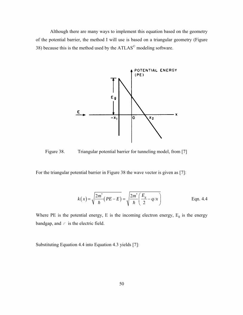
Although there are many ways to implement this equation based on the geometry
of the potential barrier, the method I will use is based on a triangular geometry (Figure
38) because this is the method used by the ATLAS© modeling software.
Figure 38. Triangular potential barrier for tunneling model, from [7]
For the triangular potential barrier in Figure 38 the wave vector is given as [7]:
( ) ( )* *2 2
2gEm mk x PE E q x
⎛ ⎞= − = −⎜ ⎟
⎝ ⎠h hE Eqn. 4.4
Where PE is the potential energy, E is the incoming electron energy, Eg is the energy
bandgap, and E is the electric field.
Substituting Equation 4.4 into Equation 4.3 yields [7]:
51
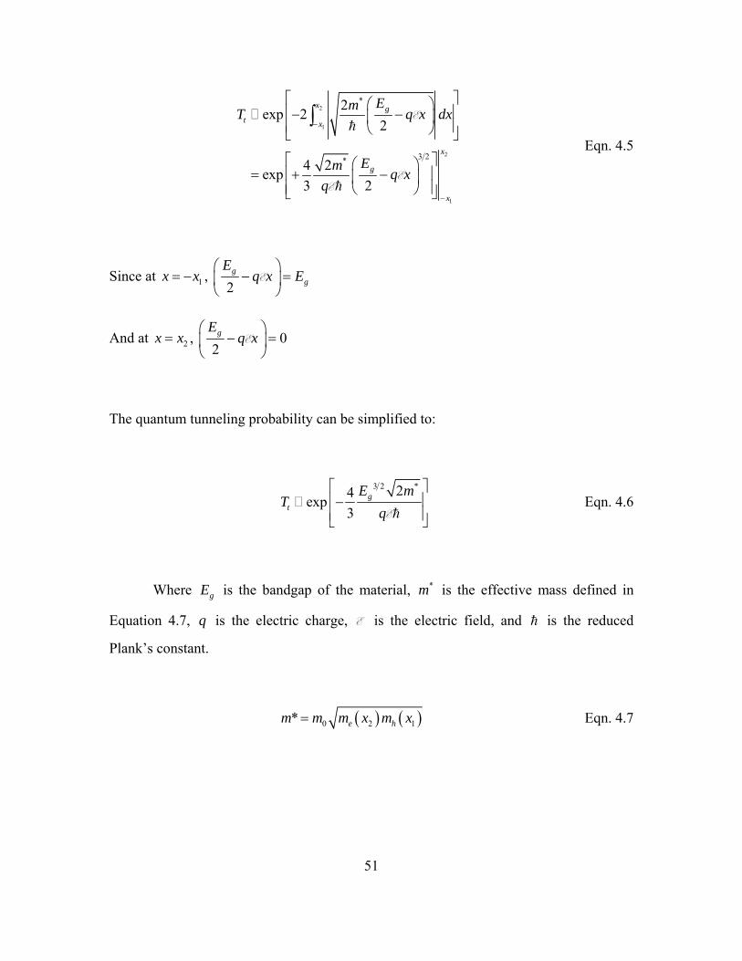
2
1
2
1
*
3 2*
2exp 22
4 2exp3 2
x gt x
x
g
x
EmT q x dx
Em q xq
−
−
⎡ ⎤⎛ ⎞⎢ ⎥− −⎜ ⎟⎢ ⎥⎝ ⎠⎣ ⎦
⎡ ⎤⎛ ⎞= + −⎢ ⎥⎜ ⎟
⎢ ⎥⎝ ⎠⎣ ⎦
∫ h
h
E
EE
Eqn. 4.5
Since at 1x x= − , 2
gg
Eq x E
⎛ ⎞− =⎜ ⎟
⎝ ⎠E
And at 2x x= , 02
gEq x
⎛ ⎞− =⎜ ⎟
⎝ ⎠E
The quantum tunneling probability can be simplified to:
3 2 *24exp3
gt
E mT
q
⎡ ⎤⎢ ⎥−⎢ ⎥⎣ ⎦hE
Eqn. 4.6
Where gE is the bandgap of the material, *m is the effective mass defined in
Equation 4.7, q is the electric charge, E is the electric field, and h is the reduced
Plank’s constant.
( ) ( )0 2 1* e hm m m x m x= Eqn. 4.7

52
L. SUMMARY
The tunneling phenomenon presented is based on the probability that an electron
is able to penetrate a potential barrier if there are occupied and unoccupied states at the
same energy level on both sides of the potential barrier, the distance between the
beginning and end of the potential barrier is sufficiently small, and momentum of the
tunneling electron is conserved. The following Chapter will implement the given
equations into the Silvaco software.

53
V. SIMULATION SOFTWARE
A. SILVACO
Silicon Valley Company (Silvaco) is a leading vendor in technology computer
aided design (TCAD). Established in 1984 and located in Santa Clara, California,
Silvaco has developed a number of exceptional CAD simulation tools to aid in
semiconductor process and device simulation. Silvaco has an extensive support team to
assist with the broad array of semiconductor technologies.
B. ATLAS©/DECKBUILD
The ability to accurately simulate a semiconductor device is critical to industry
and research environments. The ATLAS© device simulator is specifically designed for
2D and 3D modeling to include electrical, optical and thermal properties within a
semiconductor device. ATLAS© provides an integrated physics-based platform to
analyze DC, AC and time-domain responses for all semiconductor-based technologies.
The powerful input syntax allows the user to design any semiconductor device using both
standard and user-defined material of any size and dimension. ATLAS© also offers a
number of useful device examples to assist in your own unique design.
DeckBuild is the run time environment used to input a command file or deck and
is given the extension “.in”. To run ATLAS© in the DeckBuild environment, the user
must first call the ATLAS simulator with the command:
go atlas
There is other simulation software available that can be used in conjunction with
DeckBuild, such as ATHENA and DevEdit (Figure 39), but ATLAS© is the most
appropriate environment for this research.
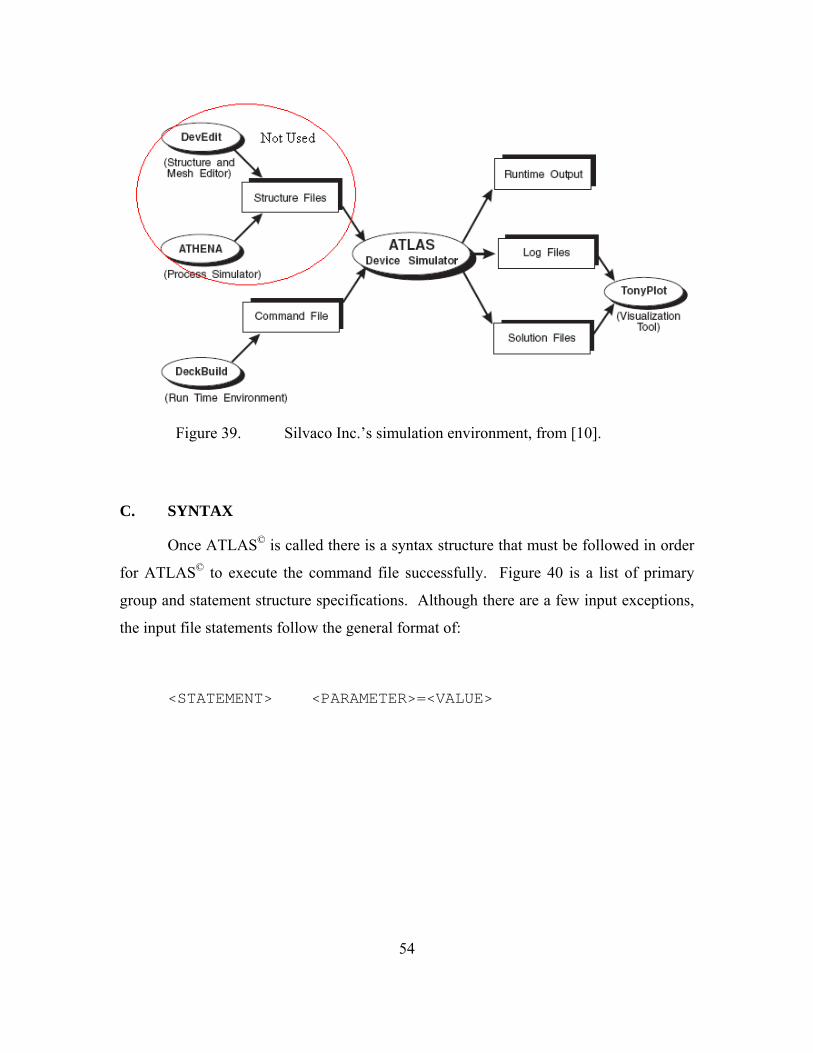
54
Figure 39. Silvaco Inc.’s simulation environment, from [10].
C. SYNTAX
Once ATLAS© is called there is a syntax structure that must be followed in order
for ATLAS© to execute the command file successfully. Figure 40 is a list of primary
group and statement structure specifications. Although there are a few input exceptions,
the input file statements follow the general format of:
<STATEMENT> <PARAMETER>=<VALUE>

55
Figure 40. ATLAS© command groups with the primary statements in each group, from [11].
D. STRUCTURE SPECIFICATION
1. Mesh
The mesh statement is used to define the structure in an inverted 2D or 3D
Cartesian grid. The x-axis is positive from left to right, the y-axis is negative from bottom
to top and the z-axis is positive from the plane of the x-y axis into the workspace. The
reason for the inverted y-axis is that the manufacturing coordinates are usually described
as depth below the surface. All coordinates are entered in microns and the spacing is
used to refine the sharpness and accuracy at an assigned location. ATLAS© produces a
series of triangles to form the mesh based on the user input parameters. Figure 41 shows
the mesh of a tunnel junction along with the parameters entered in ATLAS©.
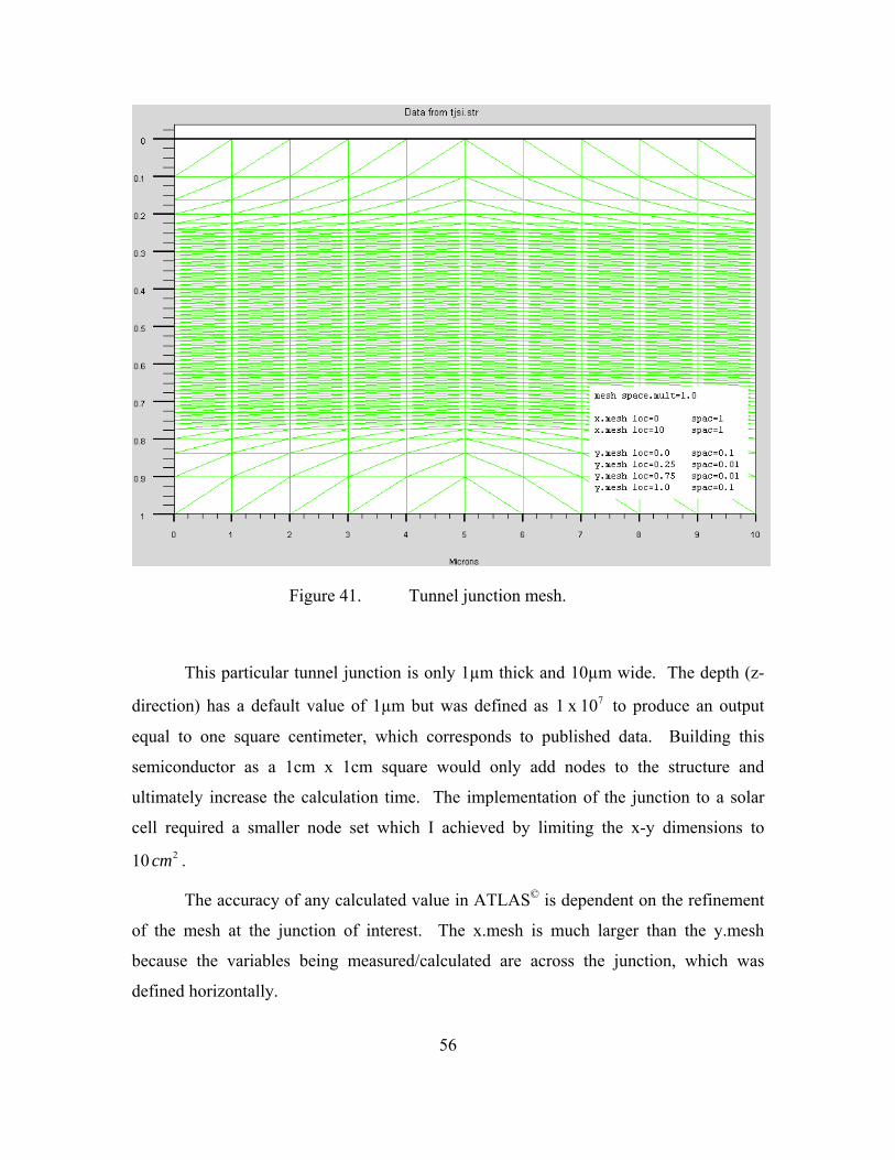
56
Figure 41. Tunnel junction mesh.
This particular tunnel junction is only 1µm thick and 10µm wide. The depth (z-
direction) has a default value of 1µm but was defined as 71 x 10 to produce an output
equal to one square centimeter, which corresponds to published data. Building this
semiconductor as a 1cm x 1cm square would only add nodes to the structure and
ultimately increase the calculation time. The implementation of the junction to a solar
cell required a smaller node set which I achieved by limiting the x-y dimensions to
10 2cm .
The accuracy of any calculated value in ATLAS© is dependent on the refinement
of the mesh at the junction of interest. The x.mesh is much larger than the y.mesh
because the variables being measured/calculated are across the junction, which was
defined horizontally.

57
2. Region
The region statement is used to separate the initial mesh statement into distinct
blocks and sets the initial material parameters that can be referred to later by region
number. All meshed areas of a structure must be assigned a region and the regions must
be ordered from lowest to highest region. For instance, region 5 cannot be defined before
region 4. The tunnel junction is described by the DeckBuild commands along with the
region lines in Figure 42.
Figure 42. Tunnel junction region.
3. Electrode
Once the regions are set, the electrodes must be assigned to the desired region so
that it can be electrically analyzed. The electrode can be assigned to any region or
portion of a region including the “top” or “bottom” as it is in this research. Because this
tunnel junction is intended to be used as an interconnect between two solar cells, it was

58
unnecessary to assign the electrodes to metal contacts or large areas that would constitute
superfluous calculations or error. Therefore, the anode was assigned to the top of the
junction and cathode was assigned to the bottom. The following statements were used to
define these parameters:
#electrodes
electrode name=anode top
electrode name=cathode bottom
4. Doping
The last required input of the structure specification is the doping statement. The
doping statement is used to assign the doping level within the previously assigned
regions. Various properties can be appended to the doping statement to specify how the
semiconductor was doped and of whether the region is n- or p-type. The desired I-V
relationship in forward bias will determine the doping characteristics of the
semiconductor. However, the following statements were developed for a Si junction with
a forward bias current of approximately 12A at 0.06V:
doping uniform p.type conc=5e19 y.max=0.5 doping uniform n.type conc=1e20 y.min=0.5
Here the regions were already defined in a previous statement and were therefore
referred to by their region number. Region 1 was uniformly doped with a p-type material
with a concentration of 5e19. Similarly, region 2 was uniformly doped with an n-type
material at a concentration of 1e20.
With the doping statement complete, the structure specifications are complete and
it is possible to continue with the simulation following the guidelines in Figure 40.
Unlike the structure specifications, the remaining four groups to be specified do not
require all statements to run without error.

59
E. QUANTUM TUNNELING MESH
In order to calculate the quantum tunneling through a potential barrier, finer slices
of the junction must be taken. ATLAS© does this with the definition of the qtx.mesh and
qty.mesh statements. The direction of tunneling must also be specified with a different
parameter in the models statement. Figure 43 illustrates the extremely refined qty.mesh
along with the input parameters to achieve this level of precision. Although the qtx.mesh
was defined, the slices are only extremely refined in the y-direction because this is the
direction of tunneling. The new rectangular mesh is superimposed over the original
triangular mesh and both mesh statements will be evaluated and accounted for in the
tunneling current. As with all ATLAS© spacing parameters, the qty.mesh spacing is
specified as µm.
Figure 43. Tunnel junction qtx.mesh and qty.mesh.

60
F. MATERIAL MODELS SPECIFICATION
1. Material
The material statement relates physical parameters with the materials assigned to
the mesh. The important material parameters for most standard semiconductors are
already defined by ATLAS© and therefore do not require any changes. We utilized the
extensive model libraries in ATLAS© since the developed tunnel junctions were based in
Si, Ge, and GaAs which are all very well researched and documented.
2. Models
The models statement is essential to the accurate modeling of a particular
phenomenon because it sets flags for ATLAS© to indicate the inclusion of different
mathematical models, physical mechanisms and other global parameters such as substrate
temperature. The model statement and parameters used in this research are listed below:
models temperature=300 srh fermi ni.fermi print qtunn.dir=0 \
bbt.nonlocal bbt.forward bbt.nlderivs
As with all ATLAS© statements, a complete list of modeling parameters and their
definitions can be found in the ATLAS© User’s Manual [11]. The most notable
parameters for the calculation of the quantum tunneling effect are qtunn.dir, bbt.nonlocal,
bbt.forward and bbt.nlderivs. qtunn.dir specifies the direction of tunneling across the
junction. Since this device was set up for tunneling across the y-axis, the parameter value
was set to zero (to specify tunneling in x-direction, qtunn.dir = 1). The bbt.nonlocal,
bbt.forward and bbt.nlderivs parameters enable the non-local band-to-band tunneling
model to be used in forward bias and allows the use of the non-local derivatives in the
Jacobian matrix which helps eliminate convergence problems.
3. Contact
Since the tunnel junction is meant to be used as an interconnect of a single crystal
multi-junction solar cell there was no need to specify any contact parameters. The

61
electrode statements assigning the cathode and anode to the semiconductor were
sufficient for calculating the current through the junction.
G. NUMERICAL METHOD SELECTION
The method statement specifies the numerical methods to be used in the
calculations specified in the model statement. The quantum tunneling through a junction
is highly dependent on the carrier concentration. Therefore, it is very important to
accurately measure the carrier concentration for each iteration. This is done by defining
the climit parameter in the method statement, which specifies the normalization factor to
limit the step size of the potential update. The parameter dvmax sets the maximum
allowed potential updates per iteration. Reducing dvmax dampens the oscillations in the
small I-V calculations.
H. SOLUTION SPECIFICATION
The log/solve/save statements are used to create data files in ATLAS©
simulations. These statements work together to be provide data to be analyzed by other
functions. This research I have used these three statements as a tool to check bias points,
energy band diagrams and carrier concentrations as a result of varying stimuli.
1. Log
The log statement allows all terminal characteristics generated by a solve
statement to be saved to a file.
2. Solve
The solve statement specifies which bias points are to be applied to produce an
output. The bias points can be set in a number of different way including step, initial and
lambda depending on what stimulus is desired.

62
3. Save
The save statement is used to save all node point data into an output file. A
common use of the log/solve/save statements for the tunnel junction studied is shown
below:
log outfile=tjsi.log
solve name=anode vanode =-1 vstep=0.1 vfinal=0.0
solve name=anode vanode =0.0 vstep=0.01 vfinal=0.2
solve name=anode vanode =0.2 vstep=0.1 vfinal=1.5
save outfile=tjsi.log
Here the output file tjsi.log has been set aside to store data from the solve
statements and then saved so that the data can be called at a later time. The solve
statements simply sweep the voltage from -1V to 1.5V in varying voltage steps
depending on the degree of accuracy at the desired range. With the date stored in an
outfile, it is ready to be displayed so that it can be analyzed.
I. RESULTS ANALYSIS
The tonyplot statement is used to start the graphical post-processor tool. Calling
tonyplot to visualize tjsi.log displays the output file in Figure 44. The complete tunnel
junction input deck can be found in Appendix A.

63
Figure 44. Silicon tunnel junction I-V curve in ATLAS©.

64
THIS PAGE INTENTIONALLY LEFT BLANK

65
VI. TUNNEL JUNCTION RESULTS
After the successful modeling of the basic forward bias tunneling current in Si, it
was necessary to test the validity of the model. This was accomplished by measuring the
response of different materials and doping levels to similar bias conditions.
A. SEMICONDUCTOR MATERIAL
As an interconnect between two dissimilar solar cells it is important that a tunnel
junction can be modeled for materials other than Si. Typical tunnel junctions used today
are GaAs and InGaP due to their close lattice matching. The ATLAS© input deck
presented here was developed so that cell parameters are easily changed and the tonyplot
outputs are easy to compare.
The doping levels’ initial calculations were based on the Fermi-Dirac equations
presented in Section II. Figures 45 and 46 illustrate the tunnel junction energy band
diagrams along with their associated I-V curves for GaAs and InGaP respectively.
Figure 45. GaAs tunnel junction (p = 3e20/cm3 n = 9e18/cm3) (A/cm2 versus volts in a 1µm thick junction).

66
Figure 46. InGaP tunnel junction (p = 2e20/cm3 n = 9e18/cm3) (A/cm2 versus volts in a 1µm thick junction).
By fine-tuning the doping levels, an output current of approximately 200mA was
realized for both junctions. Though this current is slightly high for a typical current
produced by a solar cell, we simply solved for 200mA as a baseline. With the successful
modeling of the two junctions, we were able to manipulate the doping levels and analyze
the different outputs.
B. TUNNEL JUNCTION DOPING
The doping levels of the tunnel junctions were changed for both the n- and p-
regions to shift the Fermi level and ultimately vary the response to the given bias
condition. Figures 47 through 52 illustrate the reaction to increased doping of the GaAs
junction. Figures 53 through 58 show similar results for an InGaP junction.
Initially, the p-region was varied from a doping level within 3kT (~0.077eV) of
the valence band, then increased by a reasonable factor (between 2 and 3) to show the
response in the I-V curve. Pushing the Fermi level further into the valence band

67
corresponds to an increased number of available holes that can recombine with electrons
tunneling through the junction and therefore increases the current.
The n-region was varied in a similar manner. However, pushing the Fermi level
further into the conduction band increases the number of electrons available to tunnel
through the junction and similarly increases the current.
1. GaAs Tunnel Junction
a. p-region variation:
Figure 47. GaAs IV characteristics and energy band diagram (p = 1e20/cm3 n = 9e18/cm3) (A/cm2 versus volts in a 1µm thick junction).

68
Figure 48. GaAs IV characteristics and energy band diagram (p = 3e20/cm3 n = 9e18/cm3) (A/cm2 versus volts in a 1µm thick junction).
Figure 49. GaAs IV characteristics and energy band diagram (p = 6e20/cm3 n = 9e18/cm3) (A/cm2 versus volts in a 1µm thick junction).

69
b. n-region variation:
Figure 50. GaAs IV characteristics and energy band diagram (p = 3e20/cm3 n =
6e18/cm3) (A/cm2 versus volts in a 1µm thick junction).
Figure 51. GaAs IV characteristics and energy band diagram (p = 3e20/cm3 n = 9e18/cm3) (A/cm2 versus volts in a 1µm thick junction).
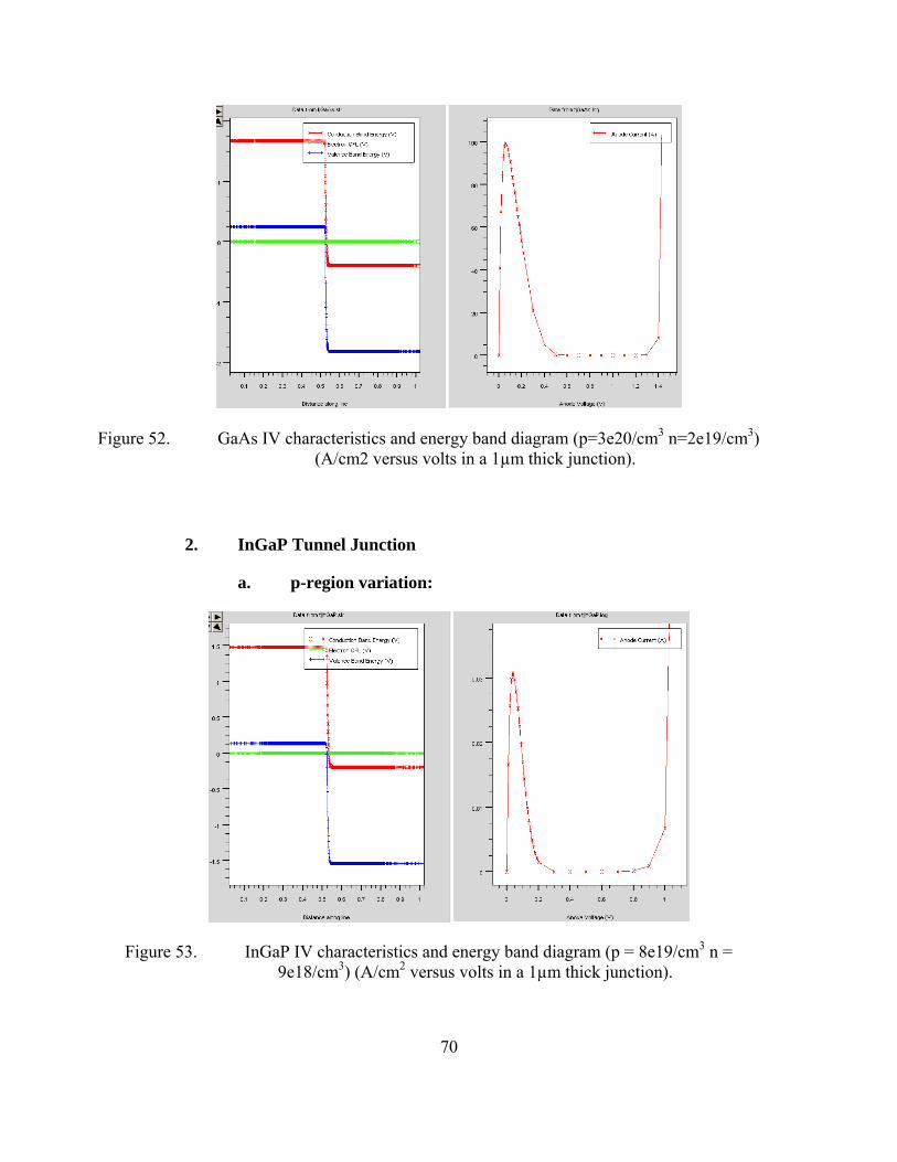
70
Figure 52. GaAs IV characteristics and energy band diagram (p=3e20/cm3 n=2e19/cm3) (A/cm2 versus volts in a 1µm thick junction).
2. InGaP Tunnel Junction
a. p-region variation:
Figure 53. InGaP IV characteristics and energy band diagram (p = 8e19/cm3 n = 9e18/cm3) (A/cm2 versus volts in a 1µm thick junction).

71
Figure 54. InGaP IV characteristics and energy band diagram (p = 2e20/cm3 n = 9e18/cm3) (A/cm2 versus volts in a 1µm thick junction).
Figure 55. InGaP IV characteristics and energy band diagram (p = 4e20/cm3 n = 9e18/cm3) (A/cm2 versus volts in a 1µm thick junction).

72
b. n-region variation:
Figure 56. InGaP IV characteristics and energy band diagram (p = 2e20/cm3 n = 6e18/cm3) (A/cm2 versus volts in a 1µm thick junction).
Figure 57. InGaP IV characteristics and energy band diagram (p = 2e20/cm3 n = 9e18/cm3) (A/cm2 versus volts in a 1µm thick junction).
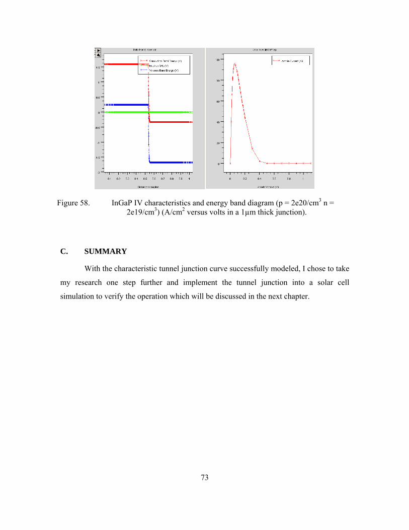
73
Figure 58. InGaP IV characteristics and energy band diagram (p = 2e20/cm3 n = 2e19/cm3) (A/cm2 versus volts in a 1µm thick junction).
C. SUMMARY
With the characteristic tunnel junction curve successfully modeled, I chose to take
my research one step further and implement the tunnel junction into a solar cell
simulation to verify the operation which will be discussed in the next chapter.

74
THIS PAGE INTENTIONALLY LEFT BLANK

75
VII. SOLAR CELL IMPLEMENTATION
The solar cell implementation was based on research completed by Panayiotis
Michalopoulos [2] in 2002. Michalopoulos was a student of Prof. Sherif Michael at the
Naval Postgraduate School and his research was developed using Silvaco software.
A. SOLAR RADIATION
The sun’s energy is derived from nuclear fusion reactions where 6 x 10¹¹kg of
hydrogen (H2) is converted to helium (He) every second. The mass lost due to the
conversion is approximately 4 x 10³kg. The energy produced by this loss can be
determined by Einstein’s famous mass-energy equation (E=mc2) and is found to be 4 x
1020J. This energy is emitted as electromagnetic radiation primarily at wavelengths from
the ultraviolet to infrared and radio spectra (0.2 - 3µm) [12].
The intensity of the sun’s energy depends on the location of where it is measured.
Outside the earth’s atmosphere, the intensity is measured to be approximately 1365W/m2
which produces a specific spectral response referred to as air mass zero (AM0). As the
energy transits the earth’s atmosphere, it is attenuated by ultraviolet absorption due to
ozone, scattering due to airborne dust, and infrared absorption due to water vapor. AM1
and AM1.5 is used for terrestrial applications with incident solar power ranging from 925
to 963W/m2.
B. I-V CURVE
As discussed in Chapter II, an electron must release energy to go from an outer
shell (higher energy state) to an inner shell (lower energy state). Conversely, if a certain
level of energy is absorbed, such as solar energy, an electron may transit from an inner
shell to an outer shell or valence shell. In an intrinsic semiconductor this creation of
carriers leads to an increase in conductivity. However, when a p-n junction is formed in a
semiconductor the carriers will separate to create electron hole pairs (EHPs). The
minority carrier will be swept across the junction due to the electrostatic field formed by
the depletion region and the excess majority carriers created by the photogeneration will

76
develop a voltage differential between the two regions. If the junction is then connected
to a load, current will flow (photocurrent). This phenomenon is known as photovoltaics
because of the voltage potential generated by the photon (solar) energy.
As photons generate EHPs in a p-n junction, the standard diode dark current
characteristic (Figure 59a-blue) is shifted down to produce the illuminated current
characteristic (Figure 59a-red). Because a solar cell is usually presented as a power
supply, the illuminated characteristic is most often reflected across the x-axis to show that
the photocurrent conventionally flows in the opposite direction of the standard diode
current (Figure 7.1b).
Figure 59. (a) Dark (blue) and illuminated (red) current characteristic curve of the solar cell. (b) Solar cell current characteristic curve with FF.
The number of EHPs generated in the semiconductor is proportional to the
photons entering the semiconductor. However, many of the EHPs recombine inside the
material before it is collected and are therefore not used to produce photocurrent. Thus,
the maximum obtained power ( obtainedP ) is less than the maximum theoretical power

77
( theoryP ). The ratio of obtained power to theoretical power is called fill factor or FF (Eqn.
7.1). The FF can be seen graphically in Figure 59 (b).
obtained max max
theory SC OC
P I VFF = =P I V
Eqn. 7.1
The power conversion efficiency (n) of a solar cell is given as the ratio of the
maximum realized power to the incident power ( incP ).
max SC OC
inc inc
P I V FFn = =P P
Eqn. 7.2
To maximize the power conversion efficiency, the FF, Voc and Isc must be
optimized.
C. SINGLE CELL
Initially a single cell for each material in the multi-junction cell was modeled in
ATLAS©. This simulation was based on the code already developed for a Naval
Postgraduate School thesis by Panayiotis Michalopoulos in March 2002. Both cells were
illuminated at AM0. The doping levels and thicknesses are illustrated in Figure 60 and
62 followed by their corresponding I-V curve (Figures 61 and 63).

78
Figure 60. Optimized InGaP cell structure.
Figure 61. Optimized InGaP I-V curve. (A/cm2 versus voltage).

79
Figure 62. Optimized GaAs cell structure.
Figure 63. Optimized GaAs I-V curve. (A/cm2 versus voltage).
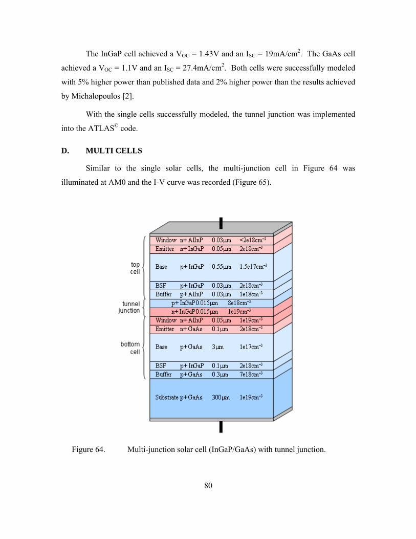
80
The InGaP cell achieved a VOC = 1.43V and an ISC = 19mA/cm2. The GaAs cell
achieved a VOC = 1.1V and an ISC = 27.4mA/cm2. Both cells were successfully modeled
with 5% higher power than published data and 2% higher power than the results achieved
by Michalopoulos [2].
With the single cells successfully modeled, the tunnel junction was implemented
into the ATLAS© code.
D. MULTI CELLS
Similar to the single solar cells, the multi-junction cell in Figure 64 was
illuminated at AM0 and the I-V curve was recorded (Figure 65).
Figure 64. Multi-junction solar cell (InGaP/GaAs) with tunnel junction.

81
Figure 65. Multi-junction solar cell (InGaP/GaAs) I-V curve. (A/cm2 versus voltage).
The multi-junction solar cell model achieved a VOC = 2.5V and an ISC =
18.7mA/cm2. As expected, the voltage is the sum of the two cells in the single cell
models accounting for the small voltage drop across the tunnel junction. Ideally, both
cells would generate the same current as in the single cell model and the realized current
in the multi-junction cell would be the lower of the two. However, because the higher
energy photons are absorbed by the InGaP top-cell, the GaAs bottom-cell is not able to
generate as many EHPs and therefore realizes a slightly smaller current than ideal.
Taking the research one step further, the tunnel junction was implemented in the
optimized multi-junction cell model. This was done so that the modeled output could be
compared to empirical data in [3]. The optimized cell has an antireflective coating to
absorb a greater number of photons and a back surface reflector to reflect some of the
unutilized photons back into the semiconductor material. These additions help to create
more EHPs and ultimately a higher current and power density.
Experimental data for an InGaP/GaAs photovoltaic cell produced a VOC = 2.488V
and an ISC = 23mA/cm2 [3]. The optimized multi-junction cell model achieved a VOC =
2.5V and an ISC = 22mA/cm2 with a FF = 84% and η = 29% (Figure 66). This is only

82
3.8% greater power density than the experimental data and demonstrates the ability to
model a tunnel junction for use in photovoltaic optimization.
Figure 66. Optimized multi-junction solar cell (InGaP/GaAs) I-V curve. (A/cm2 versus voltage)

83
VIII. RECOMMENDATIONS AND CONCLUSION
A. RECOMMENDATIONS
1. Physical Experiment
The tunnel junction model presented here has produced very promising results.
For this research the most important characteristic of the tunnel junction is the forward
bias electron tunneling which was successfully modeled using Silvaco Inc’s ATLAS©
software. Unfortunately, time and resources did not allow for a physical model
comparison. Although an implemented junction was compared to empirical values, the
tunnel itself was only compared to theoretical values and responses based on
mathematical models.
After further refinement and modeling, it is recommended that a project be funded
to produce a junction with the precise specifications so that it may be tested and
compared to the modeled parameters. Developing a more efficient tunnel junction and
continuing to test the accuracy of the models, will lead to the development of more
efficient solar cells.
2. Other Software
Throughout this study, a number of competing software programs were used in an
effort to model the forward bias response of a tunnel junction. Some were geared more
toward other aspects of the semiconductor industries such as MEMs design or computer
architecture and were therefore difficult to use to implement a tunnel junction into a solar
cell. Other programs were solar cell centric yet did not have the capacity or tools to
realize the quantum tunneling effect of the degenerately doped junction.
There are other software packages available that are comparable to Silvaco’s
ATLAS© and would be beneficial to this research. It is recommended that the utility of
these software packages be explored and compared.

84
3. Temperature and Radiation Effects
The use of photovoltaics in space applications is very important. Therefore, the
tunnel junction should be adapted and tested under extreme conditions to ensure the
accuracy of the model. The effects of temperature and radiation on a tunnel junction
should be explored to ensure no anomalies exist.
B. CONCLUSION
The value of using simulation software such as ATLAS© to model
semiconductors has revolutionized the semiconductor industry. Not only are time and
money saved by minimizing the need to manufacture and test changes to a design, but
efficiency is being pushed to the limit.
It has been have shown throughout this thesis that it is possible to model such
effects as quantum tunneling in a photovoltaic solar cell. To this point, the tunnel
junction in a multi-junction cell was modeled as a vacuum to insulate the layers, then
hardwired to pass the current between cells. Although this is effective, the cell being
modeled is not fully optimized.
A paper entitled “Multi-Junction Photovoltaic Model Optimizations for Space and
Solar Concentrator Applications” [13], was presented by Professor Michael and the
author on September 3, 2008, at the 23rd European Photovoltaic Solar Energy
Conference, that was held in Valencia, Spain. The paper focused on the application of
multi-junction photovoltaic cells using tunnel junction technology for use in space
applications. The tunnel junction modeling has the potential to push photovoltaic
technology to a new level of optimization and power density and it is necessary to model
this phenomenon accurately.

85
APPENDIX. ATLAS© SOURCE CODE
A. MAIN STRUCTURE
go atlas # Definition of constants # Mesh # X-Mesh # Y-Mesh # Regions # Electrodes # Doping # QT Mesh # Material properties # Models # Light beams # Solving
B. TUNNEL JUNCTION
go atlas
1. X-Mesh mesh width=1e7 #x-mesh x.mesh loc=0 spac=1 x.mesh loc=10 spac=1
2. Y-Mesh y.mesh loc=0.0 spac=0.01 y.mesh loc=0.25 spac=0.001 y.mesh loc=0.75 spac=0.001 y.mesh loc=1.0 spac=0.01
3. Regions region num=1 material=InGaP x.min=0 x.max=10 y.min=0.5 y.max=1 region num=2 material=InGaP x.min=0 x.max=10 y.min=0 y.max=0.5
4. Electrodes elec name=anode top elec name=cathode bottom doping uniform p.type conc=2e20 y.max=0.5 doping uniform n.type conc=2e19 y.min=0.5

86
5. QT-Mesh qtx.mesh loc=0 spac=1 qtx.mesh loc=10 spac=1 qty.mesh loc=0.35 spac=0.01 qty.mesh loc=0.5 spac=0.0005 qty.mesh loc=0.65 spac=0.01
6. Models/Output models temperature=300 srh fermi ni.fermi print \ qtunn.dir=0 bbt.nonlocal bbt.forward bbt.nlderivs output band.temp traps u.srh taurn taurp band.param con.band val.band \ qfn qfp log outfile=tjInGaP.str solve init save outfile=tjInGaP.str tonyplot tjInGaP.str method climit=1.0 dvmax=0.05 solve init solve prev log outfile=tjInGaP.log
7. Solve solve name=anode vanode =-1 vstep=0.1 vfinal=0.0 solve name=anode vanode =0.0 vstep=0.01 vfinal=0.2 solve name=anode vanode =0.2 vstep=0.1 vfinal=1.1 tonyplot tjInGaP.log
8. Plot save outfile=tjInGaP.str
tonyplot tjInGaP.str
C. COMMON SECTIONS
1. X-Mesh
mesh space.mult=1 # X-Mesh: surface=500 um2 = 1/200,000 cm2 x.mesh loc=-250 spac=50

87
x.mesh loc=0 spac=10 x.mesh loc=250 spac=50
2. Material Properties
material TAUN=1e-7 TAUP=1e-7 COPT=1.5e-10 AUGN=8.3e-32 AUGP=1.8e-31 # Vacuum material material=Vacuum real.index=3.3 imag.index=0 # Ge material material=Ge EG300=0.67 PERMITTIVITY=16 AFFINITY=4 material material=Ge MUN=3900 MUP=1800 material material=Ge NC300=1.04e19 NV300=6e18 material material=Ge index.file=Ge.opt # GaAs material material=GaAs EG300=1.42 PERMITTIVITY=13.1 AFFINITY=4.07 material material=GaAs MUN=8800 MUP=400 material material=GaAs NC300=4.7e17 NV300=7e18 material material=GaAs index.file=GaAs.opt # InGaP material material=InGaP EG300=1.9 PERMITTIVITY=11.62 AFFINITY=4.16 material material=InGaP MUN=1945 MUP=141 material material=InGaP NC300=1.3e20 NV300=1.28e19 material material=InGaP index.file=InGaP-1.9.opt # AlInP (=InAsP) material material=InAsP EG300=2.4 PERMITTIVITY=11.7 AFFINITY=4.2 material material=InAsP MUN=2291 MUP=142 material material=InAsP NC300=1.08e20 NV300=1.28e19 material material=InAsP index.file=AlInP.opt # AlInGaP (=InAlAsP) material material=InAlAsP EG300=2.4 PERMITTIVITY=11.7 AFFINITY=4.2 material material=InAlAsP MUN=2150 MUP=141 material material=InAlAsP NC300=1.2e20 NV300=1.28e19 material material=InAlAsP index.file=AlInP.opt
3. Models
models fermi ni.fermi qtunn.dir=0 bbt.nonlocal bbt.forward bbt.nlderivs bbt.std
4. Light Beams
beam num=1 x.origin=0 y.origin=-5 angle=90 \ power.file=AM0silv.spec wavel.start=0.21 wavel.end=4 wavel.num=50
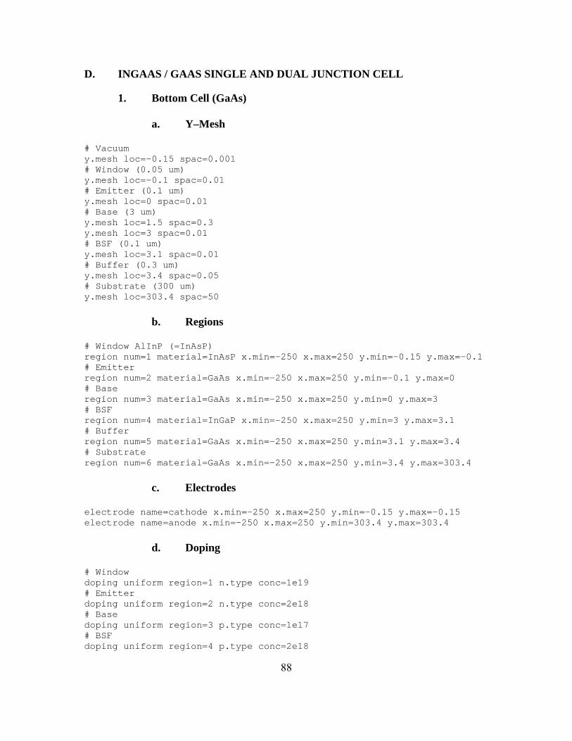
88
D. INGAAS / GAAS SINGLE AND DUAL JUNCTION CELL
1. Bottom Cell (GaAs)
a. Y–Mesh
# Vacuum y.mesh loc=-0.15 spac=0.001 # Window (0.05 um) y.mesh loc=-0.1 spac=0.01 # Emitter (0.1 um) y.mesh loc=0 spac=0.01 # Base (3 um) y.mesh loc=1.5 spac=0.3 y.mesh loc=3 spac=0.01 # BSF (0.1 um) y.mesh loc=3.1 spac=0.01 # Buffer (0.3 um) y.mesh loc=3.4 spac=0.05 # Substrate (300 um) y.mesh loc=303.4 spac=50
b. Regions
# Window AlInP (=InAsP) region num=1 material=InAsP x.min=-250 x.max=250 y.min=-0.15 y.max=-0.1 # Emitter region num=2 material=GaAs x.min=-250 x.max=250 y.min=-0.1 y.max=0 # Base region num=3 material=GaAs x.min=-250 x.max=250 y.min=0 y.max=3 # BSF region num=4 material=InGaP x.min=-250 x.max=250 y.min=3 y.max=3.1 # Buffer region num=5 material=GaAs x.min=-250 x.max=250 y.min=3.1 y.max=3.4 # Substrate region num=6 material=GaAs x.min=-250 x.max=250 y.min=3.4 y.max=303.4
c. Electrodes
electrode name=cathode x.min=-250 x.max=250 y.min=-0.15 y.max=-0.15 electrode name=anode x.min=-250 x.max=250 y.min=303.4 y.max=303.4
d. Doping
# Window doping uniform region=1 n.type conc=1e19 # Emitter doping uniform region=2 n.type conc=2e18 # Base doping uniform region=3 p.type conc=1e17 # BSF doping uniform region=4 p.type conc=2e18

89
# Buffer doping uniform region=5 p.type conc=7e18 # Substrate doping uniform region=6 p.type conc=1e19
e. Solving method newton maxtraps=10 itlimit=100 climit=1 dvmax=0.05 solve initial solve b1=0.9 log outf=multiIV.log solve vanode=0.0 name=anode vstep=0.025 vfinal=2.7 extract init infile="multiIV.log" extract name="Jsc" y.val from curve(v."anode", i."anode") where
x.val=0.0 extract name="Voc" x.val from curve(v."anode", i."anode") where
y.val=0.0
2. Top Cell (InGaP)
a. Y–Mesh
# Vacuum y.mesh loc=-0.87 spac=0.003 # Window (0.03 um) y.mesh loc=-0.84 spac=0.003 # Emitter (0.05 um) y.mesh loc=-0.79 spac=0.003 # Base (0.55 um) y.mesh loc=-0.5 spac=0.1 y.mesh loc=-0.24 spac=0.003 # BSF (0.03 um) y.mesh loc=-0.21 spac=0.003 # Buffer (0.03 um) y.mesh loc=-0.18 spac=0.002
b. Regions
# Window AlInP (=InAsP) region num=1 material=InAsP x.min=-250 x.max=250 y.min=-0.87 y.max=-0.84 # Emitter region num=2 material=InGaP x.min=-250 x.max=250 y.min=-0.84 y.max=-0.79 # Base region num=3 material=InGaP x.min=-250 x.max=250 y.min=-0.79 y.max=-0.24 # BSF region num=4 material=InGaP x.min=-250 x.max=250 y.min=-0.24 y.max=-0.21

90
# Buffer AlInP (=InAsP) region num=5 material=InAsP x.min=-250 x.max=250 y.min=-0.21 y.max=-0.18
c. Electrodes
electrode name=cathode x.min=-250 x.max=250 y.min=-0.87 y.max=-0.87 electrode name=anode x.min=-250 x.max=250 y.min=-0.18 y.max=-0.18
d. Doping
# Window doping uniform region=1 n.type conc=1.95e18 # Emitter doping uniform region=2 n.type conc=2e18 # Base doping uniform region=3 p.type conc=1.5e17 # BSF doping uniform region=4 p.type conc=2e18 # Buffer doping uniform region=5 p.type conc=0.95e18
e. Solving
(1) ISC and VOC method newton maxtraps=10 itlimit=100 climit=1 dvmax=0.05 solve initial solve b1=0.9 log outf=multiIV.log solve vanode=0.0 name=anode vstep=0.025 vfinal=2.7 extract init infile="multiIV.log" extract name="Jsc" y.val from curve(v."anode", i."anode") where
x.val=0.0 extract name="Voc" x.val from curve(v."anode", i."anode") where
y.val=0.0
3. Stacked Cell
a. Y–Mesh
# Vacuum y.mesh loc=-0.87 spac=0.003 # Window (0.03 um) y.mesh loc=-0.84 spac=0.003 # Emitter (0.05 um) y.mesh loc=-0.79 spac=0.003 # Base (0.55 um) y.mesh loc=-0.5 spac=0.1 y.mesh loc=-0.24 spac=0.003

91
# BSF (0.03 um) y.mesh loc=-0.21 spac=0.003 # Buffer (0.03 um) y.mesh loc=-0.18 spac=0.002 # Vacuum (0.015 um) y.mesh loc=-0.165 spac=0.002 # Vacuum (0.015 um) y.mesh loc=-0.15 spac=0.001 # Window (0.05 um) y.mesh loc=-0.1 spac=0.01 # Emitter (0.1 um) y.mesh loc=0 spac=0.01 # Base (3 um) y.mesh loc=1.5 spac=0.3 y.mesh loc=3 spac=0.01 # BSF (0.1 um) y.mesh loc=3.1 spac=0.01 # Buffer (0.3 um) y.mesh loc=3.4 spac=0.05 # Substrate (300 um) y.mesh loc=303.4 spac=50
b. Regions
# Window AlInP (=InAsP) region num=1 material=InAsP x.min=-250 x.max=250 y.min=-0.87 y.max=-0.84 # Emitter region num=2 material=InGaP x.min=-250 x.max=250 y.min=-0.84 y.max=-0.79 # Base region num=3 material=InGaP x.min=-250 x.max=250 y.min=-0.79 y.max=-0.24 # BSF region num=4 material=InGaP x.min=-250 x.max=250 y.min=-0.24 y.max=-0.21 # Buffer AlInP (=InAsP) region num=5 material=InAsP x.min=-250 x.max=250 y.min=-0.21 y.max=-0.18 # Vacuum region num=6 material=Vacuum x.min=-250 x.max=250 y.min=-0.18
y.max=-0.165 region num=7 material=Vacuum x.min=-250 x.max=250 y.min=-0.165
y.max=-0.15 # Window AlInP (=InAsP) region num=8 material=InAsP x.min=-250 x.max=250 y.min=-0.15
y.max=-0.1 # Emitter region num=9 material=GaAs x.min=-250 x.max=250 y.min=-0.1 y.max=0 # Base region num=10 material=GaAs x.min=-250 x.max=250 y.min=0 y.max=3 # BSF region num=11 material=InGaP x.min=-250 x.max=250 y.min=3 y.max=3.1 # Buffer region num=12 material=GaAs x.min=-250 x.max=250 y.min=3.1 y.max=3.4

92
# Substrate region num=13 material=GaAs x.min=-250 x.max=250 y.min=3.4 y.max=303.4
c. Electrodes
electrode name=cathode x.min=-250 x.max=250 y.min=-0.87 y.max=-0.87 electrode name=cc x.min=-250 x.max=250 y.min=-0.18 y.max=-0.18 electrode name=ee x.min=-250 x.max=250 y.min=-0.15 y.max=-0.15 electrode name=anode x.min=-250 x.max=250 y.min=303.4 y.max=303.4
d. Doping
# Window doping uniform region=1 n.type conc=1.95e18 # Emitter doping uniform region=2 n.type conc=2e18 # Base doping uniform region=3 p.type conc=1.5e17 # BSF doping uniform region=4 p.type conc=2e18 # Buffer doping uniform region=5 p.type conc=0.95e18 # Window doping uniform region=8 n.type conc=1e19 # Emitter doping uniform region=9 n.type conc=2e18 # Base doping uniform region=10 p.type conc=1e17 # BSF doping uniform region=11 p.type conc=2e18 # Buffer doping uniform region=12 p.type conc=7e18 # Substrate doping uniform region=13 p.type conc=1e19
e. Solving
method newton maxtraps=10 itlimit=100 climit=1 dvmax=0.05 solve initial solve b1=0.9 log outf=multiIV.log solve vanode=0.0 name=anode vstep=0.025 vfinal=2.7 extract init infile="multiIV.log" extract name="Jsc" y.val from curve(v."anode", i."anode") where x.val=0.0 extract name="Voc" x.val from curve(v."anode", i."anode") where y.val=0.0

93
4. Tunnel Junction
a. Y–Mesh
y.mesh loc=-0.18 spac=0.002 # Tunnel emitter (0.015 um) y.mesh loc=-0.165 spac=0.002 # Tunnel base (0.015 um) y.mesh loc=-0.15 spac=0.001
b. Regions
region num=1 material=InGaP x.min=-250 x.max=250 y.min=-0.18 y.max=-0.165 region num=2 material=InGaP x.min=-250 x.max=250 y.min=-0.165 y.max=-0.15
c. Electrodes
electrode name=cathode x.min=-250 x.max=250 y.min=-0.18 y.max=-0.18 electrode name=anode x.min=-250 x.max=250 y.min=-0.15 y.max=-0.15
d. Doping
doping uniform region=1 p.type conc=8e18 doping uniform region=2 n.type conc=1e19
e. QT Mesh qtx.mesh loc=-250 spac=50 qtx.mesh loc=0 spac=10 qtx.mesh loc=250 spac=50 qty.mesh loc==-0.165 spac=.001 qty.mesh loc=-0.1575 spac=.0005 qty.mesh loc=-0.15 spac=.001
f. Solving
method newton maxtraps=10 itlimit=100 climit=1 dvmax=0.05 solve initial solve b1=0.9 log outf=multiIV.log solve vanode=0.0 name=anode vstep=0.025 vfinal=2.7 extract init infile="multiIV.log" extract name="Jsc" y.val from curve(v."anode", i."anode") where x.val=0.0 extract name="Voc" x.val from curve(v."anode", i."anode") where
y.val=0.0

94
5. MJ Cell
a. Y–Mesh
# Vacuum y.mesh loc=-0.87 spac=0.003 # Window (0.03 um) y.mesh loc=-0.84 spac=0.003 # Emitter (0.05 um) y.mesh loc=-0.79 spac=0.003 # Base (0.55 um) y.mesh loc=-0.5 spac=0.1 y.mesh loc=-0.24 spac=0.003 # BSF (0.03 um) y.mesh loc=-0.21 spac=0.003 # Buffer (0.03 um) y.mesh loc=-0.18 spac=0.002 # Tunnel emitter (0.015 um) y.mesh loc=-0.165 spac=0.002 # Tunnel base (0.015 um) y.mesh loc=-0.15 spac=0.001 # Window (0.05 um) y.mesh loc=-0.1 spac=0.01 # Emitter (0.1 um) y.mesh loc=0 spac=0.01 # Base (3 um) y.mesh loc=1.5 spac=0.3 y.mesh loc=3 spac=0.01 # BSF (0.1 um) y.mesh loc=3.1 spac=0.01 # Buffer (0.3 um) y.mesh loc=3.4 spac=0.05 # Substrate (300 um) y.mesh loc=303.4 spac=50
b. Regions
# Window AlInP (=InAsP) region num=1 material=InAsP x.min=-250 x.max=250 y.min=-0.87 y.max=-0.84 # Emitter region num=2 material=InGaP x.min=-250 x.max=250 y.min=-0.84 y.max=-0.79 # Base region num=3 material=InGaP x.min=-250 x.max=250 y.min=-0.79 y.max=-0.24 # BSF region num=4 material=InGaP x.min=-250 x.max=250 y.min=-0.24 y.max=-0.21 # Buffer AlInP (=InAsP) region num=5 material=InAsP x.min=-250 x.max=250 y.min=-0.21 y.max=-0.18 # Tunnel emitter

95
region num=6 material=InGaP x.min=-250 x.max=250 y.min=-0.18 y.max=-0.165
# Tunnel base region num=7 material=InGaP x.min=-250 x.max=250 y.min=-0.165
y.max=-0.15 # Window AlInP (=InAsP) region num=8 material=InAsP x.min=-250 x.max=250 y.min=-0.15 y.max=-0.1 # Emitter region num=9 material=GaAs x.min=-250 x.max=250 y.min=-0.1 y.max=0 # Base region num=10 material=GaAs x.min=-250 x.max=250 y.min=0 y.max=3 # BSF region num=11 material=InGaP x.min=-250 x.max=250 y.min=3 y.max=3.1 # Buffer region num=12 material=GaAs x.min=-250 x.max=250 y.min=3.1 y.max=3.4 # Substrate region num=13 material=GaAs x.min=-250 x.max=250 y.min=3.4 y.max=303.4
c. Electrodes
electrode name=cathode x.min=-250 x.max=250 y.min=-0.87 y.max=-0.87 electrode name=anode x.min=-250 x.max=250 y.min=303.4 y.max=303.4
d. Doping
# Window doping uniform region=1 n.type conc=1.95e18 # Emitter doping uniform region=2 n.type conc=2e18 # Base doping uniform region=3 p.type conc=1.5e17 # BSF doping uniform region=4 p.type conc=2e18 # Buffer doping uniform region=5 p.type conc=0.95e18 # Tunnel doping uniform region=6 p.type conc=8e18 # Tunnel doping uniform region=7 n.type conc=1e19 # Window doping uniform region=8 n.type conc=1e19 # Emitter doping uniform region=9 n.type conc=2e18 # Base doping uniform region=10 p.type conc=1e17 # BSF doping uniform region=11 p.type conc=2e18 # Buffer doping uniform region=12 p.type conc=7e18 # Substrate doping uniform region=13 p.type conc=1e19
e. Solving

96
method newton maxtraps=10 itlimit=100 climit=1 dvmax=0.05 solve initial solve b1=0.9 log outf=multiIV.log solve vanode=0.0 name=anode vstep=0.025 vfinal=2.7 extract init infile="multiIV.log" extract name="Jsc" y.val from curve(v."anode", i."anode") where
x.val=0.0 extract name="Voc" x.val from curve(v."anode", i."anode") where
y.val=0.0

97
LIST OF REFERENCES
[1] Renewable Resource Data Center (www.rredc.nrel.gov). Last accessed on August 10, 2008.
[2] P. Michalopoulous, “A Novel Approach for the Development and Optimization of State-of-the-Art Photovoltaic Devices Using Silvaco,” Master’s Thesis, Naval Postgraduate School, Monterey, California, 2002.
[3] T Agui, T. Takamoto, E. Ikeda, and H. Kurita, “High-efficient dual-junction InGaP/GaAs solar cells with improved tunnel interconnectt,” Indium Phosphide and Related Materials, 1998 International Conference on, pp 203-206, 1998.
[4] S. M. Sze, Semiconductor Devices, 2nd edition, John Wiley & Sons, Inc, 2001.
[5] R. F. Pierret, Semiconductor Device Fundamentals, Addison-Wesley Publishing Company, Inc., 1996.
[6] Oklahoma State University Solid State/Chemistry Website (www.okstate.edu/jgelder/solstate.html). Last accessed on July 2, 2008.
[7] S. M. Sze, Physics of Semiconductor Devices, 2nd edition, John Wiley & Sons, Inc, 1981.
[8] D. A. Fraser, The Physics of Semiconductor Devices, Clarendon Press – Oxford, 1986.
[9] D. A. Neamen, Semiconductor Physics and Devices, McGraw-Hill companies, Inc, 2003.
[10] SILVACO International website (www.silvaco.com). Last accessed on August 15, 2008.
[11] S. M. Sze, Modern Semiconductor Device Physics, John Wiley & Sons, Inc, 1998.
[12] A. D. Bates, “Novel Optimizatoin Techniques for Multijunction Solar Cell Design Using Silvaco Atlas,” Master’s Thesis, Naval Postgraduate School, Monterey, California, 2005.
[13] S. Michael and J. Lavery, “Multi-Junctoin Photovoltaic model Optimizatoins for Space and Solar Concentrator Applications,” Proceedings of the 23rd European Photovoltaic Solar Energy Conference, Valencia, Spain, September 1-5, 2008.
[14] M. Shur, Physics of Semiconductor Devices, Prentice–Hall, Inc, 1990.
[15] R. P. Feynman, The Feynman Lectures on Physics, Volume I, Addison-Wesley Publishing Company, 1989.
[16] Georgia State University hyperphysics website (http://hyperphysics.phy-astr.gsu.edu). Last accessed on May 28, 2008.

98
[17] T. Takamoto, I. Kurita, and H. Ohmori, “High efficiency InGaP solar cells for InGaP/GaAs tandem cell application,” Photovoltaic Energy Conversion in 1994, Volume: 2, pp. 1729–1732, 1994.
[18] B. Cavicchi, D. Krut, D. Lillington, S. Kurtz, and J. Olson, “The design and evaluation of dual-junction GaInP/sub 2//GaAs solar cells for space applications,” Photovoltaic Specialists Conference in 1991, pp. 63-67, vol. 1, 1991.
[19] D. Lillington, H. Cotal, J. Ermer, D. Friedman, T. Moriarty, and A. Duda, “32.3% efficient triple junction GaInP/sub 2//GaAs/Ge concentrator solar cells,” Energy Conversion Engineering Conference and Exhibit in 2000, (IECEC) 35th Intersociety, Volume: 1 , 2000, pp. 516 -521.
[20] J. Granata, J. Ermer, P. Hebert, M. Haddad, R. King, D. Krut , J. Lovelady, M. Gillanders, N. Karam, and B. Cavicchi, “Triple-junction GaInP/GaAs/Ge solar cells-production status, qualification results and operational benefits,” Photovoltaic Specialists Conference in 2000, pp. 1181 -1184.
[21] R. King, N. Karam, J. Ermer, N. Haddad, P. Colter, T. Isshiki, H. Yoon, H. Cotal, D. Josli, D. Krut, R. Sudharsanan, K.Edmondson, B. Cavicchi, and D. Lillington, “Next-generation, high-efficiency III-V multijunction solar cells,” Photovoltaic Specialists Conference in 2000, Conference Record of the Twenty-Eighth IEEE, 2000, pp 998-1001.
[22] Department of Energy (www.doe.gov). Last accessed on June 24, 2008.
[23] J. Slotboom, “The PN Product in Silicon,” Solid State Electronics 20 (1977): 279-283.
[24] I. Vurgaftman, J. Meyer, and L. Ram–Mohan, “Band parameters for III–V compound semiconductors and their alloys,” Applied Physics Review, Journal of Applied Physics, vol. 89, number 11, June 1, 2001, pp. 5815–5875.
[25] P. Sharps, J. Hills, and H. Hou, “AlGaAs/InGaAlP TUNNEL JUNCTIONS for MULTI-JUNCTION SOLAR CELLS,” EMCORE Photovoltaics. IEEE 2000.

99
INITIAL DISTRIBUTION LIST
1. Defense Technical Information Center Ft. Belvoir, Virginia
2. Dudley Knox Library Naval Postgraduate School Monterey, California
3. Chairman, Department of Electrical and Computer Engineering Naval Postgraduate School Monterey, California
4. Dr. Sherif Michael, Code EC/Mi Department of Electrical and Computer Engineering Monterey, California
5. Dr. Todd Weatherford, Code EC/Wt Department of Electrical and Computer Engineering Monterey, California