eeedidieee - dtic
TRANSCRIPT
AD-A116 162 WASHINGTON UNIV SEATTLE DEPT OF ELECTRICAL ENGINEERING F/6 20/12CONTROL OF GAAS MICROWAVE SCHOTTKY DIODE ELECTRICAL CHARACTERIS-ETC(UlMAY 82 S J TENS, R E GOLDWASSER N00014'79-C-060
UNCLASSIFIED TR-ONR-82-1 w
SLEEEEEEEEEEI
'EEEDIDIEEE1Eu 2hE~E

i c IIU-L 111112.51 1l 0 111112
_________IIIII o
MIiiCI.25 ROLU.4 11 11.6
MICROCOPY RESOLUTION TEST CHARTNA110NAt U0,1 ,, !,'Nt A

r-4
r04
rN4ot
inMICC


WASHINGTONUNIVERSITYIN ST LOUIS
CONTROL OF GaAs MICROWAVE SCHOTTKY DIODEELECTRICAL CHARACTERISTICS BY CONTACT
GEOMETRY: THE GAP DIODE
S.J.J. TENGR.E. GOLDWASSERF.J. ROSENBAUM
Department of Electrical EngineeringWashington UniversitySt. Louis, Mo. 63130
MAY 1982 .
TECHNICAL REPORT ONR-82-1
Office of Naval ResearchArlington, VA 22217
Reproduction, in whole or in part, is permitted for any purpose of the U.S. Government
Contract NO0014-79-C-840
Contract Authority* NR SRO-004
Approved for public release; distribution unlimited.

TABLE OF CONTENTS
No. Page
1. Introduction .............................................. 1
1.1 Metal-Semiconductor Schottky-Barrier ................. 2
1.2 Metal-Semiconductor Barrier Height ................... 3
1.3 Control of Barrier Height ............................ 6
1.3.1 Highly Electronegative Contacts ............... 61.3.2 Doping Variations Near the Contact ............ 7
1.3.2.1 Alloying ............................. 71.3.2.2 Ion Implantation ..................... 81.3.2.3 Ion Bombardment ...................... 8
1.3.3 Thin Interfacial Insulating Layers ............ 81.3.4 Edge Tunneling ........ ....................... 91.3.5 Gap-Controlled Low Barrier .................... 9
2. Gap-Controlled (Low Barrier) Schottky Diode ............... 11
2.1 Schottky-Barrier Model ............................... 11
2.2 Ohmic Contact to GaAs ................................ 16
2.3 Theory of Gap-Controlled Charge Transport ............ 18
2.3.1 Basic Characteristics ......................... 182.3.2 Current-Voltage Relationship .................. 24
2.3.2.1 Notched-type Gap Diode ............... 242.3.2.2 Planar-type Gap Diode ................ 29
3. Vapor-Phase Epitaxial Growth of GaAs ...................... 37
3.1 Description of Epitaxial Reactor ..................... 37
3.2 Source Saturation .................................... 40
3.3 Epitaxial Growth Procedure ... .............. 42
3.4 H S Dopant Incorporation ......... 44
3.5 Substrate Preparation ....... ... . " 45'J 'i fi0+. + t : c,
3.6 Material Evaluation...... ... 45
t~~~~~~ ... \i owall."
10.A v YCodes,, d/or

iv
TABLE OF CONTENTS(conti nued)T
No. Page
4. Device Fabrication .................................... 49
4.1 Device Construction............................... 49
4.2 Ohmic Contact Fabrication ......................... 49
4.3 Schottky-Barrier Fabrication....................... 52
4.4 Junction Formation................................ 55
4.5 GaAs Mesa Etch and S10 Insulation ................... 57
4.6 Diode Packaging .................................. 57
5. Experiment Results and Discussion....................... 62
5.1 Current-Voltage Characteristics ..................... 62
5.2 Diode Capacitance................................. 70
5.3 Temperature Dependence of the I-V Characteristics ... 72
5.4 Detector Characteristics .......................... 77
5.5 Mixer Characteristics............................. 80
6. Conclusions .......................................... 85
7. Acknowledgement....................................... 88
8. Bibliography ......................................... 89
LIST OF FIGURES
No. Page
1. Schematic representation of electric field andpotential resulting from surface states in theSchottky-barrier depletion region .................... 4
2. Experimental barrier heights for metal contacts ton-type Si, GaAs, GaP and CdS [4] ..................... 5
3. One-dimensional parabolic depletion layer potentialenergy barrier for an n-type semiconductor. Imageforce rounding of the barrier shape is neglected ..... 12
4. Schematic diagram of gap-controlled Schottky diode(a) notched type (b) planar-type .................. 19
5. Cross-sectional view of notched-type gap-controlledSchottky diode with applied bias voltage VA .......... 22
6. Calculated forward I-V characteristics of the notched-type Gap diode from Equation (2.19) as a function ofohmic gap width W .................................... 27
7. Calculated relationship between the turn-on voltage(at IA = 1 M), ohmic gap width W and semiconductorcarrier concentration ND of the notched-type Gapdiode .............................................. . 28
8. Calculated relationship between the turn-on voltage(at IA = I mA), ohmic gap width W and semiconductorchannel length Z of the notched-type Gap diode ....... 30
9. Cross-sectional view of planar-type gap-controlledSchottky diode with applied bias VA
a) voltage dependent depletion region modelb) semicircular depletion region model .......... 31
10. Schematic diagrams of a depletion approximation modelfor planar-type Gap diodes ........................... 35
11. Schematic of AsCZ3-Ga-H 2 vapor phase epitaxialsystem ....................................... 38
12. Temperature profile of the furnace. Curve (a) isused for the Ga-baking in H2 and saturation with Asof Ga source. Curve (b) is for the epitaxialgrowth ............................................... 39

vii
LIST OF FIGURES(continued)
No. Page
13. Doping density as a function of H2S flow rate ........ 46
14. Cross-section of planar-type gap-controlled GaAsSchottky-barrier diode ............................... 50
15. Carrier concentration versus depth for VPE grownlayer from Schottky barrier profile measurements ..... 51
16. Photograph of 1.5 pm photoresist grating pattern
on the GaAs epitaxial layer .......................... 53
17. Process used to fabricate planar-type gap diodes ..... 54
18. Photographs of 32 pm diameter. Photoresist dots onthe aluminum and AuGe/Ni lines ....................... 56
19. Photograph of unalloyed AZ/AuGe/Ni stripe dots on
GaAs surface after metal etching ..................... 58
20. Completed Gap diodes on a scribed GaAs chip .......... 59
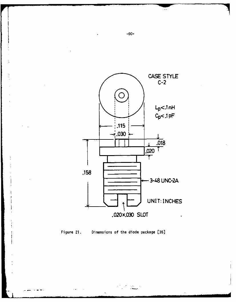
21. Dimensions of the diode package [35] ................. 60
22. Photograph of a GaAs Gap diode chip mounted in aC-2 package, bonded with 1 mil Au wires .............. 61
23. Photographs of various measured low-frequency I-V
characteristics of the planar-type diodes as ohmicgap width, W, is gradually increased from zero tomore than two depletion widths ....................... 63
24. Photographs of I-V characteristics measured fromtwo typical low-leakage packaged planar-typeGap diodes (Gap diodes U-2, U-5) ..................... 64
25. Photographs of I-V characteristics measured from twowide gap width packaged planar-type Gap diodes(Gap diodes T-9, E-8-B) .............................. 66
26. Photographs of I-V characteristics of a packaged
planar-type Gap diode with two different currentand voltage scales (Gap diode U-4) ................... 67
'7

vii
LIST OF FIGURES(continued)
No. Page
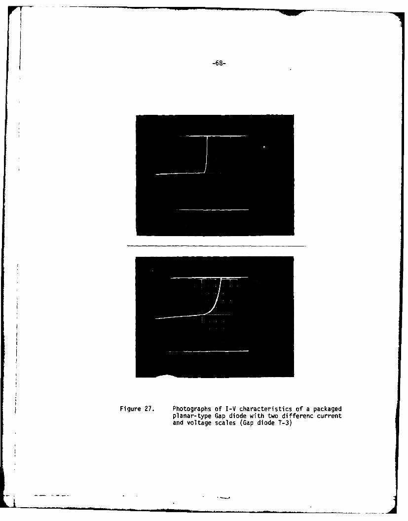
27. Photographs of I-V characteristics of a packagedplanar-type Gap diode with two different currentand voltage scales (Gap diode T-3) ................... 68
28. Representative I-V characteristics of a low-leakageGap diode and a pure At Schottky diode of thesame size ............................................ 69
29. Measures forward I-V characteristics of several Gapdiodes and a pure AZ Schottky diode .................. 71
30. Photograph of the temperature dependence of theforward I-V characteristics of a AZ Schottky diodemeasured at four different temperatures .............. 73
31. Photograph of the temperature dependence of I-Vcharacteristics for a Gap diode ...................... 75
32. Forward I-V characteristics of a pure Schottkydiode (UP-5) and a Gap diode (U-2) measured at210C and 100C respectively .......................... 76
33. Photograph of temperature dependence of I-Vcharacteristics of (a) a point contact diode(IN23C) (b) a Gap diode at 220C, 800C and 920C ...... 78
34. Open-circuit voltage output versus incident RFpower for Gap diode (V-10), point contact diode(IN23C) and Schottky diode (UP-4) at 10.565 GHz ...... 79
35. Open-circuit voltage output versus incident RF
power of a Gap diode (V-10) .......................... 81
36. Single-ended mixer conversion loss measuring setup ... 82
37. Single-ended mixer conversion loss versus localoscillator power for three different Gap diodes(at 10 GHz, 20 MHz IF). The ohmic gap widthincreases from diode U-3 to diode U-7 ................ 84

CONTROL OF GaAs MICROWAVE SCHOTTKY DIODE ELECTRICAL
CHARACTERISTICS BY CONTACT GEOMETRY: THE GAP DIODE
1. INTRODUCTION
Point-contact diodes have been used for many years in mixer and
detector applications at microwave frequencies. They are relatively
unsophisticated devices consisting of a metal whisker making pressure
contact with a semiconductor. In the early 1960's, Schottky-barrier
diodes were introduced for similar applications. Schottky diodes
have superior noise figure, especially at low IF (Doppler) frequen-
cies, higher burn-out power and better mechanical environmental
reliability compared to equivalent point contact diodes [l,2]*.
The GaAs Schottky-barrier diode is preferred to Schottky diodes
using other materials owing to its high electron mobility which re-
sults in better high frequency performance. Also, both higher and
lower temperature operation can be obtained with GaAs owing to its
higher energy gap. GaAs Schottky diodes have been shown to have
low noise [3); however, reported barrier heights have been
* The numbers in parentheses in the text indicate references in theBibliography.

-2-
substantially higher than point contact silicon diodes and greater
than most silicon Schottky diodes. Barrier heights are related to
minimum local oscillator power, the higher barrier devices requiring
larger local oscillator power. Therefore, in microwave systems having
limited local oscillator power, a low barrier height device is
desirable [2,3].
In this report, a new contact technique, which employs conven-
tional Schottky metal contacts separated by ohmic contact gaps to
obtain low diode turn-on voltage, is presented. The characteristics
of the device made with this new contact configuration, GaAs vapor
phase epitaxial growth, and microfabrication technology for the device,
together with some microwave measurements, are also described. A
discussion of the physics and metallurgy of the metal-semiconductor
contact is also presented.
1.1 METAL-SEMICONDUCTOR SCHOTTKY-BARRIER
Metal-semiconductor Schottky-barrier contacts are used in many
semiconductor devices, including switches, rectifiers, varactors,
IMPATTs, mixer and detector diodes, parametric amplifiers, field
effect transistors (MESFETs), and photodetectors. Most of these appli-
cations are based on the use of the electron transport properties of
the particular metal-semiconductor barrier considered. For each
device the design factors depend on the application and may include
the metal barrier, semiconductor material, device geometry, passi-
vation, and device packaging.
It is important to study the operation and to optimize the
current-voltage characteristic of metal-semiconductor contacts.
L "'
I-3-
Study of such contacts has been pursued since 1938 when Schottky
postulated that a potential barrier could arise from a metal-semicon-
ductor interface without the presence of a chemical layer.
1.2 METAL-SEMICONDUCTOR BARRIER HEIGHT
The simple theory of metal-semiconductor contacts [4,5] predicts
that the work function of the metal should be a design parameter in
controlling the barrier height. Unfortunately, for semiconductors
which possess a high surface state density, the barrier height,
becomes insensitive to work function. It was first proposed by
Bardeen [6) that the influence of a high density of surface states
pins the Fermi level at the interface, thus fixing the barrier height.
It is experimentally observed that the barrier height for covalent
semiconductors is essentially independent of the metal used [7].
Like the group IV semiconductors Si and Ge, GaAs and most of the other
III-V compound semiconductors are highly covalent. For highly ionic
materials such as most of the II-VI compound semiconductors (e.g. ZnS
and ZnO) and the transition-metal oxides, the barrier height is
strongly dependent on the work function of the metal [7].
The electric field and potential resulting from surface states
in the Schottky-barrier depletion region is shown in Figure 1.
Figure 2 shows experimental data on barrier height, *B' for a range
of metals on n-type Si, GaAs, GaP and CdS [4]. The ability to vary
OB for different applications is important for device optimization.
For example, in a mixer diode the capability of the device to handle
low signal levels without d.c. bias requires low turn-on voltage.
Consequently, a mixer or detector diode requires a low barrier
.- * ~s.*m

-4-
SCHOTTKY FIELD
METAL SEMICONDUCTOR
SURFACE STATE FIELDAND IMAGE FIELD
t !SURFACE#B STA TES
ttMETAL SEMICONDUCTOR
Figure 1. Schematic representation of electric field andpotential resulting from surface states in theSchottky-barrier depletion region
'- -

-5-
2.0
Si SGOP sAGo Ass 0
Ud S 0 GoP
-1.0 G Sao-
o ,b. .,i ,0;0 d
3.0 4.0 5.0 6.0q (ev)
Figure 2. Experimental barrier heights for metal contacts to
n-type Si, GaAs, GaP and CdS [4]

-6-
height that will yield a low forward voltage drop. For this reason
the point contact diode has traditionally been preferred to the
evaporated Schottky diode. A mixer also requires low series
resistance for high conversion efficiency. Therefore GaAs is pre-
ferred to silicon because the high mobility of the undepleted material
is more important than its high contact potential, about 0.8 ev.
1.3 CONTROL OF BARRIER HEIGHT
There are several techniques available for varying the effective
barrier height of metal contacts to materials with high surface
state densities. An introduction of these techniques is made in
the following sections. The barrier height may be used as a design
parameter for Schottky diodes with the aid of barrier variation
techniques.
1.3.1 Highly Electronegative Contacts [8]
It is seen in Figure 1 that the insensitivity of the barrier
height to the electronegativity of the contact metal in semicon-
ductors with high surface state densities prevents the use of in-
trinsic barrier height as a control parameter. Attempts to over-
come this problem for II-VI and III-V compound semiconductors have
led to some developments in the use of highly electronegative
metallic compounds, rather than elemental metal materials, such as
polymeric sulfur nitride (SN) and the mercury chalcogenides toxextend the available range of Schottky barrier heights [8]. These
metallic compounds produce higher barriers to n-type semiconductors
and lower barriers to p-type semiconductors than do the elemental
metals. For example, studies of the use of the (SN)x compounds on

-7-
n-type GaAs and InP indicate that the Schottky-barrier heights are
increased by 0.1 ev and 0.3 ev respectively, compared to those obtained
with Au [8].
1.3.2 Doping Variations Near the Contact [9]
As the carrier concentration of a semiconductor is increased,
the depletion width under the Schottky contact decreases and the
surface field increases. With the increased doping, the dominant
transport mechanism across the barrier can change from thermionic
emission to thermionic field emission [4]. Therefore, the effective
barrier height of a Schottky-barrier having a highly doped surface
layer can be controlled over a wide range. Reduction of barrier
height is effected by increasing the surface field and encouraging
quantum-mechanical tunneling through the barrier; increase of
barrier height occurs when the surface field is reversed. In
practice, the semiconductor can be made degenerate which results
in an ohmic contact.
1.3.2.1 Alloying [10,11,12]
A simple way to achieve local variation in doping is to alloy
the contact. The dopant is diffused into the semiconductor. For
materials such as GaAs and InP the contact metal is usually a mix-
ture of elements such as AuGe or AgSn, where Ge or Sn is used as a
dopant. Also a single-component metal Schottky-barrier can be
heated to produce interdiffusion at the interface. For example, the
heating of a Au/GaAs barrier to 4500C results in a reduction of the
effective barrier height from 0.95 to 0.48 ev [12).

-8-
The basis for either alloying technology is empirical and not
very reproducible. One of the problems of the alloying process
described above is nonuniformity, due to the incomplete removal of
residual surface oxides prior to the evaporation of the metal contact.
1.3.2.2 Ion Implantation [13,14]
Ion implantation is a technique that can be more controllable
than the means described above for modifying the effective barrier
height, because the depth and surface density of the implanted
impurity can be controlled accurately by adjusting the energy of the
implant. The implantation of donors into n-type material, followed
by the usual annealing procedure to reduce the damage and activate
the dopants, can be used to reduce the effective barrier height [14].
1.3.2.3 Ion Bombardment [15]
Semiconductor defects resulting from ion bombardment can be
used instead of implanted dopants, to change the effective barrier
height. Consider a metal-semiconductor junction. If deep levels
are introduced into the semiconductor near the interface, the sur-
face state density will increase and the valence hand will bend
downward at the interface as shown in Figure 1.
1.3.3 Thin Interfacial Insulating Layers [16,17,18]
Thin interfacial oxide films can have a strong effect on
terminal I-V and C-V characteristics. Published experimental
results on Si, GaAs and InP reveal that the use of interfacial
layers is beginning to prove a valuable addition to Schottky
barrier technology.
iI

-9-
1.3.4 Edge Tunneling [19]
As the diameter of a planar Schottky-barrier device is reduced,
the depletion region at the circumference of the metal contact nar-
rows, and the thermionic field emission (tunnelling) current component
increases, resulting in a decrease in the effective barrier height.
This high edge field tunnelling phenomenon is the reason why point
contact diodes have a low turn-on voltage.
1.3.5 Gap-Controlled Low Barrier
When the applied voltage varies, the depth of the high resis-
tivity depletion region of the Schottky-barrier also varies. If ohmic
contact gaps are opened in the Schottky-barrier, then the current-
voltage characteristic of the resulting device can be modulated by
varying the configuration of the ohmic contact openings.
This report describes the investigation of this new barrier
lowering technique. GaAs Schottky-barrier diodes, combined with
AuGe/Ni ohmic contacts, have been fabricated and used to detect
signals at microwave frequencies. Depending on the width of the ohmic
contact gaps, the experimental diodes exhibit either high efficiency
microwave detection or low turn-on Schottky-barrier mixers requiring
low RF local oscillator power comparable to that of point contact
diodes.
Chapter 2 describes the principle of operation of the Gap diode
and presents some approximate theory for the current-voltage rela-
tionship for two different types of Gap diodes. The design of a GaAs
epitaxial growth reactor and growth techniques are described in
Chapter 3, while Chapter 4 presents the technology used to fabricate
experimental GaAs Gap diodes. Device characteristics and RF per-
formance are reported in Chapter 5. Our results are summarized
and recommendations for future work are presented in Chapter 6.
* I
I ..... .. . .. . . . . . 1 ' ,

-11-
2. GAP-CONTROLLED LOW-BARRIER SCHOTTKY DIODE
In this chapter the physics of the Schottky barrier junctions
is reviewed and the principle of operation of the Gap diode is
explored. Prediction of the device I-V characteristics are
developed.
2.1 SCHOTTKY-BARRIER MODEL
Schottky's diffusion theory [20] in an intimate metal-semicon-
ductor contact postulates the existence of a space charge region
which gives rise to an electrostatic potential energy barrier.
The space charge region, which is depleted of mobile carriers, is
situated in the semiconductor adjacent to the metal layer. The
analytical description of the barrier yields the relationship
between the applied bias, barrier height, donor concentration
and energy band bending in the semiconductor. In the absence
of image force rounding and assuming that the ionized impuri-
ties are uniformly distributed in the semiconductor, the one-
dimensional parabolic potential energy barrier in the semicon-
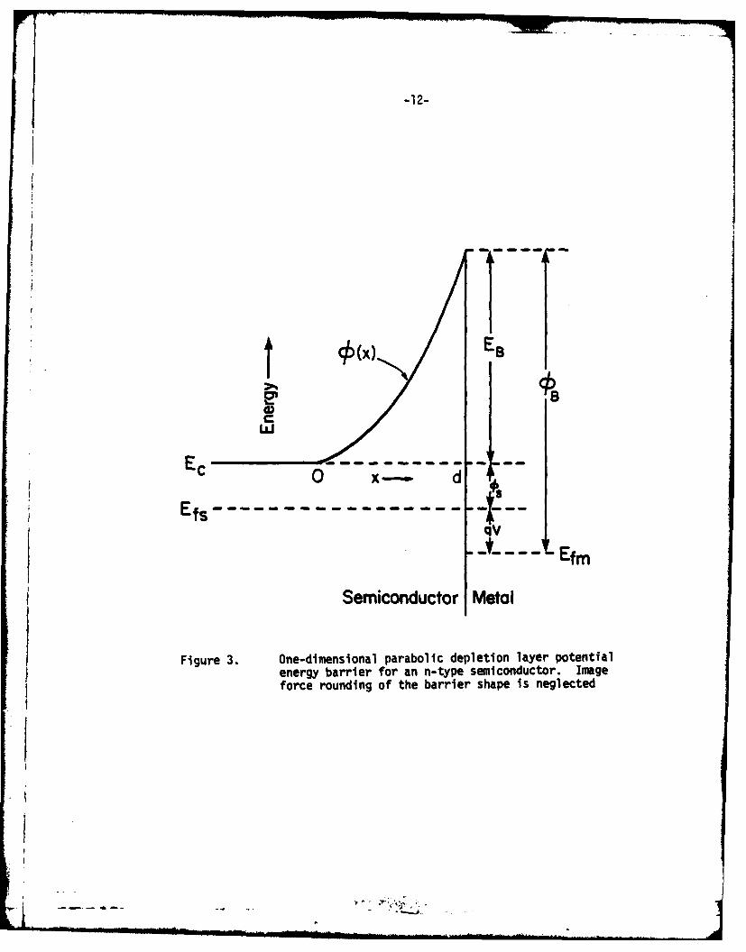
ductor depletion region, shown in Figure 3, is described by
q2NDX2
O(x) 2e (2.1)so0
for 0 < x < d
Here q is the electronic charge, ND is the ionized donor concentra-
tion, s is the static dielectric constant, and Eo the permittivity
-... - -R ,, .. . , -.... ......-- . .. . ----- -- =... . . ....... .. . .. "
-12-
fw Es
Ec 0S -x- - - - - - - - -- - - -- - - -
Semiconductor Metal
Figure 3. One-dimensional parabolic depletion layer potentialenergy barrier for an n-type semiconductor. Imageforce rounding of the barrier shape is neglected

-13-
of free space. The depletion layer width, d is related to the energy
band bending in the depletion region, EB, by
q2NDd2
EB = - s " qV 2E (2.2)
where OB is the metal-semiconductor barrier height, Os the position
of the semiconductor Fermi level relative to the conduction band
edge, and V the applied bias.
Depending on the difference of work function between the semi-
conductor and metal, three other configurations are possible: a
depletion layer barrier for p-type semiconductor, and accumulation
layers (ohwL :o)act) for n or p-type material.
For low-doped Schottky-barrier diodes, using Maxwell-Boltzmann
statistics to describe the distribution of carriers that can be
emitted over the barrier, one can relate the forward carrier flux
Jf and reverse carrier flux Jr by
if = Jr exp (a") (2.3)
where ir =A* T2 exp ( ) (2.4)*
Here, A is the Richardson constant of the semiconductor [21], K is
Boltzmann's constant and T the absolute temperature. The total
current density can be written as:

-14-
jJaf - ar =a [exp (k--V ) - I]
2 ('-q¢B
: A T2 exp (--kB) [exp (kV ) - 1] (2.5)
which represents ideal thermionic emission over the barrier. The
diode equation derived from the Schottky's diffusion theory [20]
yields a bias dependent pre-exponential term different from AT 2 .
In reality, the shape of the potential barrier is not parabolic
because charge carriers in the semiconductor are electrostatically
attracted towards the metal by an induced mirror image charge of
opposite sign in the metal. The image force effect changes the
potential distribution to
q 2ND X2 q2
*(x) =2e C 16edeo(d-x) (2.6)
where Ed is the relative dynamic dielectric constant of the semi-
conductor [22].
The lowering of the barrier due to the image effect is given by
(23]
Sq2EBND 4
2 2sd2o) (2.7)
Therefore, as the donor concentration, ND, of the semiconductor is
increased, the depletion width narrowing (d a ND'1/2) proceeds more1/4rapidly than the potential barrier lowering (A¢ a N and,
.. n

p. EN
-15-
consequently, the carrier transport is dominated by quantum-
mechanical tunneling rather than by themionic emission through
the barrier. Because of the image force effect, the actual
barrier height is OB - AO where AO is bias dependent (see Equations
(2.2) and (2.7).
For materials doped with ND < 017 cm-3 , thermionic emission
of carriers gives rise to current rectification in Schottky barriers.
There are two other modes of carrier transport over the Schottky
barrier that involve tunneling effects. As the impurity concen-
tration of the semiconductor is increased (ND l18 - 19 cm-3),
initially, the barrier becomes thin enough that thermally excited
carriers can tunnel through near the top of the barrier. This
mode of carrier transport is referred to as thermionic field
emission or thermally-assisted tunneling, which is temperature
dependent.
As the impurity concentration is increased even further
(ND> 10 19 cm'3), the barrier width becomes so thin that signifi-
cant numbers of carriers can tunnel through even at the base of
the barrier. This mode is called field emission tunneling and is
temperature independent. The mechanism of metal-semiconductor ohmic
contacts is based on this mode of carrier transport.
Because of the image force lowering, and the presence of
inevitable surface states and interfacial dielectric layers
between the metal and semiconductor, a dimensionless empirical
factor n is introduced in the diode equation in order to allow
L[ _. - .... j ! m ... . . .... . . . ... . . .
-16-
for deviation from ideality. The current, I, of the Schottky-barrier
is related to the applied voltage, V, by the expression
I = Is (exp( -) - 1] (2.8)
where is S' A** T2 qB (2.9)
I is the saturation current
S' is the area of the diode
The ideality factor, n, is a function of temperature, and is
determined from the slope of linear plots of ZnI against V. The
slope of the forward characteristic is measured for V >> 3nKTq
Is is determined by the extrapolation from higher forward bias
voltage to zero voltage of the tnI versus V plot.
2.2 OHMIC CONTACT TO GaAs [7,10,24,25,263
The most common method of making an ohmic contact is to place
a metal layer in contact with a semiconductor surface of very high
doping, to achieve field-emission dominated carrier transport so
that the potential barrier will appear almost transparent to the
carrier flow. There are many ways to make such a highly doped
surface layer such as alloy regrowth, diffusion of dopant con-
tained in the contact material, epitaxial regrowth, or ion
implantation.
For the alloy regrowth technique, the metal dissolves some of
the semiconductor during heating. Upon cooling the dissolved
-17-
semiconductor will regrow on the underlying crystal. The regrown
layer will contain a substantial concentration of the metal which
acts as a dopant (e.g. Au - n GaAs). If higher doping level and
lower alloying temperature are required it is often advantageous
to utilize another dopant impurity in addition to the contact
metal (e.g. Au-Ge-n GaAs).
The ohmic contact used for the fabrication of the Gap diode
in this report is the widely used Ni/Au-Ge/n-GaAs alloyed contact
[25,26]. The explanation for this ohmic behaviour is that the
diffused Ge atoms occupy Ga vacancies during alloying and form
a+ layer, sufficiently heavily doped to produce a linear
current-voltage characteristic at the contact interface. Ni plays
an active role in the contact formation. Wittmer, et al. [25]
have shown experimentally that during heat treatment the Ge
diffuses out of the Au into the Ni layer and forms stable compounds.
The Ni layer acts as a sink for Ge and the uniformity of the alloyed
layers depend on the ratio of the amount of the evaporated Ge to Ni.
From Auger electron spectroscopy (AES), it is known that the Ni does
not remain on top of the Au-Ge layer but it moves rapidly under the
Au-Ge layer before the Au-Ge melting point is reached [26]. The
reason for the improvement in surface uniformity due to the inclusion
of Ni is'that the presence of Ni at the GaAs surface greatly improves
the wetting of liquid Au-Ge to GaAs.
-18-
2.3 THEORY OF GAP-CONTROLLED CHARGE TRANSPORT
2.3.1 Basic Characteristics
In a conventional Schottky-barrier diode charge carriers must
surmount the potential barrier at the metal-semiconductor interface
to contribute to the current. An exponential relation between the
applied voltage and the current results. Another means of obtaining
a voltage controlled current is conductivity modulation, as for
example, in the Field Effect transistor. This process can be used
to make a diode whose performance will be markedly different from
that of the conventional Schottky-barrier diode.
Consider what happens if a gap is opened in the Schottky metal
on the surface of an n-type epitaxial layer, thus exposing the under-
laying n-layer. Now an ohmic metallization is applied to the entire
surface. This forms an ohmic contact to the n-layer and connects
it and the separated Schottky contacts in parallel.
Two types of Gap diodes are shown in Figures 4a and 4b, one
with the Schottky metal on the upper surface, the other with the
metal deposited into notches extending below the surface. The device
cpmprises an n-type layer grown epitaxially on a heavily doped n+
substrate with an ohmic contact fabricated on the substrate side of
the wafer. The diode consists of a conductive channel with an ohmic
contact on top, provided with two Schottky-barrier contacts acting as
gates to control the conductance of the conductive channel. Thus the
gap-controlled Schottky is basically an intrinsic-biased voltage-
controlled resistor whose resistance can be varied with the width of
'1

-19-
V SCHOTTKY
(a)A
OHOHMICONCONTAC
I CONTACT
Fiur 4 chmaicdagamo gp-onrlld chtkyDid
(a) nce taye ()panrt

-20-
the depleted space-charge region extending into the channel. Current
is transported predominantly by electrons only.
The potential distribution in the barrier layer of a metal-
n-type semiconductor can be calculated by solving Poisson's
equation, proceeding in the same manner as for the abrupt p-n junc-
tion. Under the abrupt junction approximation, the depletion width,
d, of the barrier layer can be expressed as
d = I o (Vo-V) (2.10)
where V is the diffusion potential or built-in voltage of the
metal-semiconductor junction, V the applied voltage, and ND the
donor concentration.
The space-charge density p of the semiconductor is
p = q(ND-n) (2.11)
where n is free electron concentration. Inside the depletion region,
p qND , x < d. In the neutral region the potential is constant,dV
that is -L-- 0, p=O, n=ND, x > d. This is the depletion approximation.
If the image force effect is included, the depletion width of
the semiconductor in thermal equilibrium may be written as [4]
d = T Bn + - V - q-) (2.12)
Lk ~ ~ ~ ~ ~ ~ q ....... . .... ... . ,, Nn +... V

-21-
where OBn is the metal-semiconductor barrier height and AO is the
image force barrier lowering. The term Earises from the con-
qtribution of mobile carriers to the electric field in the
depletion region.
In Figure 5, we illustrate the condition with an applied
bias V = VA. If a small positive voltage is applied to the
metal the depleted region separate and a current will be conducted
through the n-type channel between the ohmic contacts. No charge
flows in the depletion regions. As the voltage is increased, the
width of the undepleted channel grows and the channel conductance
increases. The I-V characteristic is not linear and is determined by
the structure of the diode. As the applied positive voltage is
further increased beyond the turn-on voltage of the Schottky-barrier,
another current component will arise due to charges flowing through
the Schottky-barriers. Thus the current of the diode consists of two
components:
I (Total current) = I, (current through the ohmic region)
+ 12 (current through the Schottky barrier) (2.13)
In the reverse-bias case, when negative voltage is applied to
the metal, the depletion width is increased. This restricts
current conduction through a smaller channel cross-sectional
area. Thus the channel resistance is increased. As the
reverse bias is further increased, the enlarged depletion
regions will eventually touch in the channel near the substrate
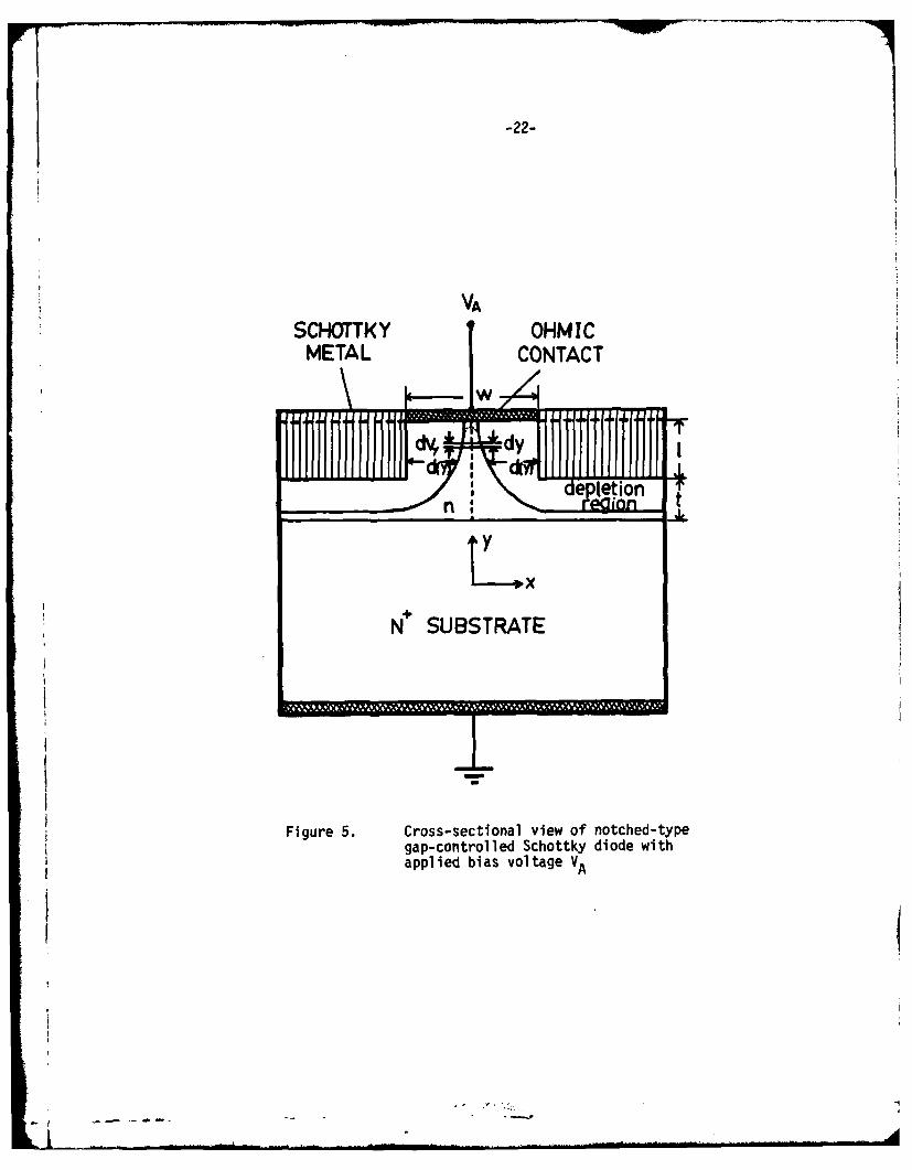
-22-
VA
SCHOTTKY OHMICMETAL CONTACT
W 74dyF
o 4o ,xI
N SUBSTRATE
Figure 5. Cross-sectional view of notched-typegap-controlled Schottky diode withapplied bias voltage VA
-23-
side. This happens when the ohmic gap width W = 2d. Using
Equation (2.10), the corresponding applied voltage may be expressed as
qNDW2Vsat =0s Vo (2.14)
At this saturation voltage, Vsat' the channel is completely depleted
and normally does not conduct because there are very few carriers
in it. However, similar to the field-effect transistor, a
current will still be conducted through the diode by drift of
carriers from the ohmic contact due to the high applied field.
Generally, the phenomenon is called saturation because the
reverse current saturates with increasing applied voltage.
By choosing appropriate configurations of ohmic and Schottky
metal contacts, the turn-on voltage of the diode can be reduced to
a value below the built-in voltage without significant degradation of
the reverse leakage current. However, if the series resistance of
the Gap diode is made small, the reverse-bias current is unlikely to
be saturated similar to the situation of the vertical junction field-
effect transistor [27].
Two-dimensional numerical analysis may be applied to the
Gap diode, with suitable metal-semiconductor boundary conditions,
to obtain current-voltage characteristics of the diode. In
the following sections, an approximate theory for the current-
voltage characteristics for the Gap diode is derived, based on
the abrupt depletion approximation and constant mobility assumption
-24-
at low bias. These I-V characteristics may be used in first order
design considerations for the Gap diode.
2.3.2 Current-Voltage Characteristic
2.3.2.1 Notched-Type Gap Diode
Let us consider the notched gap-controlled Schottky diode
shown in Figure 4a, with an applied voltage VAt before the onset
of the saturation (depletion region pinched-off). The cross-
sectional view of the device is shown in Figure 5.
The basic dimensions of the device are gap width W, channel
width S, and Schottky metal thickness (channel length) Z. In this
analysis W is larger than two zero-bias depletion widths. The quan-
tity d(y) is the depletion width along the channel. The substrate
electrode is grounded.
Consider the non-pinched-off low-bias situation. The current
is carried mainly through the ohmic channel and the voltage drop
of the applied voltage VA will be across the undepleted region
in the channel.
The resistance of the channel is given by
R (2.15)
where we have taken the depletion width d constant along the
channel; pn is the mobility of the semiconductor. Because the
voltage drops along the channel (in the y-direction), the
depletion width, d, along the channel will be a function of the
applied voltage.
I .
-25-
The elemental voltage drop dVy along the channel is written
as
IA dy
dV = nA[dy (2.16)y q~i.IN SLW-2d(y
where IA is the total current through the channel. It is assumed
that there is no current flowing through the Schottky metal at
small applied bias. The depletion width d(y) at position y is
given by
_ 2 Vo-(.VA V )]
d(y) s o A Y (2.17)
where Vy is the voltage at position y in the channel. It is a good
approximation to assume the boundary condition for the voltage drop
as
0 9 y=O
Vy (2.18)VA , y=t
This analysis neglects the series resistance between y=O and the
substrate.
Substituting Equation (2.17) into Equation (2.16) and inte-
grating between y=O, V=O and y=t, V=VA leads to the current-voltage
relationship of the notched-type gap-controlled diode:

-26-
q~nDS 4 sEo 3 3 ItA = N W VA - q D [V -(Vo
AN A 3V 0 ~oA'
(2.19)
or
1~ V EV 2 (- V (2.20)J2{2sC°o 3 T1
A 0 1 A- 3 WqN 0 (V-V)
where
Ro (2.21)qunNDSW
is the resistance of the channel when there is no Schottky metal
or depletion region.
This idealized current-voltage relationship for the notched-
type Gap diode is derived under the assumptions of the abrupt
depletion approximation and constant mobility of the semi-
conductor. It may be used as a first order estimate of the
turn-on voltage and I-V characteristics of the Gap diode.
Figure 6 shows the calculated current-voltage characteristics
of GaAs notched-type Gap diode from Equation (2.19) as a function
of ohmic gap width, W. The configuration and semiconductor para-
meters used for this calculation is also shown there. If the
turn-on voltage of the diode is defined at a specific current
value, then the calculated relationship of the turn-on voltage
Von' ohmic gap width W and semiconductor carrier concentration
N. is shown in Figure 7.

-27-
101
10-2~ W 1.8 x10%mCr 1.7 x IOr
-6
zW
104
0 Es= 12.5IL.An ~6300 cm2/v-sec
10-5 No:2x10'5 Cni3Vo z 0.7 V2
(y60 0.1 0. 2 0.3 0.4 0.5 0.6 0.7
APPLIED VOLTAGE VA (Volts)
Figure 6. Calculated forward I-V characteristics of the notched-type Gap diode from Equation (2.19) as a function ofohmic gap width W

-28-
0.50FE 12.5
0.45 i'n- 630 0 cmN2/-secV0 a 0.7 VS z I x l 2cm
' 0.40- a uI xIcm
U4S0.35-
4= 0.30- NDrU 1.5 x tO'5cni3
W 0.25-
0 0.20 2x.O'> ~2.5 x11
0 0.15-z
0.10-
1.2 1.3 1.4 1.5 1.6 1.7 1.8 1.9 2.0OHMIC GAP WIDTH W 0IO-4m)
Figure 7. Calculated relationship between the turn-on voltage(at 1A 1 mA), ohmic gap width W and semiconductorcarrier concentration Nb of the notched-type Gapdiode
-29-
For efficient detector or low LO-power mixer applications, a
high reverse resistance and a low forward resistance near the origin
are desirable. The cut-off frequency of the diode is inversely pro-
portional to the diode series resistance and capacitance. When the
applied voltage is less than the turn-on voltage of the Schottky
metal, the series resistance of the gap diode is proportional to the
diode channel length Z. The calculated relationship between the turn-
on voltage (at IA=l mA) and ohmic gap width W and semiconductor
channel length Z is shown in Figure 8.
In the analysis of the notched-type diode the depletion width
just below the ohmic region (y=Z) remains constant because the poten-
tial at the Shottky metal and ohmic contact are the same. Therefore,
if the channel length, t, of the diode is large, the diode forward
current will be limited by a large series resistance prior to the
turn-on voltage of the Schottky metal. However, the advantage of the
long channel Gap diode is that the reverse leakage current is small,
because the depletion regions in the channel are pinched off tightly.
For high frequency applications, a shorter charge transition
region is desirable. This requires shorter channel length. There-
fore, the planar-type Gap diode with channel length, Z, equal to zero
is proposed in the following section. The experimental results of
Chapter 5 are based on this type of Gap diode.
2.3.2.2 Planar-Type Gap Diode
Figures 9a and 9b show schematic diagrams of two different
depletion approximations for the planar type gap-controlled diode.
Current-voltage relations are derived based on two different
-30-
0.50
Es' 12.50.45- "&na 6 3 0 0 cmn2/v-sec
- ~ND x2 x1015 CrK3VozO0.7 V
E 0.40- S a I x IOcm
14
0.35 A'xO-c
=0.30-
W 0.25- . 6
S0.20
zo 0.15z
S0.10-
0.05
0 .3 1.4 1.5 1.6. 1.7 1.8 1.9 2.0OHMIC GAP WIDTH W (10Ocm)
Figure 8. Calculated relationship between the turn-on voltage(at 1A 1 mA), ohmic gap width W and semiconductorchannel length ti of the notched-type Gap diode
-31-
VA
SCHOTTKY OHMIC
depletiondd. region
(a) x
N4 SUBSTRATE
VA
SCHOTTKY OHMIC
* depletion
(b) L
N SUBSTRATE
Figure 9. Cross-sectional view of planar-type gap-controlledSchottky diode with applied bias VA
a) voltage dependent depletion region modelb) semicircular depletion region model
assumptions. The first case considers that the applied voltage drops
along the channel as is shown in Figure 9a. The depletion depth under
the ohmic contact edge is assumed smaller than that under the Schottky
metal and is given by
dI= s (Vo-VA) (2.22)
where VA is applied voltage.
The elemental voltage drop along the channel can be written as
IA dy (dVy qinND S(W-2X) (2.23)
where
X -- q (Vo VA + Vy) x ( (2.24)
Equation (2.24) is an approximate relation taken in order to match
the boundary conditions which for Equations (2.22) (2.23) are:
0 {y=O
V y
V y=d1
Substituting Equation (2.24) into Equation (2.23) and integrating
between y=O and y=d I leads to the approximate current-voltage
relationship of the planar gap-controlled diode:
-33-
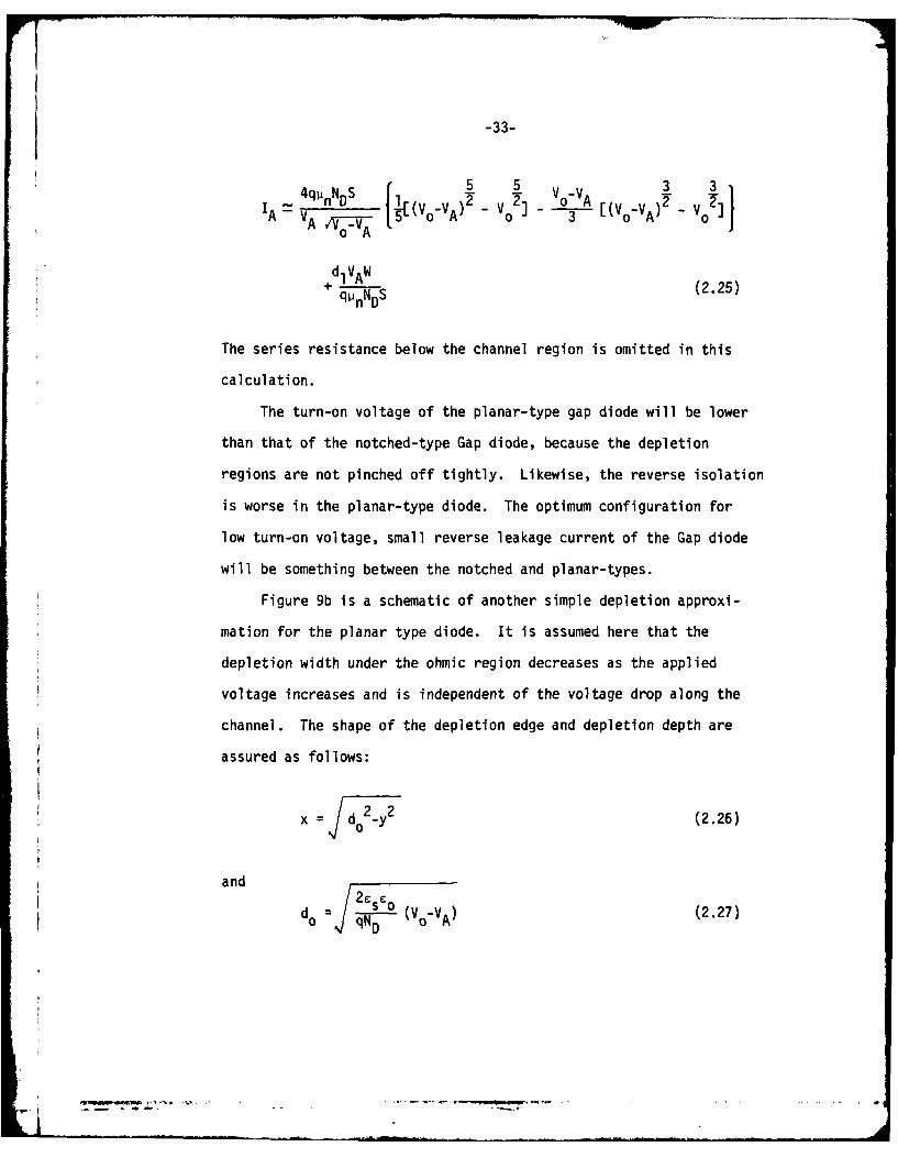
4qpnNDS 5 5 V3 3
VA _ OVoVA) V.7] -3 Vo]
1oA+dV-D (2.25)
The series resistance below the channel region is omitted in this
calculation.
The turn-on voltage of the planar-type gap diode will be lower
than that of the notched-type Gap diode, because the depletion
regions are not pinched off tightly. Likewise, the reverse isolation
is worse in the planar-type diode. The optimum configuration for
low turn-on voltage, small reverse leakage current of the Gap diode
will be something between the notched and planar-types.
Figure 9b is a schematic of another simple depletion approxi-
mation for the planar type diode. It is assumed here that the
depletion width under the ohmic region decreases as the applied
voltage increases and is independent of the voltage drop along the
channel. The shape of the depletion edge and depletion depth are
assured as follows:
x do2-y2 (2.26)
and
d= Q VoVA) (2.27)=[VDVs
, ,, , .. . ...

-34-
The diode current may be written as
IA VA (2.28)dy + -d
0 q Nd- y WSFxquN DnND S(W-2jdo2y2)nD
where V is the thickness of the epitaxial layer. The series resis-
tance under the channel region is taken into consideration and F is
a number larger than one which is used as a factor to obtain the
approximate cross-section area for the series resistance.
The integration in Equation (2.28) can be evaluated analyti-
cally and the current expression can be written as
1A VAIA I 7=2A tan-1 K+11 V-d0 (2.29)
2qpnNDS [-- + Tan- +K_1 q N "d°1 - K IK71
where
KW= Wd0
Equation (2.29) is an crude current-voltage approximation which may
be used to estimate the diode turn-on voltage and I-V characteris-
tics of the diode. The forward current will increase faster than
that of the preceding method.
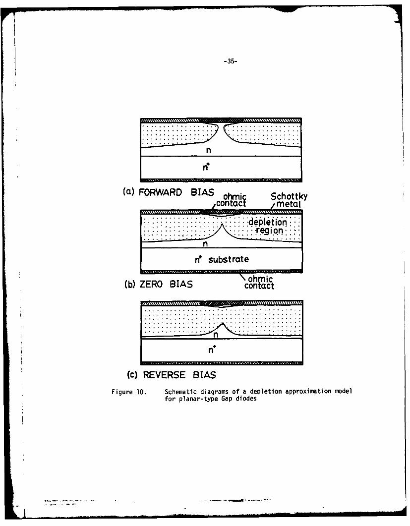
Figure 10 shows schematic diagrams of the depletion approximation
model for a planar-type Gap diode under (a) forward bias (b) zero
bias and (c) reverse bias conditions. In the diagram the depletion
. ... .... .... .. .. . .. .. l .. ... l l.. .... -1
-35-
........... nn
(a) FORWARD BIAS Schottky... ,,,.... ,,,,,,' /contac .. ,,,,metal
:ePletion:". . . .. ..
n
nf substrate
(b) ZERO BIAS contact
. . . . .o • ,. . . . , • • . . .... • , . , ,
(c) REVERSE BIAS
Figure 10. Schematic diagrams of a depletion approximation modelfor planar-type Gap diodes

-36-
region is pinched-off slightly under zero bias. Therefore, the
reverse current isolation is improved at the expense of high turn-on
voltage. A good diode is a unidirectional device with efficient
rectification, hence high reverse leakage will degrade the performance
of the diode drastically. Fabrication technology and experimental
results of the planar-type Gap diode are presented in the following
chapters.
.* . 1

-37-
3. VAPOR PHASE EPITAXIAL GROWTH OF GaAs
In this chapter we describe the epitaxial reactor and techniques
employed for the growth of GaAs layers used in Gap diode fabrication.
3.1 DESCRIPTION OF EPITAXIAL REACTOR
GaAs epitaxial layers are grown in an AsCt 3-Ga-H 2 flow system of
the type first described by Knight et al. [28]. A schematic diagram
of the reactor and two-zone furnace is shown in Figure 11. This
appears to be intrinsically a simple and reliable system and has the
advantage over other systems that all the starting reagents are ob-
tainable in a state of high purity. Efforts have been directed,
first, to reducing impurities in the system, and second, to con-
trolling physical growth processes which cause variations in elec-
trical properties.
The two-zone furnace has two independent temperature controllers.
The temperature profile of the furnace is shown in Figure 12. The
reactor tube, seed holder and melt boat are constructed of quartz.
All the gas lines up to the flow valves, except the aluminum H2S
dopant line, are stainless steel. The AsCZ3 bubbler is constructed of
Pyrex and cooled by a constant temperature refrigerated circulator
attached to the water bath.
The furnace is mounted on a wheeled stage so that it can be moved
along the reaction tube to heat or cool the reactor quickly, thereby
shortening the exposure time of the arsenic-saturated Ga source under
the hot hydrogen flow before and after the growth time. Dissolution
of GaAs crusted over the Ga source was observed when it was exposed

-38-
H2
BypH 2S*H2
Cstaet~Temperatur Gas~ Sorc
Figueb1. oShmai of Bubble-2 apr phae eitaia
Exsystet
-t d;

-39-
900,
101
I-r~800W
H700
LL GoSucGaAs Substrates Ga Source
0 6 12 18 24DISTANCE (In)
Figure 12. Temperature profile of the furnace. Curve (a) isused for the Ga-baking in H2 and saturation with Asof Ga source. Curve (b) is for the epitaxialgrowth

-40-
for a time to hot hydrogen bypassing the AsCZ3 bubbler. This dis-
solution correlates with an interfacial dip of the concentration
profile.
After construction, the system was dismantled, the quartz and
Pyrex parts cleaned thoroughly in aqua regia and rinsed in deionized
water, the stainless steel tubing cleaned using isopropyl and tricho-
loroethylene (one part each), and dried by nitrogen. The system has
been checked for leak-tightness at each joint.
To prepare the reactor for growth the AsC£3 (Mining and Chemical
Products, 99.999% pure, in 1Og ampoules) is loaded and hydrogen
passed through it for several hours to distill off the first fraction.
If this is not done, the first epitaxial layer will have a higher
carrier concentration than normal. The final clean-up of the system
to remove impurities is carried out by raising the furnace temperature
to 930'C and flowing H2 through the AsCZ3 to etch the reactor tube.
3.2 SOURCE SATURATION
The epitaxial growth of GaAs in this open tube system may be
separated into two distinct processes: 1) source saturation and
* transport, and 2) epitaxial growth on the substrate surface. Prior
to transport and epitaxial growth the Ga source must first be satu-
rated with arsenic until a crust of GaAs forms over the liquid gallium
surface. After the saturation process is complete, transport occurs
from the source to the deposition region with subsequent epitaxial
growth.
The gallium (99.99999% pure, 25 g ingots) is loaded in the
source boat of the reactor. Figure 12 shows the temperature profile

-41-
of the two-zone furnace. The source temperature is about 8800C. High
purity hydrogen from a palladium diffuser bypasses the AsCZ 3 bubbler,
whose flow rate is set to 120 mt/min. The hydrogen flow rate in the
dopant line is set to 200 me/min. After one hour Ga source baking,
the valve of the bubbler is opened and hydrogen is bubbled through the
AsCtZ3 liquid (kept at 15°C).
During the saturation process, the hydrogen, as a carrier,
transports the AsCZ 3 into the reactor. The initial reaction taking
place when the gas mixture heats up is
4AsCZ3 (g) + 6H2 (g)- -12HCZ (g) + As4(g) (3.1)
After adding the AsCZ 3 into the reactor, arsenic is continuously
dissolving in the gallium source
Ga(t) + As4(g) - Ga(As) solution (3.2)
while the gallium is simultaneously removed by reaction with HCZ to
form volatile gallium chlorides according to the following equations:
2Ga(t) + 2HCt(g) - 2Ga(g) + H2(g) (3.3)
2Ga(Z) + 6HCZ(g) -- 2GaCl 3(g) + 3H2(g) (3.4)
During saturation the source remains a bright homogeneous liquid. As
the solution becomes saturated, a GaAs crust starts to form over the
- ---

-42-
low temperature region of the source, since the GaAs is less dense
than Ga. As more arsenic is dissolved the crust extends to higher
temperature regions. Finally, sufficient arsenic is dissolved to
extend the crust completely over the entire source. That the source
is saturated to produce a complete crust can be determined by visual
observation. A completely crusted source is unstable in the absence
of an AsCt 3 flow. This is due to crystallization and thickening of
the crust in the low temperature region with subsequent dissolution of
the crust at the higher temperature regions. Therefore, source
stability is promoted by a minimum temperature gradient over the
source boat.
After about 8 hours of saturation under the preceding conditions,
the gallium source is visually checked for saturation, the AsCZ3 and
the furnace are turned off and hydrogen flow rate lowered to
60 nt/min. The system is now ready for epitaxial growth.
3.3 EPITAXIAL GROWTH PROCEDURE [29]
In the source region, the saturated source, polycrystalline
gallium arsenide, is attacked by HCt around 8400C and the following
reaction takes place:
8400C
4GaAs + 4HCt = 4GaCt + As4 + 2H2 (3.5)
7500C
At a lower temperature, in the substrate region (e.g. 7500C), solid
GaAs is deposited partly by the inverse reaction, Equation (3.5),
and partly by the reaction:

-43-
7500C
6GaCZ + As4-- 4GaAs + 2GaCt 3 (3.6)
Since hydrogen is used as a carrier gas, the reaction of Equation
(3.5) must be dominant. When the carrier gas is an inert gas (e.g.
argon), the dominant equilibrium will be reaction given by Equation
(3.6).
Because of differences in reactor design, residual impurities and
other factors, the optimum growth conditions vary from one reactor to
another. Typical growth conditions are: Ga temperature from 8200 to
8600C, growth temperature from 7200 to 760'C, growth temperature
gradients from 50 to 150C/cm.
The growth procedure is as follows: the furnace is turned on to
the desired temperature settings first, while the reactor tubing is
not in the furnace. The prepared GaAs substrate is loaded in the
growth region. After the reactor tubing is properly flushed with high
flow rates of hydrogen, then the hydrogen flow rates in the carrier
line (with the AsCZ3 bypassed) and the dopant line are adjusted for
220 ml/min and 200 m/min, respectively. Then the hot furnace is
moved into the growth position. After about 10 minutes, the furnace
temperature again approaches its steady state value, the hydrogen flow
is turned through the AsCZ3 bubbler for initiation of growth. After
the AsCU3 has been turned on for 5 minutes, then the hydrogen flows in
both the carrier and dopant lines are reduced to 120 mZ/min and
50 m/min, respectively.
__________ - -. .... . .
-44-
The carrier concentration of epitaxial layer can be increased
properly by adding H2S dopants in the dopant line. After the desired
growth time, the hydrogen is switched to bypass the AsCt 3 bubbler and
the remainder of AsCt 3 in the reactor is purged for two minutes. Then
the furnace is moved away to cool the reactor quickly. Generally, the
growth rate decreases as the temperature gradient decreases. Pyramid
formation during epitaxial growth is more pronounced at low growth
temperature and at high ASCL3 temperature and also due to the increase
in the amount of Ga. On the other hand, a decrease in the density of
pyramids is observed when the flow rate of H2 is lowered. The density
of these undesirable pyramids is dramatically reduced using substrates
with small misorientations (20 to 50) from (100) direction.
3.4 H2S DOPANT INCORPORATION
The incorporation of sulfur in GaAs can be written in two steps
consisting of the dissociation of H2S and dissolution of sulfur [30].
The dissociation reaction is
H2S(g)---H 2 (g) + S2(g) (3.7)
The dissolution process may be written as
II
.S 2(g)-'S (in GaAs) (3.8)
The overall process of doping with H2S is the sum of reaction of
Equations (3.7) and (3.8)

-45-
H2S(g)--H 2(g) + S (in GaAs) (3.9)
One of the relations between the flow rate of H2S dopants (10 PPM in
N2) and the carrier concentration of the grown layer measured by the
capacitance-voltage method is shown in Figure 13.
Sulphur does not form stable chlorides and the free sulphur
equilibrium is only affected by the hydrogen and the H2S concentra-
tion. Therefore the sulphur-doped carrier concentration is not
affected by the AsCt3 mole fraction, compared to germanium or
selenium-doped crystals [31].
3.5 SUBSTRATE PREPARATION [32]
The epitaxial layers were grown on silicon doped substrates with
carrier concentration 2 x 1018 cm"3 . The crystallographic orientation
is 20 off the (100) plane to prevent the formation of pyramids.
After the substrates are cleaved to desired dimensions, they are
cleaned with organic solvants, trichloroethylene, acetone and methanol
in sequence, in a beaker. The substrate is dried with bibulous paper
and nitrogen. The sample is then stir-etched in a 5H 2S04 : 1H202
1H20 solution for two minutes. This etchant has been mixed and cooled
for ten minutes. The substrates are then rinsed in deionized water,
and dried with bibulous paper and nitrogen, and loaded immediately in
the reactor. The reactor is then flushed with hydrogen at high flow
rates for 20 minutes before the furnace is moved to the growth position.
3.6 MATERIAL EVALUATION
The grown layer thickness is measured by the stain etching
method. The sample is cleaved, etched in a mixture of
-.. .... . ... . . . ...- .. - * .,r Naml - - nf ,w-.

-46-
0
S1017-
w
01
IT, 10 101102
FLOW RATE OF H2S (10 ppm In N2 ) IN mi/MIN
Figure 13. Doping density as a function of H2S flow rate

-47-
lHF : 3HNO3 : 4H20 for about seven seconds, then viewed edgewise in a
calibrated microscope. The measurement resolution is limited by how
well the microscope could focus on the top rounded surface of epitaxy
and interface. Depletion capacitance-voltage measurement may give a
more accurate determination of epitaxial layer thickness.
The carrier concentration profiles of epitaxial layers are
measured by differential capacitance technique, using 20 mil diameter
dot aluminum Schottky barrier diodes. The aluminum dot is negatively
biased with respect to the substrate and the capacitance of the deple-
tion region is measured as a function of the applied bias. The doping
concentration is calculated from the measured C-V data.
The effective depletion width is calculated from the measured
capacitance by the simple relation
d =- A (3.10)C
where d = depletion depth into the epitaxy
A = dot area
C = depletion capacitance
The range of d over which the carrier concentration can be
measured is limited by avalanche breakdown of the reverse-biased
Schottky-barrier. The profiling of a layer with concentration varia-
tion can be obtained by step etching the layer to build up a piecewise
profile plot.

-48-
One of the problems which often occurs in GaAs epitaxial growth
is the existence of a dip in carrier concentration profile between the+
n layer and the n substrate [33,34]. Growing a moderately doped
buffer layer onto the substrate prior to the growth of the n layer can
reduce the possibility of having a interfacial dip of the concentra-
tion profile.

-49-
4. DEVICE FABRICATION
In this chapter the fabrication process for Gap diode is described.
4.1 DEVICE CONSTRUCTION
The geometry of the device is a quasi-planar structure as shown
in Figure 14. The n-type epitaxial layer is grown on Si doped, (100)
+oriented, n GaAs substrate as described in Chapter 3. The thickness
of the epitaxial layer is 1 Pm and it has a carrier concentration of
2 x 1015 cm-3 . Sulfur (H2S) is used to dope the buffer layer. The
carrier concentration profile of a representative layer is shown in
Figure 15. The wafer thickness of the completed device is 80 um. The
diameter of the diode is about 30 um; it can be slightly reduced by
GaAs mesa etching. The widths of the ohmic contact gaps can be
varied from 2.6 pm to zero. A vacuum evaporated SiO layer is used to
isolate the substrate from the bonded 1 mil gold wire when the devices
are packaged.
4.2 OHMIC CONTACT FABRICATION
The GaAs wafer is first mounted on a jig by using black wax with
the epitaxial layer side down. The back of the sample is slowly
lapped with 5 pm grit on a glass plate. The thickness of the sample
is measured with a micrometer. The sample is then mounted on a glass
slide using black wax to mask the epitaxial layer and then etched in a
5H2S04 : 1H202 : 1H20 solution. The etchant is first stirred and
cooled for 10 minutes. The substrate is put in the etchant and
stirred for about 10 minutes to obtain a smooth surface. The measured
resultant substrate thickness is 80 um. The sample is then rinsed in
deionized water and dried.

-50-
Au
GaAs NSUBSTRATE
SOHMIC '
Figure 14. Cross-section of planar-type gap-controlled GaAsScottky-barrier diode

-51-
Es j~I9Surf ace
z0
108nSubstrate
z
z0
01
< 105 k."Active Region
02 3DEPTH I N SUBSTRATE (urn)
Figure 15. Carrier concentration versus depth for VPE grownlayer from Schottky barrier profile measurements

-52-
After etching, the sample is loaded in a vacuum evaporator. AuGe
is evaporated on the substrate side followed by a nickel evaporation.
The AuGe used is eutectic composition of 88% Au, 12% Ge by weight.
The thicknesses of the evaporated AuGe and Ni are monitored, the
thickness ratio is about 4:1 to obtain thermally stable contacts with
low contact resistance. The AuGe-Ni layer is alloyed in a furnace at
456°C for 35 seconds in a hydrogen atmosphere. The wafer is quenched
by removing it quickly.
4.3 SCHOTTKY-BARRIER FABRICATION
The sample is mounted, ohmic contact side down, on a glass slide
with black wax. It is then cleaned in organic solvents, trichloro-
ethylene, acetone, and methanol, and the epitaxial layer is slightly
etched in a prepared 5H2S04 : lH202 : 1H20 etchant. After the sample
is rinsed in deioni ed water and dried, it is prebaked at 1200C for
3 minutes. Then a positive photoresist, AZ1350J is spun on the sample
at 10,000 RPM for 50 seconds. The photoresist is baked for 25 minutes
at 750C.
An optical mask aliqner is then used to expose the photoresist.
The mask contains 2.2 um dark fringes with 1.8 pm spacings. The
fringes are aligned along a cleavage plane. The exposed photoresist
is developed and is then dried and postbaked for 6 minutes at 1200C.
The width of the photoresist lines slightly depends on the exposure
time. A photograph of the photoresist lines is shown in Figure 16.
At this stage the sample appears in cross-section as in Figure 17(a).
The sample is loaded in an evaporator, and 900A thick AZ is evapo-
rated on it as shown in Figure 17(b).
7 ..

Ii
-53-
S
i
Figure 16. Photograph of 1.5 um photoresist grating patternon the GaAs epitaxial layer

-54-
(a)
Photaruist-- AuG*.Ni1 Al or Ni
C) n IwLayerI______________ + Subut'mt
Ohmc Contc
Figure 17. Process used to fabricate planar-type gap diodes
-55-
4.4 JUNCTION FORMATION
The photoresist mask is lifted by using photoresist stripper
(Shipley Remover 140). After the sample is rinsed in deionized water
and dried, it is loaded in the evaporator again. This time 800A AuGe
and 200 A Ni are evaporated, respectively, on the AZ lines and gaps of
the sample. Then the wafer is alloyed at 4560C for 35 seconds in a
hydrogen atmosphere. The preceding fabrication process is shown
schematically in Figure 17(c).
The wafer is then rinsed in hydrofloric acid for 10 seconds and
rinsed in deionized water. A gold layer of about 2 um is applied to
the ohmic contact by plating the wafer in a neutral bath gold solution
(Selrex Puragold 125) at 65°C. The result is shown in Figure 17(d).
After gold plating the wafer is mounted on a glass side with
substrate side down. It is cleaned in organic solvents, trichloro-
ethylene, acetone, and methanol and prebaked again at 1400C for 15
minutes. Then filtered AZ1350J photoresist is spun on the sample at
3500 RPM for 40 seconds, and baked at 750C for 30 minutes. The
photoresist is exposed in a pattern of 32 pm diameter dot matrices.
The pattern is aligned along a cleavage plane. The exposed photo-
resist is developed, dried and postbaked at 200*C for 40 minutes. The
resultant top-view picture is shown in Figure 18.
The hardened photoresist dot is used as a mask to etch the thick
Au, AuGe-Ni alloy and AZ lines. The etchant is Aurostrip powder
diluted in deionized water. The Aurostrip solution is heated and
stirred, the wafer is immersed until all the AZ and AuGe/Ni lines in
between the dots are etched. The junction will be undercut more or
-!* 1= -....

-56-
Vi :
II Fiur ... Po grps of 32 Pm dimtr.o o r t dot on
the~ almiu "aod •u N lines

-57-
less through the photoresist mask. One of the methods to reduce this
undercutting is to make the ohmic contact and Aluminum lines thinner.
Figure 19 shows unalloyed A1/AuGe/Ni dots on GaAs after metal etching.
4.5 GaAs MESA ETCH AND SiO INSULATION
After junction formation etching, the wafer with photoresist dots
on it is rinsed in deionized water and baked in 120°C for 10 minutes.
Then the wafer is etched in a prepared 5H2SO4 : 1H202 : 1H20 solution
to form a suitable GaAs mesa structure. At this juncture the diode
area can be reduced by mesa etching the GaAs.
The wafer is rinsed in deionized water and again baked at 1200C
for 10 minutes. Then it is loaded in the vacuum evaporator, and 7000 A
to 9000 A SiO (99% pure, powder) is evaporated on the wafer, as shown
in Figure 17(e). The photoresist dots are lifted by using photoresist
stripper, and the fabrication is completed. Figure 20 shows photo-
graph of several completed Gap diodes on a GaAs chip.
4.6 PACKAGING
To obtain packaged devices, the completed wafer is scribed into
chips with approximately 3 x 3 diodes per chip. The chip is ultra-
sonically bonded in a C-2 package [35], the dimensions of the package
are shown in Figure 21. Two 1 mil diameter gold wires are bonded
across one diode on the chip. The photograph of the unsealed packaged
diode is shown in Figure 22. Finally, the diode package is sealed
with a metal lid on top of it.
In the next chapter evaluation methods and experimental results
for the packaged diodes are presented.
-~ ~--v.-~r.. .........

-58-
~Nk
(
O~ 0"
II
Figure 19. Photograph of unalloyed AZ/AuGe/Ni stripe dots onGaAs surface after metal etching

-59-
Figure 20. Completed Gap diodes on a scribed GaAs chip
-60-
CASE STYLEC-2
LP<l1nHCp<.1 pF
-- o,.030-
T
.158__ _ _ _ _
I.020x.030 SLOT
Figure 21. Dimensions of the diode package [35]

K -MIR
-61-
Figure 22. Photograph of a GaAs Gap diode chip mounted on aC-2 package, bonded with 1 mili Au wires

-62-
5. EXPERIMENTAL RESULTS AND DISCUSSION
In this chapter we examine the experimental behavior of the Gap
diode. We will evaluate the diode current-voltage characteristics.
the temperature dependence of the I-V characteristics and some of
the microwave behavior of packaged devices.
5.1 CURRENT-VOLTAGE CHARACTERISTICS
Diodes were made from various thicknesses and doping concentra-
tions of epitaxial GaAs. However, the electrical characteristics
of only those diodes processed from low doped, n=2xlO 15 cm-3, epi-
taxial layers will be discussed. The dimensions of the ohmic gap
width are limited by the photolithography to 1 pm to 2 um. The zero
bias depletion width from the depletion approximation, for n=2xlO15
cm-3, and built-in voltage Vo=O.7 V, is about 0.7 um.
Figure 23 shows various measured low-frequency I-V characteris-
tics of the planar-type Gap diode, as the ohmic gap width, W, is
gradually increased from zero to more than two depletion widths.
Notice that turn-on voltages ranging from 0.7 V to nearly zero can
be obtained. The diameter of these diodes is 30 um. The right-most
I-V curve in each figure is for an AZ Schottky diode made by the
same fabrication procedure as the Gap diodes. The reverse isolation
of the planar-type Gap diode is not as good as that of the notched-
type Gap diode. Hence, as the ohmic gap width opens, the reverse
leakage current becomes large, as can be seen in Figure 23.
The I-V characteristics of two typical low leakage packaged
planar-type Gap diodes are shown in Figure 24 on expanded scales.
I.

-63-
=iE
i
Figure 23. Photographs of various measured low-frequency I-Vcharacteristics of the planar-type diodes as ohmicgap width, W, is gradually increased from zero tomore than two depletion widths

-64-
i
Figure 24. Photographs of I-V characteristics measured fromtwo typical low-leakage packaged planar-typeGap diodes (Gap diode U-2, U-5)
-65-
These devices have I-V characteristics similar to those of point
contact diodes, although the Gap diodes are made with very low
doped epitaxial layers and large diode areas in contrast to point
contact diodes.
Figure 25 shows the I-V characteristics of two wider gap-
width packaged planar-type Gap diodes which show significant
reverse currents. Although the turn-on voltages are low, because
of the large reverse currents and corresponding low ratios of
reverse resistance to forward resistance, these diodes will not
yield desirable RF performance. Figure 26 and 27 show the
representative I-V characteristics of two different low leakage
Gap diodes on two different scales for each diode, respectively.
The diode in Figure 27 has a wider ohmic gap width than that
in Figure 26. These figures show that the turn-on voltage is
reduced at the expense of reverse leakage current.
A detailed comparison between a Gap-diode and a pure At Schottky
diode of the same size is shown in Figure 28. The turn-on voltage
of the Gap diode is lowered by 0.3 volt compared to that of the
pure Schottky diode, with the reverse leakage current increased not
more than one order of magnitude. The I-V relationship of the Gap
diode in the forward direction still follows an exponential
behavior in the low current region.
The ideality factor of the diodes calculated from the slopes
in Figure 28 is about n=1.5. Conventional Schottky barrier devices
typically have n=l.02. One possible explanation for this large
value is that the diodes are made from low doped epitaxial layers

-66-
I'I-
II
Figure 25. Photographs of I-V characteristics measured from twowide gap width packaged planar-type Gap diodes(Gap diodes T-9, E-8-8)
. . . . . .I

-67-
Figure 26. Photographs of I-V characteristics of a packagedplanar-type Gap diode with two different currentand voltage scales (Gap diode U-4)
-68-
Figure 27. Photographs of I-V characteristics of a packagedplanar-type Gap diode with two differenc currentand voltage scales (Gap diode T-3)

-69-
(M.
0~0>
@0 I-
4-F_.
0
o0 '0 10 b 0 0(edwV) .LN388n:)
Figure 28. Representative I-V characteristics ofa low-leakage Gap diode and a pure AtSchottky diode of the same size

-70-
and, therefore, the diode series resistance becomes large. Another
reason may be that the Schottky-barrier junction has been alloyed
at high temperature (456C) in the fabrication procedure. High
temperature anneals can degrade the properties of Schottky-barrier
junctions [36].
Figure 29 compared the measured forward I-V characteristics
of several Gap diodes and a pure At Schottky diode. The dif-
ferences in these I-V curves may be due to the effect of diode
mesa area variations, difference in ohmic contact and Schottky
contact widths, and diode packaging variations.
The Gap diode T-9, shown in Figure 29, possibly results from
bonding two adjacant diodes on the chip. This would account for
both the large initial slope and larger current at high voltage.
At high current levels, the I-V relationship tends toward a
resistance fixed by the conducting channel resistance.
Notice that in Figures 28 and 29, the currents of all the Gap
diodes and the Schottky diode tend to the same value for large applied
voltage. For the Gap diode, when the depleted regions are fully
retracted, current is-carried by the ohmic gaps and the Schottky
barriers, i.e. the entire diode area is supplying current. Likewise,
the entire area of the Schottky diode always supplies current. At
high voltages, the effective areas of both types of devices are
equal.
5.2 DIODE CAPACITANCE
The capacitance of the Gap diode is a depletion capacitance.
It can be thought of in terms of two components; depletion under

-71-
0.1 I I I I -_
=D> > >-
-o
O
0
0
diode
- '-'vd
-72-
the Schottky metal and that due to depletion in the gap under the ohmic
metal. Preliminary capacitance measurements from packaged diodes show
that, in the reverse bias direction, the capacitance decreases slightly
then remains almost constant; in the forward direction, the capacitance
increases rapidly beyond a bias larger than a few tenths of a volt.
This is to be expected for the thin, low doped layers used. The deple-
tion region under the Schottky contacts is punched through to the
conducting substrate.
The charge distribution near the ohmic contact is complicated and a
precise understanding of it is not yet well in hand. However, if one
considers the model suggested in Figure 10, it can be seen that the
depletion width under the ohmic contact is less than that under the
Schottky metal, leading to an increased capacitance in the gap. Thus,
one would expect that the zero bias capacitance of the Gap diode should
increase with increased gap width until the gap is made so large that
the adjacent depletion regions separate.
5.3 TEMPERATURE DEPENDENCE OF THE I-V CHARACTERISTICS
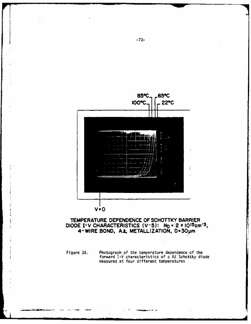
The temperature dependence of the forward I-V characteristics of a
At Schottky diode measured at four different temperatures is shown in
Figure 30. The turn-on voltage of the Schottky diode is reduced by
about 80 mV when the temperature is increased from 22C to 1000C. The
Schottky-barrier height is decreased as the temperature is increased,
because thermionic-emission dominates in the forward bias region.
However, the ideality factor decreases as temperature increases. At
very low temperatures (T < 2000 K), the forward I-V characteristics tend
to become independent of temperature (37). This suggests that at low
........."-,.--- li ~ limI mm i i mm
-73-
V650
850C- 220C
V-O
TEMPERATURE DEPENDENCE OF SCHOTTKY BARRIERDIODE I-V CHARACTERISTICS (V-5): ND x 2 x 1015 cm-3 ,
4-WIRE BOND, AA, METALLIZATION, D-3Ojjm
Figure 30. Photograph of the temperature dependence of theforward I-V characteristics of a At Schottky diodemeasured at four different temperatures
-74-
temperatures there is a strong tendency towards quantum-mechanical
tunneling.
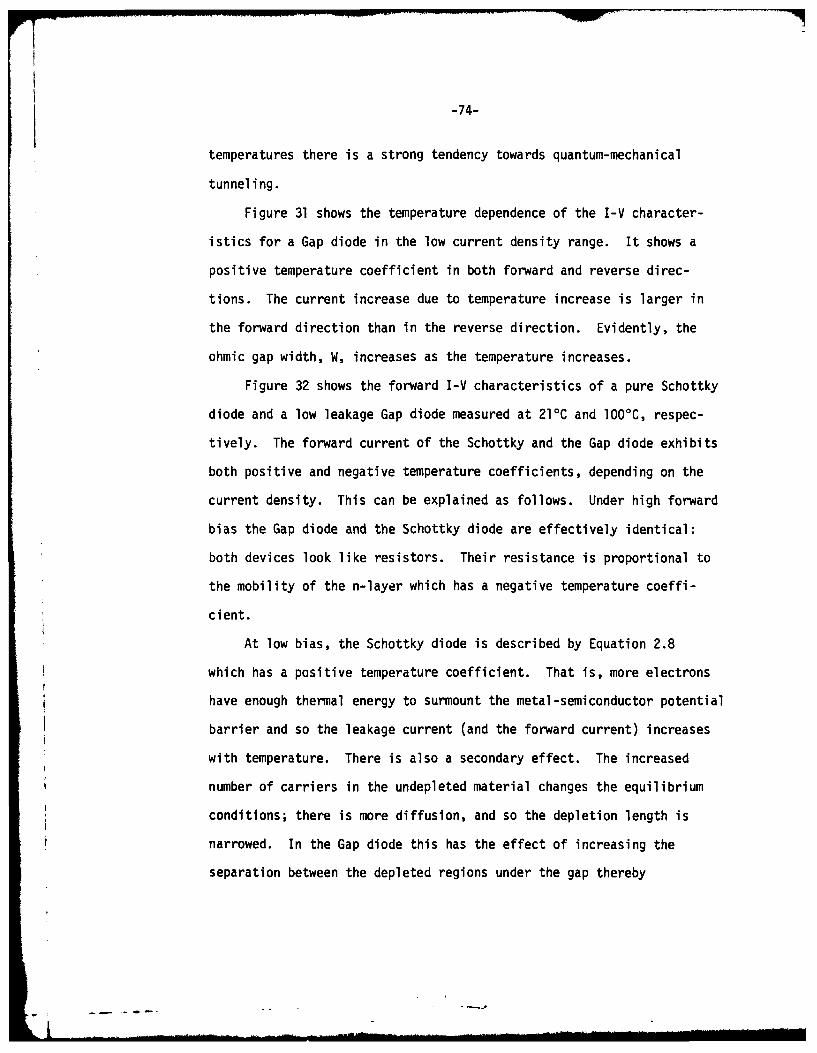
Figure 31 shows the temperature dependence of the I-V character-
istics for a Gap diode in the low current density range. It shows a
positive temperature coefficient in both forward and reverse direc-
tions. The current increase due to temperature increase is larger in
the forward direction than in the reverse direction. Evidently, the
ohmic gap width, W, increases as the temperature increases.
Figure 32 shows the forward I-V characteristics of a pure Schottky
diode and a low leakage Gap diode measured at 210C and 1000C, respec-
tively. The forward current of the Schottky and the Gap diode exhibits
both positive and negative temperature coefficients, depending on the
current density. This can be explained as follows. Under high forward
bias the Gap diode and the Schottky diode are effectively identical:
both devices look like resistors. Their resistance is proportional to
the mobility of the n-layer which has a negative temperature coeffi-
cient.
At low bias, the Schottky diode is described by Equation 2.8
which has a positive temperature coefficient. That is, more electrons
have enough thermal energy to surmount the metal-semiconductor potential
barrier and so the leakage current (and the forward current) increases
with temperature. There is also a secondary effect. The increased
number of carriers in the undepleted material changes the equilibrium
conditions; there is more diffusion, and so the depletion length is
narrowed. In the Gap diode this has the effect of increasing the
separation between the depleted regions under the gap thereby
-75-
85°CIO0=C _ 64°C
1206C_145°C0 220C
V=O
TEMPERATURE DEPENDENCE OF GAPDIODE (V2): No a2 xIOIScm 3 ; 4-WIRE BOND, D a3Opjm
Figure 31. Photograph of the temperature dependence of I-Vcharacteristics for a Gap diode
Lt

-76-
gow
a)0
A 0o 0 0 0 0
(SdW) iN~If%Figre 2. orardI-Vchraceritis o a4ur
Scotkydod (P)an Gp id(U-) masued t 2 0C nd OO6
respectivel
-77-
increasing the current. Presumably, the current in the Gap diode
rises more slowly with temperature then in the Schottky case because
the reduction in depletion width is a second order process, while
the increase in current in the Schottky is proportional for T2 and
the exponential factors of Equation 2.8. This difference can be seen
in Figure 32 by examining the change in current with temperature at
constant (low) voltage compared to the effect of the thermally
generated carriers coefficient.
A comparison of the temperature dependence of the I-V characteris-
tics of a Si point contact diode (IN23C) and a low leakage GaAs Gap
diode is shown in Figure 33a and b. The measurements are made at three
different temperatures, 220C, 80C and 920C, respectively. The I-V
characteristics of the Gap diode show less temperature sensitivity than
those of the point contact diode. Notice that in the reverse bias
direction, the point contact diode has larger leakage current.
5.4 DETECTOR CHARACTERISTICS
Figure 34 compares the open-circuit detected output voltage versus
incident RF power of a low leakage Gap diode to those of a Si point
contact diode (lN23C) and a At Schottky diode at a frequency of
10.565 GHz. The Schottky diode is made with the same fabrication pro-
cedure as the Gap diode. All the measurements are done using the same
X-band waveguide diode mount. No DC bias is applied.
The Gap diode exhibits about 3/4 the sensitivity of the IN23C but
saturates at higher power levels. When compared to a conventional
Schottky diode the advantage of low turn-on voltage is readily apparent.
-~, '~,.l

-78-
A.
V;.
I-V CURVES WITH TEMPERATURE AS PARAMETERA. 1N23C: POINT, CONTACT DIODE
809C
r-V CURVES WITH TEMPERATURE AS PARAMETERB. GAP DIODE (V-2): N0) a2 aIO 15cn 3 4-WIRE BOND,
Figure 33. Photograph of temperature dependence* of I-V characteristics of (a) a point
contact diode '(1N23C) (b) a Gap diodeat 220C, 800C and 920C

-79-
I -_
-j-
0
=ti
0
CP
zz l --"--ziw
- IN23C Pure Schottky
Diode UP-4S 2 Gap Diode
v-10
0
-o
0 1-
-50 -40 -30 -20 -10 0 10 20INCIDENT POWER IN dBm
Figure 34. Open-circuit voltage output versus incident RFpower for Gap diode (V-10), point contact diode(1N23) and Schottky diode (UP-4) at 10.565 Ghz
. . . . . . . .. . ~ c .I h n n q m * in , ad-m D a o. - ' ..

K7.
-80-
The characteristics of this device makes it a good candidate for
control applications where good sensitivity and wide dynamic range are
desirable.
Devices which exhibit high detectivity also have low reverse
leakage current. Hence for good high frequency performance large
reverse isolation, low junction capacitance and low series resistance
are required. Notice that the diameter of the Gap diode used in these
experiments is 30 um, which is very large compared to that of the
point contact diode, typically 2 um. For a device design when the
diode is punched-through in zero bias, the product of capacitance
times voltage depends on (ND)Ir1 . Thus with increased carrier con-
centration improved performance at higher frequencies is expected.
Zero-bias detection sensitivity measurements have been carried
out at several frequencies ranging from 10 to 70 GHz using the same
diode in a coaxial mount, iris coupled to an input waveguide. Al-
though these large diameter, low doped devices are far from optimum
for operation at such high frequencies, surprisingly good results were
obtained as seen in Figure 35.
5.5 MIXER CHARACTERISTICS
A single-ended mixer setup, as shown in Figure 36, was used to
measure the conversion loss of the Gap diode. The IF impedance
transformer was chosen to provide a 509 to 400a transformation. The
adjustable matching network is an LC r circuit. The best device
showed conversion loss of 6.1 dB at 10.5 GHz, including 1 dB insertion
loss in the 20 MHz IF impedance matching network. The lowest conversion
loss observed for the 1N23C point contact diode in the same mount is 9 dB.
(W

-81-
I--0
0
0
002
S -_
Q -
W A
9Lo I0-
I0
-5 -4 -3 2 1 02
INCDENGAP DIODE V-Opowr oo 10.5GHz
10-3 • 30-Z • 60am
0 7
-50 -40 -30 -20 -I0 0 I0 20INCIDENT POWER IN dBm
Figure 35. Open-circuit voltage output versus incident RF
power of a Gap diode (V-bO)
.. . . . Ii i.... .. l -- _ _ __ll .. . I

-82-
c"-))
IZDnUU
Figure 36. Single-ended mixer conversion loss measuring setup
HID Illl lllll~ l llllCI
-83-
Figure 37 shows conversion loss versus local oscillator power for
three Gap diodes with different ohmic gap widths at 20 MHz IF and
10.5 GHz RF. Gap diode U-3 has the smallest gap. Its conversion loss
is the lowest under high local oscillator drive conditions. As the
local oscillator power is decreased the conversion loss increases
rapidly, similar to the behavior of a conventional Schottky diode.
In Figure 37, the gap width of the diodes shown increases from
right to left. The conversion loss of diode U-7 in the high local
oscillator power region is larger than that of the other two diodes,
because of its larger reverse leakage. On the other hand, diode U-7
shows lower conversion loss at low local oscillator powers, owing to
its lower turn-on voltage. The measured conversion loss versus local
oscillator power relationship for the 1N23C point contact diode is
similar to that of Gap diode U-7. Consequently, the best Gap diode
for detector and mixer applications will be that with low turn-on
voltage and good reverse isolation.
The principal factors limiting diode performance are the junction
capacitance C. and series resistance Rs. Junction capacitance C.
allows current to bypass the nonlinear diode resistance R. while
series resistance Rs is a source of power dissipation, heat generation
and excess diode noise. The diode conversion loss is directly propor-
tional tothe product of diode junction capacitance and series resis-
tance. Therefore, better conversion efficiency and noise performance
are to be expected if the device carrier concentration is made higher
and the ohmic gap width and diode dimensions reduced.
. .. . . . . -.. ... ..- r ' l J l m ... . . -r ~ . .. ,

-84-
30"
% 25
020
015-
> 10-Z0~ *T-3
0 1 - - - -0 -20 -15 -10 -5 0 5 10
LOCAL OSCILLATOR POWER (dBm)
Figure 37. Single-ended mixer conversion loss versus localoscillator power for three different Gap diodes(at 10 GHz RF, 20 MHz IF). The ohmic gap widthincreases from diode U-3 to diode U-7
- -a-- I

-85-
6. CONCLUSIONS
A survey has been made of the techniques which may be used to
control and vary the effective barrier height of metal-semiconductor
diodes. The physical properties of Schottky-barrier and ohmic con-
tacts have been discussed. A new low turn-on voltage gap-controlled
Schottky diode and simple design theories for it have been presented.
Experimental results show the turn-on voltage of the Gap diode
can be controlled by varying the width of the ohmic gap. Some of
the I-V characteristics and detector sensitivites of the Gap diode
are similar to those of Si point contact diodes. Preliminary results
show the Gap diode to be less temperature sensitive than the point
contact diode. The burn-out properties of the Gap diode are expected
to be better than those of the pure Schottky diode, and its noise
properties also may be significantly different. The noise and the
burn-out behavior of the Gap diode need investigation.
Preliminary RF characteristic measurements show considerable
promise for the Gap diode. Its cutoff frequency can be increased
by reducing the ohmic gap width and the diode area, and by
increasing the epitaxial doping concentration. Optimum Gap diode
configurations for very high frequency applications need to be
explored, especially when high field transport in submicron
devices is considered. Better photolithographic technology is needed
for the fabrication of smaller ohmic gap widths. Other shapes of
gao openings, in addition to the two presented in this report, may
be considered.
2tU ~ I-

-86-
The depletion approximation picture of the Gap diode, as dis-
cussed in Chapter 2, is not sophisticated enough to accurately predict
all aspects of device performance. This is because detailed knowledge
of the free carrier distribution near the contact is not included in
the model. However, even such a crude representation is helpful in
understanding the influence of the geometric and material parameters
on device behavior. For example, the calculated results from the
analytic I-V relationship for notched-type diodes, shown in Figure 7,
have similar shapes to the experimental results obtained for planar-
type diodes. See Figure 29.
The I-V curves in Figure 7 are calculated using the condition
that the channel is not pinched off. That is, the zero bias depletion
regions in the gap do not touch. As the ohmic gap width W is increased,
the I-V relation deviates from the narrow gap exponential behavior to
a more linear (resistive) one. This prediction agrees well with that
observed experimentally as can be seen for the wide gap diode of
Figure 29, labeled V-9. Notice, also, that the currents for large
forward voltage (lOmA at V=IV) are well predicted by theory.
For the case of narrow gap devices, such as that represented by
diode U-2 of Figure 29, the analytical model fails since it predicts
zero current when the gap region is pinched off. In the physical
device, this is not the case since there will be a significant number
of free carriers within a few Debye lengths of the edge of the heavily
depleted region [38] which contribute to the current. Likewise, the
effect of the ohmic contact on carrier distribution in the gap is not
known in detail. It is likely that the ohmic contact is not truely

-87-
that, but rather a low barrier Schottky one. The influence of the low
barrier height will not be significant for wide gap devices where the
depleted regions separate with the application of a small forward
bias. However for narrow gap ones, since the potential drop laterally
(across the gap) will be small, the depletion regions will not retract
at the same rate as when the free channel is exposed, and so, the
influence of a low barrier contact may be magnified in this case. For
very small gaps the behavior is dominated by the Schottky contacts and
the I-V curve approaches that for a pure Schottky diode.
The electrical performance of a diode is a controlled by its I-V
characteristics. Since the Gap diode I-V relationship is not neces-
sarily exponential one might anticipate that non-linear effects such
as intermodulation distortion, harmonic generation, etc., may be
controlled by adjusting the shape of the I-V curve. For designing an
optimum diode configuration with low turn-on voltage, low reverse
leakage, and high cut-off frequency an efficient numerical analysis
will be required [39].
We have demonstrated a new device principle. It is possible to
produce depletion of carriers under ohmic contact regions. This
observation can be applied to other two and three terminal structures
which may yield microwave and millimeter wave devices with new and
desirable properties.
With the techniques discussed above, the effective barrier
height of metal-semiconductor contacts can be varied and controlled in
the range below the true barrier height. Therefore, it also may be
used as a tool or design approach for other device applications.
A..i-.... .. ... - - - - - -- -

-88-
7. ACKNOWLEDGEMENT
The authors wish to thank James E. Holtz and Bobby G. Atkinson of
the Central Microwave Company, St. Charles, Missouri, for helpful
discussions on device processing and assistance in device packaging.

AD-AI16 162 WASHINGTON UNIV SEATTLE DEPT OF ELECTRICAL ENGINEERING F/6 20/2CONTROL OF GAAS MICROWAVE SCHOTTKY DIODE ELECTRICAL CHARACTERIS-ETC(U)MAY 82 S J TENG. R E GOLDWASSER NOO014-79-C-040
UNCLASSIFIED TR-ONR-82-1 NL22IIIIIIIIND
1=I H2.2LIIIII '---" '° m
II11I1 I.l ---11111L25 111.8
MICROCOPY RESOLUTION TEST CHART
NATIONAL BUREAU OF STANDARDS 1963 A

-89-
8. BIBLIOGRAPHY
El) A.M. Cowley, H.O. Sorensen, "Quantitative Comparison of
Solid-State Microwave Detectors", IEEE Transactions
on Microwave Theory and Techniques, Vol. MTT-14,
No. 12, pp. 588-602, December 1966.
[2] Y. Anand, W.J. Moroney, "Microwave Mixer and Detector
Diodes", Proceedings of the IEEE, Vol. 59, No. 8,
pp. 1182-1190, August 1971.
[3) C.F. Genzabella, C.M. Howell, "Gallium Arsenide Schottky
Mixer Diodes", Institute of Physics Conference
Series Number 3, pp. 131-137 (1967).
[4) S.M. Sze, "Physics of Semiconductor Devices", Wiley,
New York (1969).
[5] E.H. Rhoderick, "The Physics of Schottky Barriers",
Oxford University Press, Oxford (1978).
[6) J. Bardeen, "Surface States and Rectification at Metal
Semi-Conductor Contact", Physics Review, 71,
pp. 717-727, (1947).
[7] C.A. Mead, "Ohmic Contacts to Semiconductors",Electrochemical Society (Edited by B. Schwartz),
pp. 3-16, (1969).
[8] R.A. Scranton, J.S. Best, J.O. McCaldin, "Highly
Electronegative Contacts to Compound Semi-
conductors", Journal of Vacuum Science and
Technology, 14(4), 930 (1977). I-!-,.

-go-
[9] J.M. Shannon, "Control of Schottky Barrier Height Using
Highly Doped Surface Layers", Solid-State Electronics,
Vol. 19, pp. 537-543, (1976).
[10] V.L. Rideout, "A Review of the Theory and Technology for
Ohmic Contacts to Group III-V Compound Semiconductors",
Solid-State Electronics, Vol. 18, pp. 541-550, (1975).
[11] W.J. Moroney, Y. Anand, "Low Barrier Height GaAs Microwave
Schottky Diode Using Gold-Germanium Alloy", 1970
Symposium on GaAs, Paper 31, pp. 259-267 (1970).
(12] C.J. Madams, D.V. Morgan, J.M. Howes, "Outmigratlon of
Gallium from Au-GaAs Interfaces", Electronic
Letters, Vol. 11(24), 574 (1975).
[13) G. Dearnaley, H. Freeman, S. Nelson, J. Stephen, Ion
Implantation. North Holland, Amsterdam (1974).
[14] J.M. Shannon, "Reducing the Effective Height of a
Schottky Barrier Using Low Energy Ion Implantation",
Applied Physics Letters, 24(8), 369 (1974).
[15) P.D. Taylor, D.V. Morgan, "The Effects of Radiation
Damage on the Properties of Ni-nGaAs Schottky
Diodes - II", Solid-State Electronics, 19, 481
(1976).
[16) W.E. Dahlke, S.M. Sze, "Tunneling in Metal-Oxide-Silicon
Structures," Solid-State Electronics, 10, 865 (1967).
- - -~
-91-
[17) A.S. Ashok, J.M. Borrego, R.J. Gutmann, "A Note on the
Evaluation of Schottky Diode Parameters in the
Presence of an Interfacial Layer", Electronics
Letters, Vol. 14, 332 (1978).
[18] B.R. Pruniaux, A.C. Adams, "Dependance of Barrier Height
of Metal-Semiconductor Contact (Au-GaAs) on Thick-
ness of Semiconductor Surface Layer", Journal of
Applied Physics, 43(4), 1980 (1972).
[19] C.H. Wei, S.S. Yee, "Comments on Dependence of Barrier
Height of Metal-Semiconductor Contact (Au-GaAs) on
Thickness of Semiconductor Surface Layer", Journal
of Applied Physics, 45(2) 971 (1974).
[20] W. Schottky, Naturwissenschaften 26, 843 (1938).
[21] C.R. Crowell, "The Richardson Constant for Thermionic
Emission in Schottky Barrier Diodes", Solid-State
Electronics, Vol. 8, pp. 395-399 (1965).
[22) V.L. Rideout, C.R. Crowell, "Effects of Image Force and
Tunneling on Current Transport in Metal-Semiconductor
(Schottky Barrier) Contacts", Solid-State Electronics,
Vol. 13, pp. 993-1009 (1970).
[23) S.M. Sze, C.R. Crowell, D. Kahng, "Photoelectric Determina-
tion of the Image Force Dielectric Constant for Hot
Electrons in Schottky Barriers", Journal of Applied
Physics, Vol. 35, No. 8, pp. 2534-2536 (1964).
I,- - .
-92-
[24) M.N. Yoder, "Ohmic Contacts in GaAs", Solid- State
Electronics, Vol. 23, pp. 117-119 (1979).
[25) M. Wittmer, T. Finstad, M.A. Micolet, "Investigation of
the Au-Ge-Ni and Au-Ge-Pt System Used for Alloyed
Contacts to GaAs", Journal of Vacuum Science and
Technology, Vol. 14, No. 4, 935 (1977).
[26] G.Y. Robinson, "Metallurgical and Electrical Properties of
Alloyed Ni/Au-Ge Films on N-Type GaAs", Solid-State
Electronics, Vol. 18, pp. 331-342 (1975).
[27] Y. Mochida, J.I. Nishizawa, T. Ohmi, R.K. Gupta, "Charac-
teristics of Static Induction Transistor: Effects of
Series Resistance", IEEE Transactions on Electron
Devices, Vol. ED-25, pp. 761-767, July 1978.
[28] J.R. Knight, D. Effer, P.R. Evens, "The Preparation of High
Purity Gallium Arsenide by Vapor Phase Epitaxial
Growth", Solid-State Electronics, Vol. 8, pp. 178-180
(1965).
[29] L. Hollan, J.M. Durand, R. Cadoret, "Influence of the Growth
Parameters in GaAs Vapor Phase Epitaxy", Journal of
the Electrochemical Society, Vol. 124, No. 1, pp. 135-
139, January 1977.
[30] P. Pai-Choudhury, "Thermodynamics of Ga-AsCL3-H2 System and
Dopant Incorporation", Journal of Crystal Growth 11,
113 (1971).
~. ..... . . .. . .. '. . ... . . . . . - "l D
B

-93-
(31) J.V. DiLorenzo, G.E. Moore, Jr., "Effects of the AsCt3 Mole
Fraction on the Incorporation of Germanium, Silicon,
Selenium, and Sulfur into Vapor Phase Epitaxial Layers
of GaAs", Journal of the Electrochemical Society,
Vol. 118, No. 11, November 1971.
[32] M. Otsubo, T. Oda, S. Mitsui, H. Miki, "The Effect of Sub-
strate Preparations on the Surface Morphologies of the
Epitaxial Layers of GaAs", Journal of the Electrochemical
Society, Vol. 124, No. 12, pp. 1907-1912, December 1977.
[33] F. Hasegawa, T. Saito, "Occurrence of a High Resistance Layer
at Vapor Epitaxial GaAs Film-Substrate Interface",
Japanese Journal of Applied Physics, 7, 1125 (1968).
[34) H. Sato, S. Itda, "A Thin GaAs N on N+ Epitaxial Film with
Abrupt Interface in Carrier Concentration Profile",
Japanese Journal of Applied Physics, 9, 156 (1970).
[35] Diode Package, Central Microwave Company, St. Charles,
Missouri 63301.
[36] H.J. Hovel, C. Lanza, "The Behavior of Schottky Barriers to
GaAs as a Function of Annealing Temperature", IEEE
Transactions on Electron Devices, Vol. ED-27, No. 11,
November 1980.
* [37] R. Hackam, P. Harrop, "Electrical Properties of Nickel-Low-
Doped n-type Galliam Arsenide Schottky-Barrier Diodes",
IEEE Transactions on Electron Devices, Vol. ED-19,
pp. 1231-1238, December 1972.

-94-
(38] K. Yamaguchi, H. Kodera, "Drain Conductance of Junction Gate
FET's in the Hot Electron Range," IEEE Transactions on
Electron Devices, Vol. ED-23, pp. 545-553, June 1976.
[39) P. Chen, "Numerical Analysis of Semiconductor Devices Using
Small Computers," Washington University, St. Louis,
D.Sc. Dissertation, 1982.
DISTRIBUTION LIST - SPECIAL REPORT 1/81COiTRACT NOO014-79-C-0840
Code 427 4 Dr. H. C. NathansonOffice of Naval Research Westinghouse Research andArlington, VA 22217 Development Center
Beulah RoadNaval Research Laborctory Pittsburgh, PA 152354555 Overlook Avenue, S. W.Washington, D. C. 20375 Dr. F. EisenCode 6811 1 Rockwell International
6580 1 Microelectronics CenterP. 0. Box 1085
Defense Documentation Center 12 Thousand Oaks, CA 91360Building 5, Cameron StationAlexandria, VA 22314 Dr. C. Krumn1
Hughes Research LaboratoryDr. Y. S. Park 1 3011 Malibu Canyon RoadAFWAL/DHR Malibu, CA 90265Building 450Wright-?atterson AFB Mr. Lothar WandingerOhio, 45433 ECO%/AS!SL/TL/IJ
Fort Monmouth, NJ 07003ERADCOM 1DELET-M4 Dr. Harry WiederFort M6r.outh, NJ 07703 Naval Ocean Systems Center
Code 922Texas Instruments 1 271 Catalina Blvd.Central Research Lab San Diego, CA 92152M.S. 13413500 North Central Expressway Dr. William LindleyDallas, TX 75265 NITAttn: Dr. W. Wisseman Lincoln Laboratory
F124 A, P. 0. Box 73Dr. R. M. Malbon/M.S. IC 1 Lexington, MA "02173Avantek, Inc.3175 Bowers Avenue CommanderSanta Clara, CA 94304 U. S. Army Electronics Command
V. GelnovatchMr. R. Bierig 1 (DRSEL-TL-IC)Raytheon Company Fort Monmouth, NJ 0770328 Seyon StreetWaltham, MA 02154 RCA
Microwave Technology CenterDr. R. Bell, K-101 1 Dr. F. SterzerVarian Associates, Inc. Princeton, NJ 08540611 Hansen WayPalo Alto, CA 94304
-;- .---- - - ~ q ~ ~ .- - - -
Hewlett-Packard Corporation D. ClaxtonDr. Robert Archer MS/14141501 Page Road TRW SystemsPalo Alto, CA 94306 One Space ParkWRedondo Beach, CA 90278~Watkins-Johnson Company
E. J. Crescenzi, Jr./ Professor L. EastmanK. Niclas Phillips Hall
3333 Hillview Avenue Cornell UniversityStanford Industrial Park Ithaca, NY 14853Palo Alto, CA 94304
AIL TECH1Commndant 1 612 N. Mary AvenueMarine Ccrps Sunnyvale, CA 94086Scientific Advisor (Code AX) Attn: G. D. VendelinWashington, D. C. 20380
Professor Hauser andCommunications Transistor Corp. LittleJohnDr. W. Weisenberger Department of Electrical Engr.301 Industrial Way North Carolina State UniversitySan Carlos, CA 94070 Raleigh, NC 27607
Microwave Associates 1 Professor J. Beyer 1Northwest Industrial Park Department of Electrical & Computer Eng.Drs. F. A. Brand/J. Saloom University of WisconsinBurlington, MA 01803 Madison, WI 53706
Co=ander, AFAL Professor Rosenbaum & WolfeAxFVAL/AADM Semiconductor Research LaboratoryDr. Don Bees Washington UniversityWright-Patterson AF3, Ohio 45433 St. Louis, MO 63130
Professor Walter Ku 1 f.H. PerkinsPhillips Hall Electronics Lab 3-115/B4Cornell University General Electric CompanyIthaca, NY 14853 P. 0. Box 4840 *
Syracuse, NY 13221CommanderHarry Diamond LaboratoriesMr. Eorst W. A. Gerlach2800 Powder Mill ReadAdelphia, MD 20783
Advisory Group on Electron 1Devices
201 Varick Street, 9th floorNew York, NY 10014
-,- -] ~-

1 1,