implementation of integrated circuits - victoria...
TRANSCRIPT


Implementation of Integrated Circuits
for Industrial Application using
Gallium Arsenide Technology
Jugdutt Singh
B.Sc. (First Class Hons Electronic Eng.) UK, M.Sc. (Electrical Eng.) Canada
A thesis submit!^fe$-tb^€search degree of
Doctor of Philosophy
to the Department of Electrical and Electronic Engineering
Faculty of Engineering and Science
Victoria University of Technology
AUSTRALL^
1997

KTS THESIS 621.395 SIN 30001005003688 Singh. Jugdutt. 1953-implementation of Integrated circuits for industrial application using gallium

To my wife. Dr. Mohini Singh and sons Deepak and Amrish
for their love and encouragement
in all my endeavors

Contents
Contents i
List of Figures xiii
List of Tables xx
List of Principal Symbols and Abbreviations xxii
Abstract xxvi
Statement of Originality xxx
Publications xxxi
Acknowledgments xxxvi
Chapter One Thesis Overview 1
1.0 Introduction 1
1.1 VLSI Circuit Applications 4
1.2 Aims of this Research 6
1.3 Research Methodology and Techniques 7
1.4 Originality of the Thesis 10
1.5 Organisation of the Thesis 14

Chapter Two VLSI Technology and Literature Review 17
2.0 Chapter Overview 17
2.1 Introduction 17
2.2 Metal Oxide Semiconductor and Bipolar Technologies 18
2.3 BiCMOS Technology 19
2.4 Gallium Arsenide Technology 22
2.4.1 GaAs Energy Band Structure 23
2.4.2 Electron Velocity-Field Behaviour 24
2.4.3 GaAs Technology Development 25
2.4.4 GaAs Fabrication 28
2..4.5 GaAs Devices 29
2.4.5.1 Metal Semiconductor Field Effect
Transistor (MESFET) 30
2.4.5.2 High Electron Mobility Transistors (HEMT) 31
2.4.5.3 Hetrojunction Bipolar Transistors (HBT) 32
2.5 Technology Comparison 33
2.6 Literature Review 35
2.6.1 GaAs Design Techniques 36
2.6.2 Data Converters 40
2.6.3 Power Systems Protection 42
2.7 Conclusions 45

Chapter Three Device Modelling and Performance Estimation 47
3.0 Chapter Overview 47
3.1 Introduction 47
3.2 GaAs MESFET Model 48
3.2.1 ON Region Drain Current Derivation 5 0
3.2.2 Transconductance and Output Conductance 55
3.2.2.1 Transconductance Parameter, gn, 55
3.2.2.2 Output Conductance, go 56
3.2.3 Logic Voltage swing 57
3.2.4 Device Parameters 58
3.2.5 Switching Behaviour 60
3.2.6 Sub-threshold or Cut-Off Region 61
3.2.7 Results and Discussion 63
3.3 Conclusions 64
Chapter Four GaAs MESFET Circuit Design Techniques 67
4.0 Chapter Overview 67
4.1 Introduction 67
4.2 GaAs Logic Gate Design 68
4.3 GaAs Static Circuit Design techniques 71
4.3.1 Normally-On Logic 71
lU

4.3.1.1 Buffered MESFET Logic 72
4.3.1.2 Unbuffered MESFET Logic 74
4.3.1.3 Schottky Diode MESFET Logic 75
4.3.1.4 Capacitor-Diode MESFET Logic 77
4.3.2 Normally-Off Logic 78
4.3.2.1 Direct Coupled MESFET Logic (DCFL) 79
4.3.2.2 Source Follower Direct Coupled MESFET Logic (SDCFL) 81
4.3.2.3 Source Follower MESFET Logic (SFFL) 82
4.4 Propagation Delay and Power Dissipation 85
4.5 Noise Margin 87
4.6 Source Coupled GaAs MESFET Logic (SCFL) 89
4.6.1 SCFL Circuit Configuration 89
4.6.2 DC Characteristics 91
4.6.3 SCFL Circuit Performance 94
4.7 GaAs Dynamic Circuit Design Techniques 98
4.7.1 Dynamic Two Phase MESFET Logic (TDFL) 99
4.7.2 Dynamic Domino Logic 104
4.8 Conclusions 110
Chapter Five GaAs Integrated Circuit Design Methodology and Layout Style 113
5.0 Chapter Overview 113
5.1 Introduction 113
IV

5.2 GaAs MESFET Design Methodologies 114
5.2.1 Full Custom Design 115
5.2.2 Standard Cell Design 117
5.2.3 Gate Array 119
5.3 Architectures Attractive for GaAs Implementation 121
5.4 GaAs MESFET Layer Representation 123
5.5 Ring Notation for GaAs MESFET Circuit Design 125
5.6 GaAs MESFET Layout Design Rules 129
5.7 Intercormection Lines 131
5.7.1 Electrical Properties of On-Chip Interconnection Lines 131
5.7.2 Solutions to Interconnection Line Problems 133
5.8 GaAs Chip Design Sequence 134
5.8.1 Circuit Design 136
5.8.2 Layout 137
5.8.3 Design Rule Checkmg 140
5.8.4 Circuit Extraction 140
5.8.5 Circuit Simulation 141
5.9 Conclusions 143
Chapter Six Development of GaAs MESFET Integrated Circuit Design Techniques 146
6.0 Chapter Overview 146
6.1 Introduction 146

Parti Dynamic Design technique 147
6.2 Multiple-Output Domino Technique 147
6.2.1 GaAs MESFET Scaling 151
6.2.1.1 Scaling Mechanism 153
6.2.2 Carry Lookahead Adder - Case Study One 157
6.2.2.1 Introduction 157
6.2.2.2 Adder Structure 158
6.2.2.3 Domino Implementation of the Carry
Lookahead Generator 160
6.2.2.4 Multiple-Output Domino Implementation of
the Carry Lookahead Generator 162
6.2.2.5 Layout and Performance 162
6.2.3 Conclusions - Parti 165
Part II Static Design technique 168
6.3 Merged Logic Design Technique 168
6.3.1 Power Series Evaluator - Case Study Two 172
6.3.1.1 Introduction 172
6.3.1.2 Behavioural Model 173
6.3.1.3 Physical Description 176
6.3.1.4 Adder 177
6.3.1.5 Edge-Triggered Register 178
6.3.1.6 Multiplexer 179
6.3.1.7 VLSI Layout 181
6.3.1.8 Simulation and Performance 183
VI

6.3.2 Conclusions - Part II 187
Chapter Seven Data Converters and Overcurrent Protection Relays 188
7.0 Chapter Overview 188
Parti Principles of Data Conversion 188
7.1 Introduction 188
7.2 Data Conversion Circuits 189
7.3 Analog-to-Digital Converters 191
7.3.1 Parallel or Flash Analog-to-Digital Converter 191
7.3.2 Successive-Approximation Analog-to-Digital Converter 193
7.3.3 Charge Redistribution Analog-to-Digital Converter 196
7.3.4 Tracking and Dual Slope Analog-to-Digital Converter 199
7.3.5 Conclusions - Parti 203
Part II Principles of Overcurrent Protection 206
7.4 Introduction 206
7.5 Overcurrent Characteristics and Protection Practices 206
7.5.1 Instantaneous Characteristic 208
7.5.2 Definite Time-Current Characteristic 209
7.5.3 Inverse Time-Current Characteristic 210
7.5.4 Inverse Definite Minimum Time Characteristic (IDMT) 212
7.5.5 Extremely Inverse Characteristic 213
7.5.6 Very Inverse Characteristic 214
Vll

7.5.7' Hybrid Characteristic Overcurrent Protection 214
7.5.8 Conclusions - Part II 217
Chapter Eight Multi-Channel Data Acquisition Integrated Circuit 218
8.0 Chapter Overview 218
8.1 Introduction 218
8.2 Analog-to-Digital Conversion for High Speed
Data Acquisition System 220
8.2.1 Flash Analog-to-Digital Converter Topology 221
8.2.2 Design of a Four-bit ADC using above Topology 223
8.3 Mixed Analog-Digital Design 225
8.3.1 Source Coupled MESFET Logic 225
8.4 Comparator 227
8.4.1 Comparator Implementation 228
8.5 Encoder 229
8.6 Cascading Analog-to-Digital Converters 232
8.7 Analog-to-Digital Converter Layout and Performance 234
8.8 VLSI Implementation of a Four-bit Multi-Channel
Data Acquisition Chip 239
8.9 Simulation and Performance 240
8.10 Conclusions 241
Via

Chapter Nine VLSI Implementation of an Eight-bit Multi-Function Multi-Protection Relay 244
9.0 Chapter Overview 244
9.1 Introduction 244
9.2 Hybrid Characteristic Overcurrent Relay 245
9.3 VLSI Design Technology 246
9.3.1 Choice of Technology 248
9.4 Hardware Implementation of Multi-Function
Multi-Protection Relay 249
9.4.1 Eight-bit Magnitude Comparator 251
9.4.1.1 Behavioural Description 251
9.4.1.2 Structural Description 253
9.4.1.3 Physical Description 255
9.4.2 Four-bit Timer 255
9.4.2.1 Behavioural Description 257
9.4.2.2 Structural Description 260
9.4.2.3 Physical Description 262
9.4.3 VLSI Layout and Performance 263
9.5 VLSI Implementation of an Eight-bit Multi-Function
Multi-Protection Relay 266
9.6 Simulation and Performance 267
9.7 Conclusions 270
IX

Chapter Ten Conclusions 271
10.0 A Retrospective Overview of this Thesis 271
10.1 Avenues to be Explored in Further Work 277
Bibliography 280
Appendix A GaAs MESFET Fabrication Process 298
A 1.0 Introduction 298
A2.0 Depletion Mode Planar Process 299
A2.1 Ion Implantation and Annealing 301
A3.0 Enhancement Mode Planar Process 302
A4.0 Self-AUgned Gate E-D MESFET Process 304
Appendix B Propagation Delay and Power Dissipation of GaAs MESFET Logic 306
B1.0 Propagation Delay - Enhancement Mode Logic Gates 306
B2.0 Power Dissipation 310
Appendix C Analysis of Noise Margins of GaAs MESFET Logic 311
Cl.O Noise Margins 311
Appendix D Analysis of SCFL Circuit and Effect of Threshold Voltage Variation 316
D1.0 DC Characteristics 316
D2.0 Transition Frequency, fj 318
D3.0 Threshold Voltage variation m SCFL Circuit 319
Appendix E Gallium Arsenide MESFET Layout Methodology 321
E1.0 Lambda Based layout Rule 321
E2.0 Layer Encoding and Layer Connectivity 323
E3.0 ISD VLSI Design Sequence 326
E3.1 PLAN 327
E3.2 SEE 327
E3.3 CHECK 329
E3.4 GAASNET 330
E3.5 ELEC 330
Appendix F Adder Design and Performance of Components of Power Series Evaluator 332
FLO Adder Design 332
F2.0 VLSI Mask Layout and Simulation of the Components
of a Power Series evaluator 334
Appendix G Inverse Time-Current Characteristics of a Relay 337
XI

Appendix H Design of a Four-bit Encoder 339
Hl.O Design Procedure 339
Hl.l The Quine-McClusky Method 342
HI. 1.1 Example 344
Appendix I Design of a Eight-bit Comparator 348
11.0 Design Procedure 348
Appendix J Design and Performance of a Four-bit Time-Out Timer using JK Flip Flops 351
Jl .0 Timer Design Procedure 351
J2.0 Timer Performance 355
XU

List of Figures
1.1 Transistor complexity on a single chip (Moore's law) 3
2.1 Energy band structure for GaAs and silicon 24
2.2 Velocity-field characteristic for GaAs and silicon 25
2.3 A GaAs MESFET structure 30
2.4 Drain Current Characteristic of a HEMT 32
2.5 Power-speed performance of GaAs and silicon technologies 35
3.1 An idealised GaAs MESFET structure 48
3.2 Circuit model for GaAs MESFET 51
3.3 Transconductance variations for several devices 56
3.4 Switching characteristics of a MESFET 60
3.5 Simulated drain current characteristic for GaAs MESFET 65
3.6 Sub-threshold current characteristic for GaAs MESFET 65
4.1 Buffered MESFET logic inverter 73
4.2 Buffered MESFET two input NOR gate 74
4.3 Unbuffered MESFET logic 75
4.4 Schottky diode MESFET logic inverter 76
4.5 Schottky diode MESFET logic inverter with push pull driver 77
4.6 Capacitor diode MESFET logic inverter 78
4.7 Direct coupled MESFET logic inverter 81
4.8 Source follower direct coupled MESFET logic inverter 82
4.9 Source follower MESFET logic inverter 83
xui

4.10 (a) Three input NOR gate using direct coupled MESFET logic
design techiiique 83
4.10 (b) Three input NOR gate using SDCFL design technique 84
4.10 (c) Three input NOR gate using SFFL design technique 85
4.11 Source coupled MESFET logic inverter 90
4.12 Source coupled GaAs MESFET NOR gate 91
4.13 Effect of E-MESFET threshold voltage on SCFL NOR gate 95
4.14 (a) Comparison of noise margins - low noise margin 96
4.14 (b) Comparison of noise margins - high noise margin 96
4.15 Effects of fan out on propagation delay 97
4.16 (a) Schematic of two TDFL inverters in series 100
4.16 (b) Simulated operation of TDFL inverter 101
4.17 (a) Two input TDFL NAND gate 101
4.17 (b) Two input TDFL NOR gate 101
4.18 TDFL XOR gate made fi:om DCFL and TDFL gates 103
4.19 CMOS domino dynamic logic 104
4.20 Domino GaAs MESFET OR gate 105
4.21 Noise margins for DCFL and dynamic source follower NOR gate 108
4.22 The mask layout of the three-to-eight domino GaAs decoder 109
4.23 Modified output stage of a three-to-eight decoder 110
5.1 Translation of DCFL inverter to ring and symbolic forms 127
5.2 Ring notation for two input NOR gate 128
5.3 Translation of a NOR gate into ring and symbolic layouts 129
5.4 On-chip unterminated interconnection line 132
XIV
5.5 Overview of implementation of an integrated circuit 13 5
5.6 GaAs design cycle using ISD VLSI design suite 139
6.1 Function implementation using dynamic domino technique 148
6.2 Function implementation usmg multiple-ou^ut dommo technique 149
6.3 Multiple-output domino AND-OR structure 151
6.4 (a) Four input domino GaAs MESFET AND gate 152
6.4 (b) Domino scaling layouts A to D 153
6.5 Simulation results for layouts A to D 154
6.6 Equivalent circuit of a discharging domino chain 156
6.7 An eight-bit Carry Lookahead Adder structure 159
6.8 Domino implementation of a carry signals of a CLG 160
6.9 Domino chain with precharge devices 161
6.10 CLG circuit implemented in multiple-output domino technique 163
6.11 Performance of a four-bit CLG implemented in domino technique 164
6.12 Performance of a four-bit CLG implemented in
multiple-output domino technique 165
6.13 Merged logic design approach 169
6.14 Capacitive load performance of SDCFL inverter 171
6.15 Fan out performance of SFFL inverter 172
6.16 Block diagram of a bit-serial power series evaluator 175
6.17 Processing element cell structure 177
6.18 Logical representation of a single-bit adder cell 178
6.19 Negative-edge triggered register cell 179
6.20 Timing diagram for the negative-edge triggered register cell 179
XV

6.21 Two-to-one multiplexer 180
6.22 Logical representation of a two-to-one multiplexer 180
6.23 Floor plan of the power series evaluator cell 181
6.24 Logical representation of power series evaluator cell 182
6.25 VLSI layout of a power series evaluator cell 183
6.26 Simulation results for one-bit power series evaluator 186
7.1 Block diagram of a three-bit flash ADC 192
7.2 Successive approximation ADC 194
7.3 Waveforms at the output of a successive approximation ADC 195
7.4 Modified successive approximation ADC 196
7.5 Charge redistribution ADC 198
7.6 Waveform for charge redistribution ADC 198
7.7 Counter ramp ADC 200
7.8 Dual slope ADC 201
7.9 Integrator output waveforms 203
7.10 Time-current characteristics of inverse overcurrent relays 208
7.11 Definite time-current relaying technique 210
7.12 (a) Inverse time-current characteristic 211
7.12 (b) Power system protection using inverse time-current relays 211
7.13 Standard IDMT characteristics 213
7.14 IDMT and very inverse-time characteristics 215
7.15 Inverse time characteristics for a various time multiplier setting 215
7.16 A combined use of inverse and definite time characteristic curves 217
8.1 Three-bit flash ADC 222
XVI

8.2 Four-bit flash ADC using the above technique 223
8.3 Comparator Implementation 229
8.4 Logical representation of the encoder 231
8.5 Four-bit flash ADC module 233
8.6 Cascading flash ADCs 233
8.7 (a) Mask level layout of a comparator 236
8.7 (b) Mask level layout of an encoder 237
8.7 (c) Mask level layout of a four-bit flash ADC 237
8.8 (a) HSPICE simulation for a comparator 238
8.8 (b) HSPICE simulation for an encoder 238
8.8 (c) HSPICE simulation for a four-bit flash ADC 239
8.9 Floor plan of a four-bit multi-channel data acquisition chip 240
8.10 Mask level layout of a four-bit multi-channel data acquisition chip 242
8.11 HSPICE simulation results for a data acquisition chip 242
9.1 Flow chart for relay operation 247
9.2 Multi-function multi-protection relay 250
9.3 Eight-bit comparator functional diagram 251
9.4 (a) Comparator cell truth table 252
9.4 (b) Bit-slice comparator cell 252
9.5 Logical representation of a comparator cell 253
9.6 Transistor level implementation of a comparator cell 254
9.7 Floor plan of an eight-bit comparator 256
9.8 Four-bit time-out timer functional diagram 257
9.9 (a) Trutii table for J-K flip flop 258
XVll

9.9 (b) Functional block diagram for J-K flip flop 258
9.10 Four-bit timer state graph 258
9.11 State table and input controls for a four-bit timer 259
9.12 Logic representation of J-K flip flop 260
9.13 One-bit time-out timer 262
9.14 Four-bit timer floor plan 263
9.15 (a) Mask level layout of an eight-bit comparator 265
9.15 (b) Mask level layout of a four-bit timer 265
9.16 (a) Simulation waveforms for an eight-bit comparator 265
9.16(b) Simulation waveforms for a four-bit timer 266
9.17 Floor plan for an eight-bit multi-function multi-protection relay 267
9.18 VLSI layout of an eight-bit multi-fimction multi-protection relay 267
9.19 Simulation waveforms for the relay 269
Al. 1 GaAs D-MESFET planar fabrication process 301
A1.2 SAINT process flow 305
B1.1 GaAs MESFET Inverter 306
C1.1 Transfer curves to calculate noise margins 312
C1.2 DCFL inverter structure for noise margin calculation 313
C1.3 EquivEilent circuit of the inverter circuit shown in figure C1.2 313
D1.1 A source coupled MESFET logic inverter 317
D1.2 GaAs MESFET equivalent circuit for small signal analysis 319
El. 1 Lambda based rules for GaAs MESFET process 324
El .2 GaAs MESFET layer encoding 325
El.3 Layer connectivity 325
XVlll

El .4 Phase I VLSI design cycle 326
El .5 PLAN graphic display 328
F1.1 Full adder functional block diagram 332
Fl .2 Kamough map for S (Sum) and C^^ (Carry-out) 333
F1.3 Mask layout of an adder 334
F1.4 Mask layout of a two-to-one multiplexer 334
Fl .5 Mask layout of an one-bit register 335
F1.6 HSPICE simulation results for an adder 335
F1.7 HSPICE simulation results for a two-to-one multiplexer 336
F1.8 HSPICE simulation results for an one-bit register 336
Hl.l Outputs of the comparator for a four-bit flash ADC 340
HI .2 Relationship between comparator and encoder outputs
for the proposed four-bit flash ADC 341
HI.3 PI chart 346
11.1 (a) Bit-slice comparator cell 349
11.1 (b) Comparator cell truth table 349
11.2 Kamough map for Cj 349
11.3 Logical representation of a comparator cell 350
J1.1 Flip flop input maps 354
J1.2 Performance of an one-bit timer 356
Jl .3 Performance of an two-bit timer 356
J1.4 Performance of an three-bit timer 356
XIX

List of Tables
1.1 Microelectronics evolution 3
2.1 Comparison between CMOS and bipolar technologies 28
2.2 Comparison between CMOS, bipolar and GaAs technologies 34
3.1 Power Law MESFET model parameters used for simulation 64
4.1 Circuit and device requirements for high speed low power
GaAs integrated circuits 69
4.2 Device characteristics desired for high speed low power switching 70
4.3 Performance of optimal DCFL, SDCFL and SFFL inverters 84
4.4 Performance of a two input GaAs SCFL NOR gate 94
4.5 Comparison of DCFL and SCFL circuits 98
4.6 Comparison of DCFL and TDFL registers 103
4.7 Performance of dynamic domino three input NOR gate 108
4.8 Performance of domino three-to-eight decoder with source-
follower output stage 109
5.1 Layer representation for E-D GaAs MESFET process 125
6.1 Effect of scalmg MESFETs on propagation delay 155
6.2 Performance comparison for four-bit CLG using domino
and multiple-output domino techniques 166
6.3 Performance of optmial DCFL, SDCFL and SFFL mverters 170
6.4 Performance of adder, register and multiplexer 184
6.5 Performance of a single bit power series evaluator 185
XX

8.1 Outputs for a three-bit flash ADC 222
8.2 Relationship between comparator ou^uts and ADC outputs 224
8.3 HSPICE simulation results 236
8.4 Performance of the four-bit multi-channel data acquisition chip 241
9.1 Simulation results for an eight-bit comparator and the four-bit timer 268
9.2 Performance of an eight-bit multi-function multi-protection relay 269
E1.1 Lambda based layout rule for GaAs MESFET 322
Fl.l Truth table for full adder 333
Hl.l Qume-McClusky grouping process - first iteration 345
HI.2 Quine-McClusky grouping process - second iteration 345
J1.1 J-K flip flop next state outputs 352
Jl .2 State table and input controls for a four-bit timer 353
XXI

List of Principal Symbols and
Abbreviations
AV„
P
a
Q
<1>B
5V,
ADC
BiCMOS
Co
CDFL
Cds
Cgd
c
CL
CMOS
CN
logic voltage swing
electron mobility
HSPICE transconductance parameter
hyperbolic tangent drain voltage multiplier
ohm
output conductance parameter
permittivity
barrier potential
quantisation error
analog-to-digital converter
bipolar CMOS
line capacitance per unit length
capacitor diode MESFET logic
drain-to-source capacitance
gate-to-drain capacitance
gate-to-source capacitance
load capacitance
complementary metal oxide semiconductor
node capacitance
XXll

D-MESFET depletion mode MESFET
DAC
DCFL
digital-to-analog converter
direct coupled MESFET logic
E-MESFET enhancement mode MESFET
ECL
eV
f
G
GaAs
Sm
gnd
go
HBT
HEMT
I
IC
Ids
lo
k
1
Lo
LSI
M
emitter coupled logic
electron Volts
switching firequency
voltage gain
gallium arsenide
transconductance
ground bus
output conductance
hetrojunction bipolar transistor
high electron mobility transistor
current
integrated Circuit
drain current
current through common source
boltzmann's constant
line length
line inductance per unit length
large scale integration
diode ideality factor
MESFET metal semiconductor field effect transistor
XXUl

MOS metal oxide semiconductor
MSI medium scale integration
q electron charge
Pd dynamic power dissipation
Pst static power dissipation
Ro line resistance per unit length
Rds drain-to-source resistance
ROM read only memory
S/QN signal-to-quantisation noise
SCFL source coupled MESFET logic
SDCFL source follower DCFL
SDFL Schottky diode MESFET logic
SFFL source follower MESFET logic
SRAM static read access memory
SSI small scale integration
T temperature
t time
ta sampling time
TDFL two phase dynamic MESFET logic
tn, time multiplier setting
tpd(n) propagation delay negative going transition
tpd(p) propagation delay positive going transition
tphi propagation delay, high to low
tpih propagation delay, low to high
XXIV

ULSI ultra large scale integration
Vout output voltage
Vg analog voltage
Vd(j supply voltage bus
Vjs drain to source voltage
Vgs gate to source voltage
VjH input high voltage
VjL input low voltage
Vjn input voltage
Vjnv inverter threshold voltage
VLSI very large scale integration
VoH output voltage high
VQL output voltage low
Vref reference voltage
Vsw switching voltage
Vt device threshold voltage
Vtdep threshold voltage D-MESFET
Vtenh threshold voltage E-MESFET
W, L, and a width, length and area of a MESFET
Wpd, Lpd pull down MESFET width and length
Wpu, Lpu pull up MESFET width and length
ZQ line impedance per unit length
XXV

Abstract
The VLSI circuit normally has to meet the design requirements concerning the
performance of the circuit, namely speed, power dissipation and size of the chip. The
optimum design of the integrated circuit is the one that meets the speed requirements
while dissipating the minimum possible power, without exceeding the power
dissipation requirements and occupies the minimum possible area.
Silicon metal oxide semiconductor (MOS) technology has been the main medium for
computer and system applications for a number of years and will continue to fill this
role in a foreseeable future. However, the silicon logic has speed and power limitations
that are already becoming apparent in the state-of-art fast integrated circuit design.
Carrier mobility, saturation velocity and existence of semi-insulating substrate are the
key factors in very high speed operation in a semiconductor medium.
Gallium Arsenide (GaAs) technology is attractive for the design and implementation of
high speed digital ICs, mainly because of the inherent properties of the material,
namely, high electron mobility, high peak electron velocity and low intrinsic carrier
concentration, which yields semi-insulating substrates. Low intrinsic carrier
concentration reduces device and interconnection capacitances, and is a requirement for
high speed operation at reduced power dissipation. In this research GaAs was chosen as
the semiconductor medium because it fulfils the above requirements and together with
XXVI

low power dissipation, provide a technology base for new generation of integrated
circuits.
The primary objective of this research is the design and implementation of a multi
channel data acquisition chip for measurement and instrumentation applications and a
multi-function multi-protection relay chip for power systems protection. Real-time data
processing systems operating in Gigabit rate are primarily limited by the analog-to-
digital converter (ADC) performance. The four-bit data acquisition chip is based on
very fast flash ADC with multiplexed inputs. In a flash ADC, the conversion time is
equal to the propagation delays of the comparator and the encoding logic. However, the
complexity of the circuit increases rapidly with the increase in the number of bits. For
example, when an eight-bit flash ADC needs 255 comparators for its realisation, a nine-
bit ADC requires 511 comparators for its implementation. This increase in complexity
of the hardware discourages its feasibility of implementation for bigger number of bits.
The implementation of the ADC in this research is based on an algorithm that requires
only 2 ""' comparators instead of (2"-l) comparators for a n-bit conversion [117]. This
approach thus reduces the complexity of multi-bit flash ADC design. The design of the
ADC is module oriented [38], which enables multi-bit high resolution flash ADC to be
implemented by cascading a number of n-bit flash modules.
Hardwired and microprocessor technologies have been used for over fifteen years, in
the design and the implementation of digital relays for power systems protection.
Initially the protection relays were based on 8-bit microprocessors, then 16-bit
microprocessors and more recently 32-bit microprocessor has been used to provide
XXVll

multi-fimction multi-protection scheme [47]. Altiiough these schemes provide a high
level of reliability and security, they require complex hardware. Since the relay
functions are usually software controlled, the protection schemes are slow, making it
difficuh to implement multi-channel multi-fimction multi-protection schemes. Recent
developments in the microelectronic technology, in particular GaAs digital technology,
has motivated the application of GaAs VLSI technology in the implementation of
relaying techniques for power systems protection. The development of a multi
function multi-protection relay is aimed at improving the performance and reliability of
the present protection schemes.
For the design and implementation of the above integrated circuits, the existing GaAs
design techniques were analysed and appropriate static and dynamic design techniques
were developed so as to take the maximum performance advantage of this technology.
Multiple-output domino GaAs circuit design technique was developed in the design of
dynamic integrated circuits. The most remarkable achievement using this technique is
the reduction in the number of devices required to implement a given flinction resulting
in improved performance. Merged logic design technique has been used for the design
of static GaAs integrated circuits. In this technique, direct coupled MESFET logic is
predominantly used to achieve higher packing density and improved performance,
source follower direct coupled MESFET logic is used to drive large capacitive loads
and realise And-Or-Invert fimctions and source follower MESFET logic is used to
achieve large fan out. The performance of these two techniques has been demonstrated
with the implementation of a Carry Lookahead Generator for a Carry Lookahead Adder
and a power series evaluator circuits.
XXVlll
Four-bit multi-channel data acquisition chip was designed, implemented and analysed
using the appropriate GaAs design techniques. Source coupled GaAs MESFET logic
design technique was used in the design for a mix of analog and digital circuits on the
same chip, mainly because of its wide tolerance to threshold voltage range and its
immunity to temperature variations. The digital components of the chip were designed
using the merged logic design technique. The four-bit multi-channel data acquisition
chip was implemented with 397 GaAs devices and dissipated only 185.6 milliWatts of
power with conversion time of 0.85 nanosecs.
An eight-bit multi-fimction multi-protection integrated circuit was designed using
GaAs merged logic design technique. The digital chip was implemented with 400 GaAs
MESFET devices and dissipated only 49.73 milliwatts of power.
The performance evaluation of the above ICs indicate the validation of the GaAs
technology and design techniques developed in the implementation of the very fast low
power integrated circuits.
XXIX

statement of Originality
I hereby certify that the work embodied in this thesis is the result of original research
and has not been submitted for a higher degree to any other University or Institution.
This thesis may be made available for consultation within the University Library and
may be photocopied or lent to libraries for the purpose of consultation if accepted for
the award of the degree.
(Signed) / — ^ ^ ^ ^
Jugdutt Singh
xxx

Publications
Papers Presented and Published in Journals and
Referred Conferences
The following papers are the direct outcome of this research.
[1] Zayegh, A., Kalam, A., Singh, J. and Malyniak, R., "Ultrafast multi-channel
data acquisition chip implemented using GaAs MESFET technology", AMSE
Press, International Joumal for Modelling, Measurement and Control, Vol. 68,
No. I,pp21-46,0ct. 1997.
[2] Kalam, A., Zayegh, A., Singh, J. and Malyniak, R., "Implementation of multi
function overcurrent relay using GaAs VLSI technology", lASTED
Publications, Intemational Joumal of Power and Energy Systems, submitted
1997.
[3] Kalam, A., Zayegh, A., Singh, J. and Malyniak, R., "Multi channel hybrid chip
for power protection using E-D GaAs MESFET technology", IEEE Transaction
on Power Delivery, submitted 1997.
XXXI

[4] Singh, J. and Malyniak, R., "The simulation and performance of source coupled
GaAs MESFET circuits", Proceedmg of Intemational Conference on
Modelling and Simulation, Melbourne, Australia, pp 259 - 266, 1993.
[5] Singh, J. and Malyniak, R., "A low power high speed dynamic domino decoder
implemented with GaAs MESFETs", Proceeding of IEEE Intemational
Symposium on IC Technology, Systems and Applications, Singapore, pp 485 -
489, 1993.
[6] Singh, J. and Malyniak, R., "Comparison of CMOS and GaAs technologies",
Proceeding of IEEE Intemational Symposium on IC Technology, Systems
and Applications, Singapore, pp 485 - 489, 1993.
[7] Singh, J. and Malyniak, R., "High speed adder implemented with GaAs
MESFETs in multiple-output domino logic, Proceeding of IREE/IE(Aust)
Microelectronics, Gold Coast, Australia, pp 233 - 238, 1993.
[8] Singh, J. and Malyniak, R, "The simulation and performance of dynamic GaAs
MESFET circuif, Proceeding of Australasian Conference on Instrumentation
and Measurement - Test and Evaluation, Adelaide, Australia, pp 405 - 410,
1994.
XXXU

[9] Singh, J. and Malyniak, R., "GaAs MESFET dynamic and static circuit design
techniques". Proceeding of Asean Regional Seminar on Microelectronics and
Information Technology, Bangkok, Thailand, pp 105 -109, 1994.
[10] Singh, J. and Malyniak, R., "0.2 nsec carry lookahead adder". Proceeding of
Asean Regional Seminar on Microelectronics and Information Technology,
Bangkok, Thailand, pp 91 - 94, 1994.
[11] Singh, J. and Malyniak, R, "GaAs ultrafast IC for high speed digital signal
processing application", Proceeding of lE(Aust) Electrical Engineering
Congress, Sydney, Australia, pp 385 - 390 , 1994.
[12] Singh, J. and Malyniak, R., "GaAs MESFET digital circuit techniques".
Proceeding of IEEE Int. Symposium on IC Technology, Systems and
Applications, Singapore, pp 233 - 237, 1995.
[13] Singh, J. and Malyrnak, R., "Implementation of neural integrated circuits in
GaAs technology". Proceeding of IEEE Int. Symposium on IC Technology,
Systems and Applications, Singapore, ppl l7-121, 1995.
[14] Kalam, A., Zayegh, A., Singh, J. and Malyniak, R., "VLSI implementation of
high speed multi-function multi-protection relay for power protection".
Proceeding of Australasian Universities Power Engineering Conference,
Melbourne, Australia, pp 417 - 422, 1996.
XXXlll

[15] Singh, J., Zayegh, A., Kalam, A. and Malyniak, R., 'TSIew design approach for
GaAs MESFET analog-to-digital converter", IEEE Intemational Symposium on
IC Technology, Systems and AppUcations, Singapore, pp 672 - 675, 1997.
[16] Singh, J., Malyniak, R, Zayegh, A. and Kalam, A., "Design methodology and
performance estimation of GaAs MESFET logic", IEEE Intemational
Symposium on IC Technology, Systems and Applications, Singapore, pp 410 -
413, 1997.
[17] Kalam, A., Zayegh, A., Singh, J. and Malyniak, R., "Multi-fimction overcurrent
relay implemented using E-D GaAs MESFETs", Universities Power
Engineering Conference, Manchester, UK, pp 699 - 702, 1997.
[18] Singh, J., Zayegh, A., Kalam, A. and Malyniak, R., "Design, unplementation
and performance of multi-channel data acquisition chip", AMSE Intemational
Conference on Modelling and Simulation, Melboume, Australia, pp 258 - 263,
1997.
[19] Singh, J., Malyniak, R, Kalam, A. and Zayegh, A., "GaAs VLSI
implementation of a polynominal evaluator chip", AMSE Intemational
Conference on Modelling and Simulation, Melboume, Australia, pp 252 - 257,
1997.
XXXIV

[20] Zayegh, A., Kalam, A., Singh, J. and Malyniak, R, "Low power ultrafast
analog-to-digital converter implemented using GaAs MESFETs", Proceeding of
Intemational Conference on Electronic Measurements and Instruments,
Beijing, China, 1997, (accepted - in press).
XXXV

Acknowledgments
I wish to express my sincere appreciation to Professor Akhtar Kalam, Dr. Aladin
Zayegh and Dr. Roman Malyniak for their encouragement, assistance and guidance
during this research.
My acknowledgment and gratitude also goes to Professor Kamran Eshraghian and his
research team at the Centre for Gallium Arsenide VLSI Technology for their assistance
and guidance during this research.
I wish to thank the University of Adelaide and the Centre for Gallium Arsenide VLSI
Technology, for providing me with the necessary VLSI design tools in the Gallium
Arsenide technology.
My thanks also goes to the Commonwealth Government of Australia and the Victoria
University of Technology for providing me with the scholarship to pursue this research.
Finally, I owe a debt of gratitude to my wife. Dr. Mohini Singh, and sons Deepak and
Amrish, for their encouragement, patience and understanding during my course of
study.
XXXVl

Chapter One
Thesis Overview
He that will not apply new remedies must expect new evils: for time is the greatest innovator.
Francis Bacon.
1.0 Introduction
The enormous progress in integrated circuit (IC) technology in recent years has been
changing many things in our daily lives because digital systems can be manufactured
with much lower costs, lower power consumption, higher speed and smaller size. This
is tme in the domestic scene, professional disciplines, the workplace and the leisure
activities. There is no doubt these revolutionary changes have taken place in a relatively
short time and it is certain that even more dramatic advances will be made within the
next decade, since the limit of miniaturisation of the transistors is not yet reached.
Up to 1950s, electronic active device technology was dominated by the vacuum tube.
Although the measure of miniaturisation and circuit integration did take place, the
technology did not lend itself to miniaturisation as we have come to accept it today [63,
74].

The invention of the transistor by Schokley, Brattain, and Bradeen of Bell Telephone
Laboratories was followed by the development of tiie IC (also known as chip) [63 - 64].
The very fu-st IC appeared around 1960, and since that time there aheady have been
four generations of ICs, namely SSI (small scale integration), MSI (medium scale
integration), LSI (large scale integration) and VLSI (very large scale mtegration). The
emergence of the fifth generation, ULSI (ultra large scale integration) has been made
possible by improvements in the fabrication technology and furtiier miniaturisation of
the devices. The ULSI is characterised by complexities in excess of three million
devices on a single chip.
The revolutionary nature of this development is indicated by way in which the number
of transistors integrated in circuits on a single chip has grown. This is highlighted in
Figure 1.1 by Moore's first law. Table 1.1 illustrates the evolution of microelectronics
over the last four decades [74].
The evolution of integrated circuit technology went through several phases starting
with bipolar in the 1950s and 60s to n-type metal oxide semiconductor (NMOS) in the
70s until the 1980s when complementary MOS (CMOS) became the mainstream
technology. The demand for superior performance, which has motivated the relentless
search and development of new technologies, was behind the emergence of bipolar

Number o( transistors per chip (complexity)
i 128M
16M
2M
256K
32K
4K
512
64
8
1
L
-
-
- ^
^ \ 1
. / Predicted
^
^ ^ t~ Actual
y^^.x-^"''''^ ^ r
^ m INTEL PENDIUMP5 3.2 million devices
r • INTEL PENDIUM P6 6 million devices
1 1 1 1 1 1 1 1 1 1 ^
1961 1964 1967 1970 1973 1976 1979 1982 1985 1988 1991 1994 1997 Year
Figure 1.1 Transistor complexity on a single chip (Moore's law) [74].
Table LI Microelectronics evolution
Year
Technology
Approx.
number of
transistors
per chip
Typical
Products
1950
Discrete
components
1
Transistors
and diodes
1961
SSI
10
Gates
1966
MSI
100 -
1000
Adders
1971
LSI
1000 -
20,000
ROM
RAM
1980
VLSI
20000 -
1000000
Processors
1990
ULSI
100000+
Special
Processors
CMOS (BiCMOS) and gallium arsenide (GaAs) technologies. The BiCMOS
technology merged the old rivals, namely, CMOS and bipolar, to complement each

other so that the strengths of one covers the weakness of the other. GaAs technology,
on the other hand, possesses inherent superiority in electron mobility, saturation
velocity, high temperature operation and radiation hardness. In research and
development environment, GaAs digital integrated circuits have already out performed
silicon circuits in power and delay performance [52 - 54].
1.1 VLSI Circuit Applications
The computerised acquisition of analog quantities is becoming very important in
today's automated world. Computer based data acquisition systems are capable of
scaiming several analog inputs in a particular sequence to monitor critical quantities
and acquire data for on line use and future recall. As speed is continuously increasing in
electronic systems, especially in analog-to-digital converters (ADCs), data acquisition
is becoming a real issue. With information processing technology becoming digital to
the greatest possible extent, ADCs and digital-to-analog converters (DACs) are the core
of the data acquisition system, operating as a peripheral to a data processing computer.
Although much work has been performed in the design and implementation of silicon
data converters [27 - 30], many system applications in the area of instrument and signal
processing require much higher performance levels. The development of a multi
channel data acquisition chip, based on flash ADC, is aimed at addressing these
applications with very high performance requirements.

Modem power systems are required to generate and supply high quality electric energy
to the consumers. A growing demand for accurate, selective and reliable overcurrent
relays has increased recently due to an increase in tiie complexity and capacity of
power systems. Advancements in digital technology associated with power industry has
had strong impact on the development of power system protection equipment and
techniques.
Computer based digital relaying techniques have been well established in many aspects
of power system protection. The availability of cheap and powerful microprocessors in
recent years has led to their increasing use in power systems protection. Several types
of microprocessors have been used to implement different type and level of relaying
techniques. Initially the protection relays were based on 8-bit microprocessors, then 16-
bit microprocessors and more recently 32-bit microprocessor has been used to provide
multi-function multi-protection scheme [47]. Although these schemes provide a high
level of reliability and security, they require large amounts of hardware. Since the relay
functions are usually software controlled, the protection schemes are slow, and the
reliability is highly dependent on the software performance, which makes it difficult to
implement multi-channel multi-fimction multi-protection schemes.
Recent developments in microelectronic technology, in particular the GaAs digital
technology, has led to the application of VLSI GaAs integrated circuits in high speed,
low power relaying techniques for power system protection schemes. The development
of a multi-fimction multi-protection relay is aimed at improving the performance,
functionality and reliability of the present protection schemes.

1.2 Aims of this Research
Silicon MOS technology has been the main medium for ICs for industrial applications
for many years and will continue to fill this role in the foreseeable future. However
silicon logic has a number of limitations that are already becoming apparent m state-of-
art fast IC design. While there has been a number of advancements in the material and
fabrication processes, speed and power dissipation continue to be the major hurdle for
VLSI design engineers. VLSI circuits with an excess of one million devices pose
significant problems in relation to power dissipation, switching speed and gate delays.
Presently the power dissipation is in the region of 20 micro Watts per gate with gate
speeds of a few nanoseconds. In order to facilitate the implementation of VLSI circuits
that will be required for future industrial applications, a new design approach needs to
be pursued that will reduce the gate power dissipation and at the same time improve the
switching speeds and gate delays.
Within the scope of this research program a bottom up design philosophy is envisaged.
It is anticipated that the result of this research will influence the architecture of the
future ICs.
The overall aim of this research is to develop a multi-channel data acquisition chip for
instrumentation and measurement applications and a multi-fimction multi-protection
relay chip for power systems protection. The specific aims to achieve a successful
implementation of the above ICs are:

(i) To investigate and choose an appropriate VLSI design technology
for the implementation of high speed and low power ICs.
(ii) To analyse the available design techniques in the selected
technology and access its suitability for the implementation of ICs.
(iii) Based on the above assessment, to develop design techniques using
appropriate design methodology.
(iv) To analyse the performance of the above design techniques.
(v) To design, implement and evaluate the performance of a multi
channel data acquisition chip for instrumentation and measurement
application.
(vi) To design, implement and evaluate the performance of a multi
function multi-protection relay for power systems protection.
1.3 Research Methodology and Techniques
The VLSI circuit normally has to meet the design requirements concerning tiie
performance of the circuit, namely speed, power dissipation and size of the chip. The
optimum design of the integrated circuit is the one that meets the speed requirements

while dissipating the minimum possible power, without exceeding the power
dissipation requirements and occupies the minimum possible area. Speed, power and
area are all interdependent parameters, and therefore, trade off must be made to meet
design requirements.
Logic design techniques have to be developed that will need to alleviate the power
dissipation, switching speed, noise margin and loading effects encounted by the present
day logic families. The techniques also will enable the mix of analog and digital
circuits to be integrated on the same chip. In developing such design techniques a
number of methodological questions in need of clarification are addressed. Specific
investigation procedures are developed to answer each of the following:
(i) What is the best technology to use to alleviate the power dissipation
problem and at the same time give good noise margins and fan out
capabilities?
(ii) What is the best technology to use to obtain faster switching speed?
Having arrived at suitable answers to these questions the new circuit design techniques
and the ICs are developed. This research is addressed as follows:
(i) Analysis of the present integrated circuit design techniques and the
development of design techniques in both static and dynamic logic

classes. Relative performance studies are carried out by way of case
studies in static and dynamic circuit design.
(ii) Realisation of a four-bit multi-channel data acquisition chip using a
mix of analog and digital circuit design techniques.
(iii) Realisation of an eight-bit multi-function multi-protection relay chip
for power systems protection.
Several important issues are considered when designing very fast low power ICs.
Intercormection of devices is a cracial issue because gate delays may be comparable to
delays of the interconnections. Although on-chip speed is very high, this performance
advantage can be lost at the system level by the interchip coimections, which are
significantly slower. Therefore, a different design approach to on-chip architecture is
required for the very fast VLSI circuits. Exploitation of on-chip gate speed will be
optimum when the functionality of the chip is increased for a given system application.
This results in the implementation of the intended system function with as few chips as
possible. Furthermore, optimum utilisation of the advantages offered by the technology
requires a holistic approach to system design. The architectural design of the system is
considered as a whole, including algorithm, architectures, device performance and
interfacing with other technologies.
The primary objective in the design of the ICs is the optimum exploitation of the
performance offered by a given technology. This is achieved only when the layout

guarantees minimisation of parasitic capacitances. Full custom design approach has
been used for all the design layout with the entire operation implemented on a single
chip rather than on multiple chips. This allows the designer to maximise on the
advantages of a given technology and reduce parasitic capacitances due to chip
intercormections.
In developing the design techniques and the ICs extensive design, layout, simulation
and analysis have been carried out using Integrated Silicon Design VLSI suite and
HSPICE tools\
1.4 Originality of the Thesis
The contributions of this thesis are summarised as follows:
(i) Development of a static VLSI circuit design technique using GaAs
technology. This approach is referred to as the Merged logic design
technique.
(ii) Development of a dynamic VLSI circuit design technique using
GaAs technology. This design approach is referred to as Multiple-
ou^ut domino technique.
Integrated Silicon Design VLSI suite is a state of the art custom integrated circuit design tool set catering for efficient design in a wide range of technologies. HSPICE is the Meta-Software's industrial grade circuit analysis tool for the simulation of electrical circuits.
10

(iii) Graded scalmg of E-GaAs MESFET dynamic chain and
comparative performance analysis.
(iv) Design, implementation and performance analysis of a ultra fast
four-bit multi-channel data acquisition chip using GaAs technology.
Analog-to-digital conversion is based on a technique that reduces
circuit complexity.
(v) Integration of analog and digital GaAs devices on the same chip.
(vi) Design, implementation and performance analysis of an ultra fast
eight-bit multi-fimction multi-protection relay chip for power
systems protection using GaAs technology.
The merged logic approach to circuit design combines direct coupled MESFET logic
(DCFL) witii source follower DCFL (SDCFL) and source follower MESFET logic
(SFFL) to exploit the advantages of each logic class and to achieve circuit performance
which is superior to that obtained from the different individual design approaches. The
merged logic static design approach, predominantly uses DCFL to achieve higher
packing density and to improve circuit performance, SDCFL technique to provide drive
for large capacitive loads and to realise the And-Or-Invert functions, and SFFL
technique to implement large fan out.
11

This approach involves identifying critical parts of the circuit where SDCFL and SFFL
techniques can be used to improve circuit performance. The performance of merged
logic design approach is illustrated with the design and implementation of a power
series evaluator chip. From the performance analysis it can be seen that this design
approach demonstrates excellent performance including low power dissipation, large
logic swings resulting in excellent noise margins and large fan in and fan out
capabilities
The principle behind multiple-output domino technique is the utilisation of the sub-
fimctions available in the logic tree of the domino gates. Multiple outputs are available
by adding precharge devices at the corresponding intermediate nodes in the logic tree.
Since nodes intemal to the logic tree are being precharged for functional purposes,
multiple-output domino logic is considerably less susceptive to charge sharing than
domino logic. The saving in the area is mainly due to a reduction of replication of sub-
circuits in the realisation of a logic functions. The actual advantage of this design
technique over domino logic design technique is directly dependent upon the number of
recurrence in a logic function being realised.
The improvement of performance is due to reduction of load capacitance for a given
logic stage. This results from less overall device count and less parasitic wiring
capacitance as a consequence of a smaller overall layout. This also leads to lower
power consumption. The performance of multiple-output domino circuit is further
improved by graded scaling of the domino chain.
12

The performance advantage of this design technique over dynamic domino technique
has been demonstrated via the implementation of a four-bit Carry Lookahead Generator
for a Carry Lookahead Adder. The most remarkable achievement using this technique
is the reduction in the number of devices required to implement the carry generating
circuit which leads to reduction in power dissipation.
The high speed, low power, four-bit multi-channel data acquisition chip was designed
and implemented using mixed circuit design techniques. Source coupled MESFET
logic (SCFL) technique was chosen for the design of mixed GaAs analog and digital
circuits on the same chip, mainly because of its wide tolerance to threshold voltage
range and its inomunity to temperature variations. It also has an excellent fan out
capability, a small input capacitance and a small discharging time permitting high
speed operations. Digital components were designed using E-D GaAs merged logic
design technique.
The four-bit multi-channel data acquisition chip is based on very fast flash analog-to-
digital converter witii multiplexed inputs. The analog-to-digital converter is based on
an algorithm tiiat requires only 2^"" ^ comparators instead of (2" - 1) comparators for a
n-bit conversion. This approach, thus reduces the complexity of multi-bit flash analog-
to-digital converter design. The design of the proposed analog-to-digital converter is
module oriented, which enables multi-bit high resolution flash analog-to-digital
converter to be developed by cascading a number of n-bit flash modules.
13
An eight-bit multi-function multi-protection digital relay was designed using E-D GaAs
merged logic design technique. The single chip relay was implemented using an eight-
bit comparator, programmable timer and a controller. Performance studies indicated
very high speed operation of the relay with low power dissipation and respectable noise
margin.
1.5 Organisation of the Thesis
This thesis contains ten chapters. Chapter 1 provides the aims of this research, the
research methodology and the author's contribution to the field of study.
VLSI technology and literature review are presented in Chapter 2 of the thesis.
Comparative studies of CMOS, BiCMOS and GaAs technologies indicate that GaAs
technology mostly fiilfils the high speed and low power requirements for the new
generation of integrated circuits and systems. Literature review highlights that very
limited research has been carried out in the implementation of a mix of analog and
digital circuit on tiie same chip using GaAs technology. There are no reported
literatures on the implementation of data acquisition circuit and multi-fimction multi-
protection relay using E-D GaAs VLSI technology.
Having decided on the technology to be used for the implementation of integrated
circuits for this research, the modelling and performance estimation of the GaAs
MESFET are discussed in Chapter 3. In depth study of current voltage characteristic in
14

the sub-threshold, linear and saturation regions, together with switching behaviour of
GaAs MESFET are presented.
Chapter 4 is devoted to GaAs MESFET circuit design techniques using both static and
dynamic design approaches. Comparative performance studies are made among
different static and dynamic design approaches and this is highlighted through the
GaAs VLSI implantation of SSI and MSI circuits.
GaAs integrated circuit design methodology and layout style are discussed in Chapter
5. Various design methodologies are presented and layout style adopted that allows the
designer to layout the skeleton of the circuit rapidly, paying particular attention to
signals, power and ground busses between adjacent circuitry.
Development of design techniques using E-D GaAs MESFETs are presented in Chapter
6. Two techniques are discussed, first using static design approach and the second using
dynamic design approach. The static circuit design technique capitalises on the
advantages of the static techniques presented in Chapter 4, and circuit performance is
achieved that is superior to that obtained from different design approaches. The
performance advantage is highlighted through the implementation of a power series
evaluator chip. The dynamic circuit design technique utilises the sub-functions
available m the logic free, thus saving duplication of circuitry. The most remarkable
achievement of the new design technique is the reduction in the number of devices
required to implement integrated circuits with high recurrence in the logic fimction.
The performance advantage of this technique over other well established dynamic
15

techniques is highlighted tiirough tiie unplementation of a Carry Lookahead Generator
for a Carry Lookahead Adder.
Data conversion techniques and principles of overcurrent relays for power systems
protection are presented in Chapter 7.
Design, implementation and performance analysis of a four-bit multi-channel data
acquisition chip is presented in Chapter 8. Appropriate design techniques have been
chosen for the design of the mixed analog-digital GaAs chip. The methodology used
for tiie design of the flash ADC greatiy reduces tiie circuit complexity. The chip was
implemented using 397 devices. The performance studies indicate a very high speed
low power operation indicating the appropriateness of the design technology and
techniques used for mixed analog-digital circuit design.
Chapter 9 is devoted to the design, implementation and performance studies of an
eight-bit multi-fimction multi-protection relay for power systems protection. This
design highlights the application and appropriateness of very fast GaAs VLSI
technology in the design of dedicated chips.
The research conclusions and recommendations for future work are discussed in
Chapter 10.
16

Chapter Two
VLSI Technology and Literature Review
Good things come in small packages. Proverb.
2.0 Chapter Overview
In this chapter the following topics are discussed:
(i) comparison of silicon and GaAs based technologies,
(ii) review of GaAs circuit design techniques,
(iii) review of multi-channel data acquisition system, and
(iv) review of multi-function multi-protection relay systems for
power protection.
In practical application environment, not only a small propagation delay and a fast
access time is required, but also a low power dissipation is a important technological
target.
2.1 Introduction
Since the invention of the fransistor in 1947, and the development of the very first IC at
the beginning of 1960 [63, 64], there have been four generations of ICs. The fifth
17

generation of ICs, which are characterised by transistor complexities in excess of five
and a half million devices on a single chip are emerging. Over the past several years,
silicon CMOS technology has become a dominant fabrication process for relatively
high performance and low cost effective VLSI circuits. Numerous silicon based
technologies employing advanced process are emerging [48 - 51, 64], and have
significantly improved the performance of silicon devices. The demand for superior
performance, which has motivated the relentless search and development of new
technologies, was behind the emergence of GaAs technology.
GaAs devices have higher electron mobility, saturation velocity, high temperature
operation, and radiation hardness. In research and development environment, GaAs
digital ICs have already out performed silicon circuits [52 - 54]. In addition to offering
outstanding performance, the gate complexity of GaAs digital IC is increasing.
However, compared with the matured silicon technologies, GaAs devices have some
difficulties in their subsfrate material, and device stmcture.
2.2 Metal Oxide Semiconductor and Bipolar Technologies
Complementary metal oxide semiconductor (CMOS) and bipolar technologies have
their weak and sfrong points. CMOS has emerged as the most appropriate choice for
VLSI applications because of its low DC power dissipation and its high packing
density. Yet, its speed is limited by the capacitive loading. On the other hand, bipolar
digital circuits outperform CMOS in terms of speed, but consumes more power. Thus
18

there is a performance gap between CMOS and bipolar technologies. The existence of
tills gap implies tiiat neither CMOS nor bipolar technologies have the flexibility
required to cover the full delay-power spectrum. The objective of the synergy of bipolar
and CMOS technologies is to exploit the advantages of both at the circuit and system
levels.
A variety of digital BiCMOS cfrcuit stmctures have been developed [55 - 58, 65 -66].
The advantages of this circuits are, low DC power consumption, superior driving
capability of on and off chip loads, and lower delay sensitivity to loading, which is
important especially for semi-custom design.
BiCMOS has been exploited at the system level as well. It has been used for fast
emitter coupled logic static memories, microprocessors, etc. [59 - 62]. The availability
of CMOS and bipolar devices on the same chip can also be used for mixing slow/low
power and fast^gh power logic families, thus flexibility of optimising the overall
system performance.
2.3 BiCMOS Technology
A known deficiency of MOS technology lies m tiie limited load driving capabilities of
MOS transistors. This is due to limited current sourcing and current sinkmg abilities
associated with both p- and n-fransistors, and although it is possible to design super
buffers using MOS fransistors, such arrangements do not always compare well with the
19

capabilities of bipolar transistors. Bipolar fransistors always provide higher gain and
have generally better noise and high frequency characteristics than MOS transistors and
it may be seen that using BiCMOS gates may be an effective way of speeding up VLSI
circuits. To take advantage of the BiCMOS process the whole functional entity, not just
the logic gates, must be considered. The BiCMOS technology goes some way towards
combining the virtues of the two technologies. Although the idea of merging bipolar
and CMOS on the same chip originated twenty years ago [69], it was not feasible from
the practical point of view because of the lack of adequate process technology. With the
technological progress achieved in recent years, this idea has been revived. There are
many techniques to merge bipolar and CMOS devices as reported in the literature [55-
62] and [70 - 72]. There are two ways of classifying the BiCMOS process. One way is
to classify according to the baseline process. A CMOS based BiCMOS process is a
CMOS baseline process to which bipolar transistors are added. Similarly, a bipolar
based BiCMOS process is a bipolar baseline process to which CMOS transistors are
added. In both cases the added device would have to be compromised, which means
that its characteristics can not be optimised. Altematively, BiCMOS process can be
classified according to their cost and performance. In this regard three categories can be
identified, namely, low cost, medium performance, and high performance (high speed).
In low cost BiCMOS process, a bipolar transistor is added to a CMOS process with one
additional process step. The process complexity is comparable to that of CMOS.
However, tiiere are many frade offs in designing the emitter, base, and collector of the
NPN transistor. If the CMOS process is optunised, some of tiie bipolar device
parameters will be degraded. For example, due to the absence of the buried layer and
20

the deep n collector in the NPN transistor, the collector resistance is high. This causes
the cut-off frequency to be low, poor current drive, and high collector-emitter saturation
voltage.
A medium performance BiCMOS process can be realised by adding a NPN transistor to
a twin-tub CMOS process. The process uses three extra masks to form the bipolar
transistor. The first mask is needed for n^ buried layer, the second for n^ deep collector
and the third for the base implantation. This BiCMOS process is optimised to be used
for high performance circuits. The collector resistance is low in comparison to the low
cost process. For a 0.8 micron process the cut-off frequency can be as high as 5 GHz.
A high performance BiCMOS process is achieved by using a doped polysilicon emitter
instead of n^ implant for emitter. Four additional mask levels are required to form a
high performance BiCMOS device. The bipolar transistors realised in the high
performance BiCMOS process have low collector resistance (because of the buried
layer and deep sink), high current gain (because of polysilicon emitter), and low
parasitic capacitances (because of self-aligrmient). Cut-off frequency greater than 5
GHz can be achieved with this process [66 - 68].
In a BiCMOS technology, it is unportant to design high performance CMOS and
bipolar fransistors for minimum cost. The device design complexity depends on which
bipolar stmcture is integrated with CMOS, or more precisely, the common process
steps which can be shared by the CMOS and bipolar devices. One of the important
design issues for BiCMOS devices is the latchup. The parasitic PNP and NPN
21

fransistors are inherent in the CMOS component of the BiCMOS stmcture. However,
BiCMOS stmctures are less susceptible to latchup for the following reasons. The
presence of buried layers under the CMOS devices reduce the parasitic significantly.
Moreover, the parasitic bipolar fransistors have reduced current gains.
2.4 Gallium Arsenide Technology
Silicon MOS technology has been the main medium for computer and system
applications for a number of years and will continue to fill this role in the foreseeable
fiiture. However, silicon logic has speed limitations that are already becoming apparent
in state-of-art fast digital system design. Paralleling developments in silicon
technology, some very interesting results have emerged in GaAs based technology.
GaAs will not replace silicon but will be used in conjunction with silicon based
technology to satisfy the need for very high speed integrated technology.
The compound GaAs was discovered in 1926, however its potential as a high speed
semiconductor was not realised until 1960s [73]. The high electron mobility of GaAs
with respect to silicon, a semi-insulating subsfrate, its opto-elecfronics properties, as
well as significant improvement in power dissipation and radiation hardness, have
promised an ultimate system performance advantage for GaAs circuits. The
developments in GaAs integrated circuit fabrication technology during 1970s and 80s,
made the VLSI implementation of GaAs integrated cfrcuits a reality.
22

2.4.1 GaAs Energy Band Structure
One of the important characteristics of GaAs is its superior electron mobility which is
due to its energy band stmcture as shown in Figure 2.1 [73]. GaAs is a direct band gap
material with valance band maximum and the conduction band minimum coinciding in
k space at the Brillouim zone centres. Valleys in the band stmcture that are narrow and
sharply curved correspond to electrons with low effective mass, while with gentle
curvature correspond to higher effective elecfron mass. The minimum point of GaAs
conduction band is near the zero point of crystal lattice momentum as opposed to
silicon, where conduction band minimum occurs at higher momentum. The electron
mobility, \x. depends upon the impurity concentration, N, temperature, T, and electron
effective mass, m.
For GaAs the effective mass of electron is 0.067me, where m^ is the free electron rest
mass. This implies that elecfrons travel faster in GaAs than in silicon as a result of their
superior elecfron mobility brought about by the shapes of their conduction bands.
Elecfrons in the higher valley have high mass and sfrong mtervalley scattering and
therefore exhibit very low mobility.
Since the conduction band minimum occurs at the same wave vector as the valance
band maximum, little momentum change is required for the transition of an electron
from the conduction band to the valance band. Probability of photon emission with
23

energy nearly equal to the band gap is high m GaAs. This makes it an excellent tight
emitting diode.
Electron energy eV
2.0
1.5
Conduction band
(upper valley)
Effective mass 0.067mo (lower valley)
GaAs
Si
Electron momentum
Figure 2.1 Energy band stmcture for GaAs and silicon.
2.4.2 Electron Velocity-Field Behaviour
As the applied field across the GaAs material is increased, the electron charge carriers
gain energy from the applied field. At the same time, through collision with the lattice,
the elecfrons also loose a small portion of this energy. So long as the resultant balance
is positive, the energy and the drift velocity of the charge carriers increases with an
increase in the applied electric field. At some point the energy gained from the electric
field becomes equal to the energy lost as a result of collisions. This results in the drift
velocity to approach a limiting value referred to as the saturation velocity.
Since GaAs is a multivalley semiconductor, when the energy of the lower valley
electrons rises sufficiently, electrons become 'hot'. The region in the electron velocity
24

field characteristics where some of the hot electrons populate the upper conduction
band is characterised by the larger elecfron effective mass. The resultant effect is a
reduction in the number of high mobility elecfrons and hence the drift velocity. In this
region the drift velocity is no longer proportional to the electric field.
The velocity-field characteristics for GaAs and silicon are shown in Figure 2.2. From
the graph it can be readily noted that in low electric field region, silicon has much
lower electron mobility than GaAs. This increases monotonically until the drift velocity
saturates at a value of about 1x10 cm/sec.
i 6* cm/sec
i L
1.8 -
1.6 -
1.2 Electron velocity 1.0
numt>er of higfi motsility carriers decreases.
GaAs
Si
Saturation velocity
1 ^ 12 kV/cm
Figure 2.2 Velocity-field characteristic for GaAs and sihcon [74].
2.4.3 GaAs Technology Development
Although tiie GaAs technology is confronted with similar technological problems as
was silicon during 1970s, during the last few years considerable progress have been
made in the GaAs integrated circuitry and the technology has progressed to the pomt
25

where a number of foundries now provide GaAs fabrication facilities. The current
foundry offerings have the following characteristics [74]:
(i) 0,8 micron gate geometry,
(ii) less than two micron metal pitch,
(iii) up to four layer metal,
(iv) four inch diameter wafer,
(v) suitability of clock rate in the range 1 - 5 GHz, and
(vi) both 'on' and 'off devices.
GaAs technology is attractive for ultra high speed digital systems. This is mainly due to
the higher mobility of elecfrons. Some of the salient features of the GaAs technology
include:
(i) electron mobility of six to seven times that of silicon, resulting in very
fast electron transit times.
(ii) saturated drift velocity of GaAs and silicon are approximately equal, but
the GaAs saturation velocity occurs at a much lower threshold field than
the silicon,
(iii) large energy bandgap offers bulk semi-insulating substrate with
resistivities in the order of lO' to 10 ohm-cm. This minimises parasitic
26

capacitances and allows easy electrical isolation of multiple devices on a
single subsfrate,
(iv) radiation resistance is stronger due to absence of gate oxide to trap
charges,
(v) a wider temperature range is possible due to larger bandgap. GaAs
devices are tolerant to wide temperature variations over the range -
200°C to +200°C,
(vi) up to 70% reduction in power dissipation can be obtained over the
fastest of the silicon technology,
(vii) direct bandgap of GaAs allows efficient radiative recombination of
electrons and holes. This means forward biased pn junctions can be used
as light emitters. Thus the technology allows efficient integration of
photorucs with elecfronics.
The detailed comparison between GaAs and silicon technologies is presented in Table
2.1 [74-75].
27

Table 2.1 Comparison between silicon and gallium arsenide technologies
Properties
Mobility
Elecfrons
Holes
Intrinsic resistivity
Density
Effective electron
mass
Energy bandgap
Thermal conductivity
Schottky barrier height
Dielectric constant
Silicon
1300
500
2.2 * 10^
2.33
0.97me
1.12
1.5
0.4 - 0.6
11.9
Gallium Arsenide
8000
400
1 * 10^
5.32
0.067me
1.43
0.46
0.7 - 0.8
13.1
Units
cm A^.sec 2
cm A '.sec Q-cm
gm/cm
eV
W/cm°K
V
2.4.4 GaAs Fabrication
Several GaAs process techniques have been developed, then differentiation depends on
the technology various manufacturers utilise and on the frade offs they make in terms of
circuit performance, level of integration, and process yield. Two basic requirements for
any GaAs fabrication process are [78]:
(i) tiiat tiie bulk resistivity be significantiy high, even after the ion
implantation anneal, to ensure acceptable low leakage current between
circuit elements, and
28

(ii) the residual impurities be low enough to ensure uniform and repeatable
implanted layer sheet resistance and acceptably low backgating.
The detailed GaAs E- and D-MESFET fabrication using planar and self-aligned gate
processes are presented in Appendix A.
2.4,5 GaAs Devices
The speed advantage of GaAs over silicon must be translated into fast and useful
devices and circuits. Devices need to be designed that will not only utilise the high
velocity of the elecfrons to produce a high current density but will also provide a means
to confrol the current so that such devices can act as switches and/or amplifiers. The
GaAs devices used in the implementation of ICs are:
(i) depletion-mode metal semiconductor field effect transistor, D-
MESFET,
(ii) enhancement-mode metal semiconductor field effect transistor, E-
MESFET,
(iii) high elecfron mobility fransistor, HEMT, and
(iv) hefrojunction bipolar transistor, HBT.
29

Two major GaAs devices, namely, tiie planer ion implanted D-MESFET and E-
MESFET are widely used for IC applications with better fabrication yield and
reliability than other devices.
2.4.5.1 Metal Semiconductor Field Effect
Transistor (MESFET)
MESFETs are presently the predominantly used device for the design of GaAs ICs.
This is mainly due to the sunplicity of the Schottky barrier gate, which allows device
fabrication to close geometrical tolerances. The structure of a basic GaAs MESFET is
shown in Figure 2.3. It consists of a thin n-type active region joining two ohmic
contacts with a narrow metal Schottky barrier gate that separates the more heavily
doped drain and source.
Schottky. barrier gate
Source
Gate Ohmic contact
Drain
1000-2000 A
Shallow n-channel
Figure 2.3 A GaAs MESFET sttncttire [74].
GaAs MESFETs are similar to silicon MOSFETs. The major difference is the presence
of Schottky diode at the gate region. The D-MESFET is normally a 'on' device and its
threshold voltage V j, is negative. The threshold voltage is determined by the channel
thickness, and the concentration density of the implanted impurity. A highly doped.
30

thick channel exhibits a large negative threshold voltage. By reducing the channel
thickness and the concentration density a normally 'off E-MESFET with positive
threshold voltage is formed.
A MESFET has a maximum gate-to-source voltage of 0.7 to 0.8 Volts owing to the
diode action of the Schottky gate diode.
2.4.5.2 High Electron Mobility Transistors (HEMT)
The HEMT is a second generation of GaAs device that offers improved performance
over a E-MESFET, particularly at low temperature. The concept behind this device is
to place donor atoms in an AlGaAs layer adjacent to an imdoped GaAs layer. The most
widely used form of this device consists of a thick layer of GaAs covered with a thin
layer of AlGaAs. The higher bandgap of the donor layer makes the HEMT similar to
silicon MOSFET, and this physical correspondence allows a HEMT to be analysed
using standard MOS theory.
The principle performance advantage of the HEMT over a MESFET is because the
elecfron mobility in the channel of a HEMT is higher than in a MESFET. This is
because there are no doping ions in the chaimel to scatter carriers. Some of the
problems associated with this GaAs device to realise potential in the commercial
market include light sensitivity, tiireshold voltage shift with temperature, and instability
in the drain current characteristics which manifest in a hysteresis loop of l^ curves as
31

shown in Figure 2.4 [76]. Additional problems exist with the high channel resistance,
voltage uniformity and control, and the thickness of the active layer, which is sensitive
to process steps associated with heat and plasma kinetics. These issues together with
still maturing fabrication technology, make this device unsuitable for commercial
integrated cfrcuit.
150
120
77 K Light on Light off
0 0.4 0.8 1.2
Drain voltage, V
1.6
Figure 2.4 Drain current characteristics of a HEMT.
2.4.5.3 Hetrojunction Bipolar Transistor (HBT)
The main feature of the HBT relies upon a wide bandgap emitter, wherem part of the
energy bandgap difference between tiie emitter and base, is used to control tiie flow and
distribution of elecfrons and holes. The wide bandgap emitter allows tiie base to be
more heavily doped than the emitter, leading to a low base resistance and emitter-base
capacitance while maintaining a high emitter injection efficiency. Another advantage of
32

HBT technology is determination of the threshold voltage strictly by the inherent
bandgap of the AlGaAs and GaAs, which varies very little compared to controlling the
channel doping and layer thickness of MESFET stmctures.
Majority of research and development in HBT technology has been concentrated on the
material and fabrication requirements. Molecular beam epitaxy (MBE) has been used in
the development of HBT technology. A wide range of improvements in MBE material,
device stmctures, and fabrication technologies must be achieved to make HBT
technology a practical reality in VLSI circuits.
Performance of a HBT devices ultimately is projected to be in the 100 to 200 GHz
range with gate delays in the range of 10 picosec. High current drive capability of this
device coupled with their threshold voltage insensitivities make HBTs a prime
candidate device for ulfra high speed performance integrated cfrcuits [77]. A wide
range of improvements are needed in materials and fabrication processes before HBT
technology can be used for commercial applications.
2.5 Technology Comparison
In view of rapid developments in GaAs and silicon technologies. Table 2.2 draws a
comparison among GaAs, CMOS and bipolar technologies. Progress m terms of
speed/power projections for GaAs and commonly used silicon technologies are
accessed with reference to Figure 2.5 [74].
33

Table 2.2 Comparison between CMOS, bipolar and GaAs technologies
CMOS
Low power dissipation
High input impedance
High noise margin
Medium speed
- high voltage swing
High packing density
Low output drive
Bidirectional
Indirect bandgap
Ideal switching device
gm a Vin
MediumT/
Fabrication masks 12 to
16
Bipolar
High power dissipation
Low input impedance
Medium noise margin
High speed
- low voltage swing
Low packing density
High output drive
Unidirectional
Indfrect bandgap
Non ideal switching
device Vin
gmae High ft at low current
Fabrication masks 12 to
20
GaAs
Medium power
dissipation
High input impedance
Low noise margin
Very high speed
- low voltage swing
High packing density
Low output drive
Bidfrectional
direct bandgap
- good light emitter
Reasonable switching
device
gm a Vin
Very high f
Fabrication masks 6 to 10
where g^ is the transconductance, Vy, is the input voltage and / is the cut-off frequency.
Technology comparison shows that circuit designed using CMOS technology has low
power dissipation per gate but the propagation delay per gate is high. This is due to tiie
large capacitances and resistances associated with circuits designed using this
technology. BiCMOS technology offers improved propagation delay but suffers from
high power dissipation per gate. The high power dissipation is mainly due to bipolar
fransistors used at the output using this technology. Cfrcuit designed using GaAs
34

propagation delay/gate
10ns
100 jiW ImW 10 mW 100 mW power dissipatiorVgate
Figure 2.5 Power - speed performance of GaAs and silicon technologies.
technology has lowers propagation delay and power dissipation ranging from
approximately 30 microWatts to 2 milliWatts. Recent research interests in GaAs
technology is seeing new design techniques being developed with much improved
circuit performance when compared with CMOS technology.
2.6 Literature Review
Education is a progressive discovery of our own ignorance.
Will Durant.
The review of the GaAs cfrcuit design techniques, multi-chaimel data acquisition cfrcuit
and multi-fimction multi-protection relay systems are presented m the following
section.
35

2.6.1 GaAs Design Techniques
Design and development of digital mtegrated circuits using GaAs MESFETs dates back
to early 1980's. In 1982 Suyama, et al, [1] presented a comprehensive paper on GaAs
integrated cfrcuit design. A GaAs four-bit arithmetic and logic trnit was designed using
buffered D-MESFET logic with gate lengths of two microns. The cfrcuit was
implemented with 854 devices (MESFETs and diodes) witii delay time of 2.1 nanosec
and dissipated 1.2 Watts. The chip required two power supplies of +5 Volts and -3
Volts.
Soon after Demin, et al, [2] reported a GaAs configurable cell array using buffered
logic. The cells were designed usmg D-MESFETs and allowed multiple
implementation of multiple logic functions within each cell. The power dissipation per
cell was 2.8 milliWatts and requfred dual power supply.
Rocchi and Gabillard [3] presented a GaAs digital dynamic ICs for applications up to
10 GHz. Flip flops were designed using transmitting gates with BFL logic and
fabricated using self aligned planar process. Two phase dynamic approach applied to
SSI circuits allowed the reduction of chip size per gate without loss of speed and with
reduced power dissipation. Though the cfrcuits showed high operating speed, they
required two power supplies.
36

Hirayama, et al, [4] developed a GaAs four-bit static memory (SRAM) using dfrect
coupled MESFET logic. The cfrcuit was fabricated using 1.0 micron SAINT FET
process. The minimum address access time reported was 2.8 nanosec with power
dissipation of 1.2 Watts. The difficulty in fabricating E-MESFETs with precise
threshold voltage posed difficulties in designing GaAs integrated cfrcuits using both
D- and E-MESFETs.
In 1986, Osafune, et al, [5] reported the design and fabrication of an ultra high
frequency divider using buffered MESFET logic. With improved SAINT fabrication
process, much lower power dissipation was achieved. The circuit was implemented
with 0.5 micron D-MESFETs using dual power supplies.
With improvements in GaAs technology fabrication process, especially E-MESFETs,
the emergence of GaAs digital integrated cfrcuits using DCFL technique was noticed.
Singh, et al, [6] presented a comprehensive papers on GaAs low power integrated
circuits for high speed digital signal processor. The circuit was designed using low
power GaAs E-D direct coupled MESFET logic. The DSP consisted of a four-bit
arithmetic and logic unit, 4x4-bit multiplier and 8x8-bit multiplier/accumulator. The
subsystem consisted of seven packaged integrated circuits which were intercoimected
on PCB. The individual integrated circuits showed marked improvements in speed and
power dissipation. The overall performance of the system was degraded due to
interconnection capacitances.
37

Katsu, et al, [7, 8], Idda, et al, [9] and Vu, et al, [10] reported GaAs integrated
cfrcuits designed using source coupled MESFET logic. The cfrcuits demonstrated a
wide range of tolerance to threshold voltage and a partial unmunity to temperature
variations. Number of designs using this technique were reported by Ohta, et al, [11]
and Shimizu, et al, [12] - all highlighting the advantages of this technique in respect
to its tolerance to threshold voltage variation and immunity to temperature variations.
Vu, et al, [13, 14] reported the design of gate array using Schottky diode MESFET
logic (SDFL). Propagation delays of 1.6 nanosec and power dissipation of 108
microwatts per gate were obtained using SDFL logic. Number of cfrcuit design were
reported by Shur, [15] and Srivastava, et al, [16]. Srivastava presented a review of
designing ultra fast VLSI circuits from silicon point of view.
During 1990's, the some emphasis was placed on GaAs VLSI circuit design using
DCFL technique, mainly due to the refinement of the E-D MESFET fabrication
process. Higashisaka, et al, [17] reported a 2.5 Gbps 16-bit multiplexer -
demultiplexer using GaAs DCFL design technique. To avoid tiie speed degradation
caused by using DCFL, various techniques such as 8x2 data conversion processes,
selector merged shift register and clock overlapping were used. Although the circuit
operated at very high speed, the power dissipation was considerable. Singh, et al, [18,
19] also reported integrated circuit design using GaAs DCFL technique.
Implementation of dynamic cfrcuits using GaAs MESFETs have not been as well
developed as its static counterpart due to the leakage of the Schottky gate of the
38

MESFET and the often critical timing requfrements of the clock. The dynamic
frequency divider which was reported by Rocchi, et al, [3] used only the concept of the
pass fransistor in combination with GaAs MESFET buffered logic. The charge storage,
which is the main feature of the dynamic cfrcuit, was not fiilly utilised in this approach.
Pasternak, et al, [20] utilised this approach and developed the differential pass
transistor logic technique. Charge confrol devices (CCDs) have been implemented
using GaAs MESFETs devices and show very fast operation as reported by Hoe, et al,
[21]. However, the circuit applications available to the CCD are limited, and the need
for three or four phase clocks increase the complexity and power dissipation.
Yang, et al, [22] and Nary, et al, [23] and reported a high speed dynamic domino
circuit. The circuits were implemented using GaAs D-MESFETs only. Level shifting
diodes and coupling capacitor were used due to negative threshold voltage of the D-
MESFET. The circuit requfred two voltage level single phase clock signals. The design
was based on the technique developed by Krambeck, et al, [24] using CMOS
technology.
Lassen, et al, [25] and Nary, et al, [26] presented two phase dynamic MESFET logic
gate which dissipated very low power. The circuit operated from two nonoverlapping
clocks and a single power supply. This technique is self latchfrig, lendmg itself to
highly efficient pipelined architectures. Although this technique was demonsfrated to
be compatible with tiie static design techniques making its infroduction into high speed
systems very sfraightforward, it had very poor drive capability and requfred two clock
signals which could lead to problems in VLSI design.
39

2.6.2 Data Converters
Data converters are one of the most widely used linear integrated circuits. With digital
information processing technology, analog-to-digital converters (ADCs) are the core of
a data acquisition system, operating as a input peripheral to a data processing computer.
Although much work has been performed in the design and implementation of silicon
data converters, and many commercially available monolithic data conversion cfrcuits
exist, many system applications in the areas of instrumentation and signal processing
require performance level even higher than what is available today in silicon. GaAs
data conversion circuits are aimed at addressing these applications with very high
performance requirements. The review of data acquisition circuit and ADCs are
presented in this section.
Real-time signal and data processing systems operating at gigabit rates are primarily
limited by ADC performance. A six-bit, 1-GHz, full Nyquist, hybrid data acquisition
system was reported by Corcoran, et al, [27] using an interleaved silicon ADC driven
by GaAs sample and hold (S/H) circuits. 1-GHz GaAs ADC building blocks was
reported by Thomas, et al, [28] using low cost D-MESFET technology. A four-bit, 1-
GHz full Nyquist single chip ADC including S/H cfrcuits was realised. The chip
offered 0.8 LSB integral linearity and was demonsfrated to as high as 500 Ms/s in tiie
full Nyquist condition. A 4-bit and 5-bit flash ADCs unplemented m GaAs technology
were reported by Ducourand, et al, [29, 30]. The 4-bit chip dissipated 150 milliwatts
of power and operated up to 3 GHz and the 5-bit chip operated up to 2.2 Gs/s. A
40

number of other 4-bit flash ADC chips were unplemented by Naber, et al, [31] and
Kleks, et al, [32] using GaAs technology operating in GHz range.
A 5-bit flash ADC with excellent accuracy was developed by Hagelauer, et al, [33]
using one micron E-D MESFET process. The chip employed S/H cfrcuit in front of the
converter to improve the performance at higher frequencies. It was reported that
dynamic characterisation was performed up to 1 Gs/s and an accuracy of 4.4 effective
bits with full Nyquist input was achieved at this frequency. The performance was
attributed to S/H circuit and the use of differential SCFL in the converter.
Different ADC algorithms were investigated by Sauerer, et al, [34] to fmd an
architecture suited for high speed high resolution converters based on MESFET
technology. System architecture and key components for an 8-bit 1-GHz GaAs
MESFET ADC were developed, fabricated and characterised.
Doernberg, et al, [35] reported the design of flash ADC using two step flash
conversion and pipelining technique for the design of a 10-bit CMOS flash ADC with
sampling speed of up to 5 Ms/s. Kerth, et al, [36] reported using the same technique in
the design of a 667 nanosec, 12-bit flash ADC. Though the comparator count is reduced
using this design approach, the scheme generally requfres DACs, amplifiers and other
additional cfrcuitry.
Investigations and measurements of the dynamic performance of high speed ADCs
reported by Hagelaur, et al, [37]. The accuracy of ulfra high speed ADCs decreases at
41

higher input frequencies, mamly due to timing mismatches, which cause the
comparators to sample different time points of the mput signal. This was highlighted by
on-chip E-beam measurements on a 4-bit flash ADC.
Recentiy Balasubramanian, [38] reported an architecture for flash ADC with reduced
circuit complexity. The design of this ADC was modular oriented, ie. a k-bit ADC
was developed by cascadmg a mmiber of n-bit flash modules. Using this approach,
high resolution flash ADC could easily be implemented with low resolution modules.
2.6.3 Power Systems Protection
Power system occasionally experiences faults and abnormal operating conditions.
Protective relays are used to avoid damage to the equipment of the utilities and
consumers. In the early developments of power systems, protection functions were
performed by electro-mechanical relays and many such relays are still used in power
systems protection. Solid state relays were infroduced in 1950s and the last thirty years
has seen the development of digital relaying techniques. Some of the advantages of
digital relaying techniques highlighted by Sachdev, [39] are:
(i) The equipment design based on digital technology generally use fewer
parts.
42

(ii) The digital devices are not requfred to be tuned mdividually to obtain
consistent results.
(iii) The characteristics of digital devices do not drift witii temperature,
supply voltage changes or aging.
(iv) The resolution of the solutions provided by digital systems depend on
the number of bits per word.
(v) Most design changes can be made by changing the software only.
Properly designed microprocessor based relays and systems are being increasingly
accepted for general use in the power industry. The review of digital relaying
techniques are presented in this section.
Protective relay developed for power system protection by Kramer and Elmore [40]
describes the availability of a microprocessor based inverse time overcmrent relay
having selectable characteristic which greatly relieves the application difficulties that
have been associated with fixed characteristic electromechanical counterpart. Sidhu, et
al, [41] reported design, implementation and testing of a microprocessor based relay
for detecting fransformer winding faults by using sixteen-bit microprocessor.
In recent years, various researchers have applied the concept of multi-fimction to
protective relay. Manzoul [42] described the implementation of several independent
43

overcurrent relays using a single 8085 microprocessor. The implementation was based
on the concept of multi-tasking and time sharing in microprocessors. Each relay was
implemented by a combination of a lookup table and a counter. The software
development and hardware testing were carried out using HP-64000 UX
Microprocessor Development Kit.
Harlow, [43] applied a multi-fimction protective relay to a cogeneration industry. His
concept was to incorporate as many of the required protection function as was feasible
into one package. The complete package was versatile, compact and user friendly.
Gillany, et al, [44] developed a new digital relaying technique for parallel transmission
lines using a single relay at each end.
Yalla, [45] described the development of digital multi-function relay for the protection
of the intertie between a customer owned generator and a utility system. The relay used
digital signal processing techniques to measure the relay parameters, thereby
eliminating analog hardware. The hardware design was based on the use of dual
microprocessor architecture to achieve flexibility and high speed operation.
Balasubramanian, et al, [46] proposed a microprocessor confrolled general purpose
multi-fimction relay switching system. The was designed to switch independently
multiple elecfronic devices at desfred times and duration with day and night intensities
control.
More recently, a 32-bit relaying technique for power system protection has been
reported by Zayegh, et al, [47], where Motorola MC68020 microprocessor was used
44

to provide multi-fimction multi-protection scheme with high speed, accuracy and
reliability.
2.7 Conclusions
For very high speed operation in a senuconductor medium, tiiree factors become
significant, namely, carrier mobility, carrier saturation velocity, and existence of semi-
insulating substrate. GaAs technology mostiy fiilfils the requfrements, and together
with low power dissipation, provides a technology base for a new generation of
integrated circuits and systems.
GaAs technology has been confronted with similar technological problems as was
silicon technology in 1970s. This has been the main reason for limited research in
GaAs VLSI cfrcuit design as compared with silicon based technology. During the last
few years considerable progress has been made in the GaAs material and fabrication
process which has led to research interests in GaAs VLSI circuit design.
The fastest ADC available in practice is the flash ADC involving a conversion time
equal to the propagation delays of the comparator and the encodmg logic. However, the
complexity of the circuit increases rapidly with the increase in the number of bits. An
increase in one bit in the digital output nearly doubles the circuit complexity. For
instance, when an eight-bit ADC needs 255 comparators for its realisation, a nine-bit
ADC requires 511 comparators for its unplementation. This increase in the complexity
45

of the hardware discourages its feasibility of implementation for more number of bits.
Flash converters using GaAs technology are limited to about four to five-bits due to
this problem. There has been no reports on a single chip multi-bfr multi-channel data
acquisition circuit using E-D GaAs MESFET technology.
Literature survey shows that digital and microprocessor technologies have been used
for over fifteen years in the design and unplementation of the protection equipment
with very good results. Initially the protection relays were based on 8-bit
microprocessors, then 16-bit microprocessors were used which gave increased
flexibility, with high level of reliability, security and repeatability and recentiy 32-bit
microprocessor has been used to provide multi-function multi-protection scheme with
required speed, accuracy and reliability.
There has been no reported material related to the VLSI implementation of the digital
protection scheme for power systems protection. Recent developments in the
microelectronic technology, in particular GaAs digital technology, has motivated the
application of GaAs VLSI integrated circuits in the implementation relaymg techniques
for power systems protection schemes. High speed and low power dissipation features
of GaAs devices will enable the design and implementation of a single chip of multi
channel multi-function digital relay with respectable performance.
46

Chapter Three
Device Modelling and Performance
Estimation
3.0 Chapter Overview
This chapter reviews a number of currently available GaAs MESFET models and
presents a criterion for accurate modelling.
3.1 Introduction
When designing circuit to meet its given performance and specifications, VLSI design
engineers should have a thorough imderstanding of its behaviour, particularly of the
component devices, and a sound methodology. The prime consideration in this chapter
is to describe a model for the MESFET which will not only preserve the essential
features of the device, but also assists the VLSI systems designer with performance
estimations and optimisation processes.
47

The discussed analytical models for self-aligned gate, GaAs MESFET predict the static
current-voltage characteristics in the sub-threshold, linear and saturation regions of
operation. The model equations are explicit, closed form analytical expressions in terms
of terminal voltages. Throughout, the model derivations, uniform doping is assumed for
all regions.
3.2 GaAs MESFET Model
An idealised MESFET (metal-semiconductor field effect transistor) stmcture is shown
in Figure 3.1. An active layer of n-type GaAs is grown on top of a semi-insulating
GaAs stmcture. The drain and source electrodes make contact with the active layer
through the n+ region under each. The third electrode, which is the gate, is placed
directiy on the active layer.
Source ^
Gate m (
•m& Drain
Depletion .• T n
region ,
i_ channel
Semi-insulating GaAs
T a
1
Figure 3.1 An idealised GaAs MESFET stricture.
From the consideration of the energy band diagram at tiie metal-semiconductor
interface, a depletion region under the gate whose height is confrolled by tiie transverse
electric field created by an applied gate voltage. The undepleted region is called the
48

channel. When a positive gate voltage is applied to the drain with respect to the source,
a longitudinal electric field is created that accelerates electrons in the channel from the
source towards the drain. The resulting current in the channel, called the drain current,
will depend on the gate voltage and drain to source voltage.
GaAs MESFET is a channel-area modulated device, that is, it depends upon the
capacitance of the Schottky barrier to control the effective charge in the channel. Three
distinct regions of operation, model the drain current in GaAs MESFET devices,
namely:
(i) sub-threshold or cut-off region where the gate to source voltage is less
than the device threshold voltage, with a closed channel from source to
drain;
(ii) linear region where the gate to source voltage is greater than the device
threshold voltage and the drain to source voltage is less than the dram
saturation voltage with a open channel from source to drain;
(iii) saturation region, where the gate to source voltage is greater than the
device threshold voltage and the drain to source voltage is greater than
the drain saturation voltage, closed channel at the drain end and an
opened channel at the source end.
49

A simplified analytical model has been formulated by Shur [79]. He used Shockley's
equations and the assumptions that current saturation occurred due to the formation of a
stationary Gunn domain at the drain side of the gate when the average electric field
under the gate equalled the domain sustaining field. The MESFET equivalent cfrcuit is
similar to the circuit to be described here, however, electron transit time effects under
the gate have been omitted. The most complete analytical model was presented by Van
Tuyl and Liechti [80]. Pucel et al, [81] presented a small signal model and showed how
to derive the element values. Krumm et al, [82] used a similar model but included
electron fransit-time effects as a time delay factor associated with the drain current
source. Figure 3.2 illustrates the GaAs MESFET model used in this work. It consists
primarily of a voltage-controlled current source, three interelectrode capacitors, drain to
source resistance, and diodes between the gate and source and between the gate and
drain. Resistors Rg, Rj, and R^ represent resistance of gate, source and drain contact
regions. This is referred to as the Curtice model [83].
3.2.1 On Region Drain Current Derivation
To appreciate some of the features tiiat characterise tiie drain current I y without losing
the objective of simplicity which is so critical for VLSI system designer, a simple
model will firstiy be used to highlight tiie first order effects in Ijj, and tiien attention
will be focussed on the more complex Curtice model.
50

Cd
Figure 3.2 Circuit model for GaAs MESFET.
Consider a typical GaAs MESFET stmcture as shown in Figure 3.1, where the majority
carriers flow from source to drain. The equation of the drain current, I^j, which results
from this movement, is:
' 2.a.L^'' ^'^ (3.0)
and can be rewritten as:
4 = P-[^..-^] (3.1)
where p = \i.z.W
2.a.L (3.2)
F„ is the gate to source voltage
51

Vi is the device threshold voltage
W, L and a are the width, length and the area of the MESFET
|j, is the elecfron mobility, and
8 is the permittivity of the material between gate and the channel.
P is a fransconductance parameter used in the HSPICE MESFET model specification,
denoted by Kp. It consists of process dependent factor [|i8/2a] and the geometry
dependent term [W/L], which depends on the actual layout of the transistor. Sometimes
the process determines the channel length of the transistor, which means the designer
can control the gain factor through varying the channel width only.
Equation 3.0 describes the behaviour of the GaAs MESFET in the saturation region
only. Equation 3.3 describes the linear region of the current model.
I^=m(.V,,-V,)V^-V^'] (3.3)
where V^ is the drain to source voltage.
Special note should be made here tiiat in tiie GaAs MESFET tiie saturation of draui
current, I , witii an mcreasing drain to source voltage, V , is due to carrier velocity
saturation, whereas in silicon the saturation is due to charmel pinch-off.
The model described by equation 3.3 unfortunately does not provide for the smooth
fransition between the saturation and the linear regions of MESFET operation. The
52

modified model describing the behaviour of a GaAs MESFET in linear and saturation
regions, referred to as the Curtice "square law" model, gives the equation:
4 = P ( ^ , . - ^ ) ' - ( l + .^J-tanh(a.K^) (3.4)
where X is the output conductance parameter, and
a is the hyperbolic tangent drain voltage multiplier.
While the proposed "square law" model has generally proved accurate, some
MESFETs show a deviation from "square law" behaviour. The deviation has been
attributed to velocity saturation and to mobility and saturation velocity reduction due to
thermal heating effects at high current levels [84]. In order to simphfy the
characterisation process and still accurately model the MESFET characteristics, a
modified version of Sakurai et al, [85] is used. This model accurately simulates both
"square law" and "velocity saturated" MESFETs. In MESFET power law model, the
drain current is given by:
4 = P(^,.-^,r-(l + -^^)-tanh(^) (3.5)
where n is the power exponent, and
v., is a constant to fit tiie knee region of operation.
53

The hyperbolic tangent fimction is used to model the drain current continuously from
the linear to saturation region. Generally devices with small pinch-off voltages (less
than 1.0 volts) may be described by an « value of 2.0.
The model described above does not include short-chaimel effects, namely, threshold
voltage shift, field dependence of mobility, high field velocity saturation and channel
length modulation. In the linear and saturation regions the modified drain currents, I n,
due to short-channel effects, are described, respectively, by the following expressions
[86]:
I^ = % — (3.6) (1 + - ^ ^ )
and
Ai. |.j_^_min(P^ L^'^ E^L-hL)-
*" (i_^).[i + JHE(^k)_] ^^''^
where E^ is the electric field at which the drift velocity saturates,
Vjsv is the saturation voltage due to velocity saturation, and
Al is the distance from the drain end to the point of velocity
saturation.
In the derivation of the drain current, it was assumed that the gate voltage is sufficiently
low so tiiat the thermionic emission current across the Schottky junction is neghgible.
In digital circuits the gate voltage takes on exfreme values, from a low value near the
threshold voltage to a value comparable to the supply voltage. When the gate is driven
54

to a large positive voltage, gate current will flow and degrade the cfrcuit performance in
a significant way. This is particularly troublesome for enhancement transistors. In order
to counter this, special design techniques need to be developed.
3.2.2 Transconductance and Output Conductance
The two parameters, transconductance, g ,, and output conductance, go, are important
since they are directly related to the gain of the MESFET. The transconductance
describes the relationship between the drain current, I^, and the input control voltage,
Vgs, and measures the gain of the MESFET, while the output conductance determines
the slope of the output characteristics [74].
3.2.2.1 Transconductance Parameter, g m
Equations 3.8 and 3.9 define the transconductance parameter, g„„ for Imear and
saturation regions:
Sn. = ^\V^= constant (3.8)
Differentiating equation 3.5, for n = 2 gives gj as:
^. =2P(^g.-^)-(l + -^J-taiih(^) (3.9)
55

The major difference to note between GaAs and Si devices is the transconductance. For
GaAs MESFET, the transconductance is high with a very low gate capacitance. Figure
3.3 [74] shows typical transconductance for several types of devices, both GaAs and
silicon, primarily for comparison purposes. From equation 3.9 it can be seen that for
GaAs MESFETs the transconductance is both process-dependent and size-dependent.
Device width = 10 p.m
ir (above pirtch off)
I c Fujitsu HEMT / .= 1.7}im:p = 4.l ^/77=494(77»K)
tl = NEC GaAs KAESFET I = 0.8 urn; p = 2.0 47/77=220
III = Rockwell GaAs MESFET Z. = 1.0 (im; p = 0.86 ffm= 120
IV = IBM Si nMOS L=^.3 \un: p = 0.3 ^ ^ = 4 0
V = SI MESFET Z = 1.0 ^m; P = 0.89 ^/77=1'»
(volt)
Figure 3.3 Transconductance variation for several devices.
3.2.2.2 Output Conductance, go
The output conductance, go, can be determined by differentiating equation 3.5 with
respect to drain voltage, Vjs, and for n = 2, go is expressed as:
g.=X.^(V^,-V,)\tBnh(^) + (^).(V^,-Vj\(l-X.V^).sech\^) (3.10) V V
ss ss
56

3.2.3 Logic Voltage Swing
The switching speed of MESFET devices can be unproved by, (i) increase in logic
voltage swing, and (ii) a reduction in gate length. Altiiough tiie former option is
possible, it increases the switchmg energy, resultmg in an increase in power dissipation.
The dynamic power dissipation, Pg, can be expressed in terms of tiie logic voltage
swing, AVo as [74]:
^ « = ^ ^ ^ ^ (3.11)
where Pg is the dynamic dissipation,
Cl is the load capacitance,
AVg is the logic voltage swing, and
/ is the switching frequency.
To exhibit small dynamic switching energy, devices must develop their
fransconductance at confrol voltages with only a small logic swing above the threshold
voltage. To establish the logic voltage swing, AVo, two conditions must be satisfied:
(i) the low logic voltage level Vjo^ must satisfy the relationship
V|ow ^ %»which ensures the device tum off.
57

(ii) the gate should not be driven higher than the barrier potential,
<1>B-
The logic high level, V jgh, should therefore satisfy the relationship: Vhigh < <^B- Thus,
the logic voltage swing can be expressed as:
AV=V -V
= B-V, (3.12)
which is the channel pinch-off voltage.
3.2.4 Device Parameters
In order to appreciate the interrelation between the parameters which must be
optimised, or altematively confrolled, when fabricating MESFETs, it is important to
consider other device parameters, besides l^ and V , which ultimately characterise the
performance of MESFETs. These parameters include:
(i) gate-to-source capacitance, C gS'
(ii) gate-to-drain capacitance, Cg , and
(iii) drain-to-source capacitance, C j.
58

The depletion region beneath the gate produces the gate capacitances between the gate
and the source, C^, and between gate and the drain, Cgj. Making the following
assumptions
(i) for Vgs negative and small Y^, then Cgs = Cgj since each diode
is reversed biased by approximately the same amount, and
(ii) for increasing W^, then the depletion layer at the drain end is
greater, so Cgd < Cg .
These two capacitances depend on the device terminal voltage, the relationships being:
C,,= ^ (3.13)
V
Q, = ^ (3.14) /^ 9B \Mgd
V^
where Cg^o and Cg^o are zero bias capacitances at source and drain
respectively,
^g is the built-in potential, and
Mgs and Mg^ are tiie diode ideality factors.
The drain-to-source capacitance, C s, is constant over the operating voltage range.
59

3.2.5 Switching Behaviour
The switching characteristics of a MESFET is limited by the time the gate takes to
charge and discharge load capacitance CL. Some of the terms used to describe tiie
switching behaviour of a MESFET are defmed as follows:
(i) rise time, t^, is defined as the time for the waveform to rise from 10% to
90% of its steady-state value.
(ii) fall time, tf, is defined as the time for the waveform to fall from 90% to
10%) of its steady-state value.
(iii) delay time, t^, is defined as the time difference between the input and
output fransitions at 50%) level.
The above parameters are illusfrated in Figure 3.4.
Vin
.9Vout
Vout -SVout
.IVout
i < — ^ . tf
- • t ime
Figure 3.4 Switching characteristics of a MESFET.
60

A generalised expression that describes the change in rise and fall times, At , is given
by:
A ? . = Q ( ^ ) (3.15)
where 'x' denotes for either the rise or the fall time and AVQ is the ou^ut logic swing.
3.2.6 Sub-threshold or Cut-Off Region
As the integrated circuit density increases, sub-threshold conduction, especially in
normally-off MESFET devices, becomes increasingly important. While extensive
attention has been given to modeling of MOSFET's in the sub-threshold region, only
empirical models have been proposed for MESFET sub-threshold behaviour, [87 - 89],
even though this region of operation is extremely important for calculating the
performance parameters (power, noise margin, transfer characteristics) ui high
performance digital MESFET circuits. In low voltage MESFET digital cfrcuits the
logic swing and, consequently, the maximum drain-to-source voltage is limited to,
typically, 0.7 Volts by the Schottky gate conduction. As a result, the device
characteristic's in the vicinity of threshold are critical to cfrcuit behaviour. In the sub
threshold region the drain current, l^, is described by the following expression [84]:
•^•'^'' —''.^UV^-VM^-^^vi-j^ /<. = P ( — ) ^ e x p [ ( ^ ) . ( F ^ , - F , ) ] . [ l - e x p ( 4 : ; ; ^ ) ] (3.16)
61

where k is the boltzmann's constant,
T is the temperature in °K, and
q is the electron charge.
The above expression for sub-threshold current is similar in form to the empirical
relations for sub-threshold current in references [88] and [89]. The noticeable features
of the sub-threshold region are the exponential dependence of the drain current on the
gate and drain voltages and the exponential transition of the drain current into the
saturation region.
The switching characteristics of low-voltage MESFET digital cfrcuits are influenced
critically by two device parameters, namely, the sub-threshold swing and the large-
signal transcoductance. Sub-threshold swing, which is related inversely to the sub
threshold slope, is defined as the change in the gate bias that produces a decade of
change in the drain current below threshold and should be made as small as possible in
order to ensure sharp turn-off of the device. The sub-threshold swing, essentially, is
inversely proportional to the rate of change of channel potential with gate bias. By
examining the behaviour of the equivalent capacitive divider cfrcuit across the gate and
the subsfrate, it is evident that the sub-threshold swing will decrease as the gate-channel
depletion capacitance is made larger and the channel-substrate depletion capacitance is
reduced.
The large-signal fransconductance is defined as the ratio of current in the ON state to
half the logic swing. This parameter is the measure of the capacity of the logic gate to
62

drive a capacitive load and must be made as large as possible. Calculations based on
transconductance [86] indicate that for a logic swing of 0.5 Volts and the threshold
voltage of 0,2 Volts, the large-signal transconductance of a MESFET with doped
subsfrate reduces substantially as the subsfrate doping concentration is lowered and
eventually approaches that for a MESFET with undoped substrate. Furthermore, for
identical threshold voltage and logic swing values, a MESFET with highly doped
substrate has a higher large-signal transconductance than one with an undoped
subsfrate. Hence, it is clear that in very low voltage circuits, while using a MESFET
with undoped substrate instead of one with doped subsfrate will lead to a larger cfrcuit
noise margin (smaller sub-threshold swing), the drive capacity of the gate (large-signal
transconductance), will be correspondingly reduced. In a typical GaAs MESFET DCFL
circuit the logic swing can be as high as 0.7 Volts and in such case the large signal
fransconductance will be virtually invariant with subsfrate doping.
3.2.7 Results and Discussion
A GaAs MESFET witii gate length, L, of 0.8 micron and widtii, W, of 10 microns was
characterised and simulated using HSPICE circuit simulation package. Table 3.1 lists
the model parameters used for tiie simulations. Figures 3.5 and 3.6 show the simulated
drain current characteristics for the device in the ON and sub-threshold regions. The
results show a good fit of our model calculations with the drain characteristics of a
short channel GaAs MESFET in the three regions.
63

Table 3.1 Power law MESFET model parameters used for simulation
Parameters
Threshold Voltage
Transconductance Parameter P
Exponent n
Built-in voltage, Vbi
Drain series resistance
Source series resistance
Output conductance parameter, X
Threshold voltage modulation
parameter, y
Linear region fittuig parameter, Vss
Junction capacitance gate-drain
Junction capacitance gate-source
Alpha
Bandgap correction factor - Gapl
Bandgap correction factor - Gap2
Junction saturation current
Gate and drain sub-threshold factors
Energy gap
Units
Volts
mA/
-
V
Q
Q
lA^
-
V
F
F
lA^
eV/deg
deg
Amps
lA^
eV
D-MESFET
-0.545
2.13E-04
1.169
0.85
1150
1150
0.13
-0.04
0.50
6.5E-16
1.3E-15
2.0
5.14E-4
204
2.0E-14
default
1.52
E-MESFET
0.15
3.628E-04
1.169
0.85
1500
1500
0.10
7.5E-16
1.5E-15
2.0
5.14E-4
204
2.0E-14
1.0
1.52
3.3 Conclusions
In this chapter an analytical model of the GaAs MESFET based on a three region
current conduction has been discussed. The closed form analytical model for GaAs
MESFET successfully predicted the static current-voltage characteristics in sub-
64

g
.s
-Vgs=0.2V
•Vgs=0.3V
-Vgs=0.4V
-Vgs=0.5V
•Vgs=0.6V
0.5 1 1.5
Drain-to-Source Voltage (V)
Figure 3.5 Simulated drain current characteristic for GaAs MESFET.
j 1 1_
.\- =«^ (
0.1
firWr-
0.001
o.onnyy
" - • - . . - . - ' - ^
"* ^ • •trProooi
1 A
•Vds=0.5V
-Vds=1.0V
•Vds=1.5V
Vgs (Volts)
Figure 3.6 Sub-threshold current characteristics for GaAs MESFET.
65

threshold, linear and saturation regions of operation. Since most of the MESFET digital
cfrcuits use 0.8 nucron channel length GaAs MESFETs, using the model described in
this chapter will avoid large errors in the analysis of many GaAs MESFET cfrcuits.
Because of their relative simplicity, the models retained the physical basis of device
operation and at the same time offered a more efficient method of simulating MESFET
digital circuits.
66

Chapter Four
GaAs MESFET Circuit Design Techniques
4.0 Chapter Overview
The following topics are discussed in this chapter:
(i) design and performance of GaAs MESFET static design techniques,
(ii) design and performance of source-coupled E-D GaAs MESFET logic,
(iii) design and performance of E-D GaAs MESFET dynamic design
techniques, and
(iv) analysis of normally-off E-D GaAs MESFET logic.
4.1 Introduction
The low field mobility and peak elecfron velocity in GaAs are each several times
greater than their respective values in silicon. Also, in GaAs devices there is no groimd
plane and all capacitances between conductors and device terminals are lateral.
Moreover, there is no junction capacitance between the drain or source and the
67

subsfrate as in MOS devices. The lower parasitic results in significant reduction in the
dynamic power dissipation when compared with silicon devices. With the availability
of foundries offering an Enhancement - Depletion (E-D) Self-Aligned process, witii a
sub-micron feature size, GaAs VLSI digital cfrcuits in a tme sense are now available.
Smce there is no native insulating oxide between the fransistor gate and the substrate
channel, only MESFET stmctures are available in GaAs technology.
The current-voltage characteristics of a GaAs MESFET are similar to those of a NMOS
transistor. This suggests that many of the design techniques that have been developed
for NMOS digital circuits can be applied dfrectly to the design of GaAs digital cfrcuits.
However, there are fundamental differences between a GaAs and a MOS transistors. In
a GaAs device, when the gate voltage exceeds the Schottky barrier voltage, the gate
becomes conducting and the gate current has detrimental effects on cfrcuit
performance. Special digital circuit design techniques have to be developed to counter
this effect and this makes the GaAs logic circuits more complicated. In addition, when
the MESFET gate becomes conducting, the voltage is clamped to a value equal to the
Schottky barrier voltage. This limits the logic swing and places severe requfrements on
the noise margins of logic circuits.
4.2 GaAs Logic Gate Design
The choice of a particular GaAs MESFET device for implementing mtegrated cfrcuits
is dependent on the cfrcuit performance requirements of the IC and the fabrication
68

process of tiie device. Table 4.1 relates tiie cfrcuit and the consequent device
requirements for high speed, low power mtegrated cfrcuits while Table 4.2 relates the
device characteristics and the consequent physical parameters of the device for high
speed low power integrated cfrcuits [75].
The depletion mode metal senuconductor FET (D-MESFET) was the most widely used
device in the 1980s for implementmg GaAs ICs. Cfrcuits employing D-MESFETs pose
least fabrication problems, smce Schottky barriers on GaAs ICs are easier to
Table 4.1 Circuit and device requirements for high speed low power GaAs
integrated circuits
Circuit Requirements
1. Small logic voltage swings
2. Low device and parasitic capacitances
3. High switching speeds with
reasonable fan out loadings at
low switching voltages
Consequent Device Requirements
Very uniform threshold voltage for active
devices (particularly for VLSI).
Low input capacitance devices and semi-
insulating substrate for low parasitics.
Very high current gain bandwidth, very
high power gain bandwidth, and fast
increase in transconductance above
threshold.
69

fabricate tiian pn junctions. Further, the large voltage swing associated with D-
MESFET circuits relax tiie requfrements for MESFET threshold voltage uniformity. In
D-MESFET any region of the source-drain channel not under tiie gate are conductive.
This eases the requfrements for precise gate alignments and special gate-recesses and
etch processes that are necessary for avoiding parasitic source and drain resistances.
The relative sunplicity of fabricating D-MESFET cfrcuits result in acceptable yields for
commercial production of D-MESFET GaAs integrated circuits. However, for proper
logic switching of circuits designed vrith depletion mode active devices, voltage level
shifting between D-MESFET drain and the next stage gate is necessary. The voltage
shift is necessary to meet device tum-off requirements, and requfres two power
supplies. The two power supplies impose a severe penalty in terms of circuit area and
chip interface-overhead, since most circuit logic families requfre only one power
supply.
Table 4.2 Device characteristics desired for high speed low power switching
Desired device electrical characteristics
1. High transconductance
2. uniform threshold voltage
3. Low input capacitance
4. High current and low gain bandwidth
Consequent physical parameters.
High carrier mobilities. Very short
channel.
Low threshold voltage sensitivity to
horizontal and vertical geometry
variations and doping variations.
Small geometries and low carrier storage
effects.
High carrier mobilities and saturation
velocities.
70

Enhancement mode MESFET (E-MESFET) cfrcuits avoid the need for dual power
supply and level shifting cfrcuits, because the E-MESFETs have positive threshold
voltage. However, E-MESFETs must have to small voltage swings because thefr gates
cannot be forward biased above 0.6 to 0.8 Volts without drawing excessive gate
current. Since the differences between logic 1 and 0 must be approximately twenty
times the standard deviation of the threshold voltages to allow adequate noise margins
in implementing ICs, E-MESFET threshold voltage must be uniform to within 25
millivolts. Recent refinements in GaAs fabrication technology has made it possible to
commercially produce reliable E-MESFET devices and analog and digital ICs [73].
4.3 GaAs Static Circuit Design Techniques
There are two main approaches to static digital logic design usmg GaAs technology,
namely:
(i) normally-on logic, and
(ii) normally-off logic.
4.3.1 Normally-On Logic
The normally-on logic uses depletion mode MESFETs which are 'ON' devices and
when used as switching elements are requfred to be turned 'OFF'. A number of circuit
71

techniques have been developed to facilitate logic tum-off. The approaches in this class
of logic include:
(i) buffered MESFET logic,
(ii) unbuffered MESFET logic,
(iii) Schottky diode MESFET logic, and
(iv) Capacitor-Diode MESFET logic.
Since D-MESFETs are 'ON' devices, they need negative potential at the gate to
facilitate logic tum-off. This means that dual supply rails, together with level shifting
networks, are necessary for proper cfrcuit operation.
4.3.1.1 Buffered MESFET Logic
Buffered MESFET logic circuit design has been extensively employed for the design of
depletion mode GaAs ICs [2]. This design technique uses depletion mode transistors
together with Schotticy diodes to perform the logic function. Figure 4.1 shows the
cfrcuit configuration of a Buffered MESFET logic inverter. The logic is implemented
with fransistors in the inverting stage, while the output is driven by a source follower
with a level shifting diodes to restore the requfred logic levels of+0.7 Volts (high) to -
72

Vt (-0.5 Volts - low) or below, voltages requfred by the input MESFETs. The source
follower has relatively low sensitivity to fan out loading and loading capacitance. Also,
no DC current is required to drive subsequent gate inputs. However, since the cfrcuit
operation relies on the use of forward biased, level shifting diodes, this approach to
logic design results in relatively high power consumption (typically 10-50 milliWatts
per gate). The cfrcuit exhibits an excellent speed performance [1 - 2], (typical gate
delay is in the order of 50 picosec) as well as providing a reasonable fan out capability.
The noise margin for buffered MESFET logic is determined by the Schottky tum on
voltage, which is typically 0.75 Volts.
Vdd Vdd
Vout =-A
Vss
^ Logic- ^ Driver/voltage shifter ^
Figure 4.1 Buffered MESFET logic inverter.
Since this class of logic uses depletion mode MESFETs, it therefore needs a negative
voltage supply to ensure that the depletion mode driver MESFETs can be switched off.
This means there is a need for dual power supplies (+ and -) for the proper operation of
cfrcuits designed using tiiis technique. Logic function can be realised by simply
73

modifying the input logic cfrcuitry. Figure 4.2 illustrates the realisation of a two input
NOR gate.
Vdd
fT^i
Vdd
. i V o u t = ^ ^
Vss
Figure 4.2 Buffered MESFET two mput NOR gate.
4.3.1.2 Unbuffered MESFET Logic
The cfrcuit stmcture shown in Figure 4.3 can reduce the high power consumption of the
buffered MESFET logic. This circuit configuration, known as unbuffered MESFET
logic, consumes less power by omitting the load driver source follower. In this case,
however, the circuit is sensitive to high fan out load because there is no buffer between
the switching fransistor and the output node. The output node is loaded by the input
impedance at cormected stages and its capacitance increases linearly with the fan out as
do the rise, fall and delay times. The unbuffered MESFET logic offers good noise
margin but as with buffered MESFET logic requfres dual power supply.
74

Vdd
fr\ Vout^TA"
Vss
Figure 4.3 Unbuffered MESFET logic mverter.
4.3.1.3 Schottky Diode MESFET Logic (SDFL)
Another approach for mirumising circuit area and power dissipation is to use Schottky
diodes to perform the logic function of a logic gate and the D-MESFET to provide the
load-driving capability [13]. Figure 4.4 presents the design of a basic SDFL inverter.
The SDFL design offers saving in power, as the input diodes are not always forward
biased, and in circuit area, since diodes, which occupy less area than MESFETs,
implement the logic fimction. The use of smaller, low capacitance diodes for switching
and input level shifting allows the constmction of higher fan in, logic gates in SDFL.
The logic gate delay depends on the fan out and capacitance loading, as does the noise
margin. High fan in lunits the noise margin due to the division of the high pull dovm
current among many pull ups of the drivers.
75

Input Level shifter Buffer
Vdd
Vin-^
Vou
J GN
Vss
Figure 4.4 Schottky diode MESFET logic inverter.
To overcome fan out problems, a push pull output driver for the SDFL cfrcuit has been
suggested [90]. The driver includes a source follower plus a switched pull down
MESFET, as illusfrated in Figure 4.5. The source follower has very good current
sourcing capabilities and is relatively insensitive to loading. The pull down current
available for a given logic gate depends on the input states of the gates' loading, and,
adding a switched pull down MESFET to the driver addresses this problem. When the
output is high, this device is off, and therefore, does not add any more loading or draws
any more power. When turned on, it helps to pull down the output node irrespective of
the state of the inputs of the loading gates. The push pull driver results in SDFL cfrcuits
that are relatively insensitive to fan out, but at the expense of extra area and power
requfrements.
76

Viiv- >
Vdd
Vou
Vss
Figure 4.5 Schottky diode MESFET logic inverter witii push pull driver.
4.3.1.4 Capacitor Diode MESFET Logic (CDFL)
CDFL logic family takes a different approach to reducmg buffered MESFET logic
power consumption by being introduced as feed forward, static logic [91]. Figure 4.6
illustrates the inverter configuration in CDFL. The Schottky diode added to the voltage
shift section of the circuit is always reversed biased and acts as a capacitor providing
capacitive coupling between stages, which, fransmits the high frequency signal. The
fransmission of high frequency signal through the capacitor diode (CD) allows for
smaller device width of the current source in the voltage shift section and also for wider
tolerance to pinch off voltage variations' than is the case for the buffered MESFET
logic without performance degradation. While buffered MESFET circuits have to retain
intemal logic levels to achieve a certain performance, in CDFL there is no need to bias
the voltage shift section for optimal speed but only for the correct DC levels.
77

Vdd
Vift-
CD
( ^ Vou
Vss
Figure 4.6 Capacitor diode MESFET logic inverter.
Two factors must be considered when designing CDFL circuits. First, the CD must not
be punched through under operating conditions. This implies that the charge flow to the
depletion edge of the capacitor must not be excessively hindered. Second, the
capacitance of the CD must be significantly greater than the maximum capacitive load
of the output node. Since the two capacitors act as a divider network, it will not
excessively attenuate the high frequency signal.
4.3.2 Normally-Off Logic
The normally-off logic uses enhancement mode MESFETs as switching elements. In
this section the following GaAs design approaches are investigated:
(i) direct coupled MESFET logic (DCFL),
78

(ii) source-follower DCFL (SDCFL), and
(iii) source-follower MESFET logic (SFFL);
4.3.2.1 Direct Coupled MESFET Logic (DCFL)
DCFL class of logic uses both E- and D-MESFETs. This class of logic resembles the
stmcture of NMOS logic with which the present generation of VLSI designers are
most familiar with. Because of the stmcture of the gate, ratio mles which estabUshes
the device size applies. The sizing determines the performance of the basic gate both in
terms of power-speed product and noise margm. Figure 4.7 illustrates the DCFL
inverter stmcture where the designer must select the transistor size of each MESFET to
achieve the required performance. For the inverter circuit the following expression
define the pull-up, Zpu, to pull-down Zpj, ratio [74]:
(4.0)
(4.1)
and i = . [ ^—] (4.2) '^pd ^pu (''^mv ~ Kenh)
where Z „ and Z ^ are the pull-up and pull-down aspect ratios of the
fransistors respectively,
L and W are the length and widtii of the fransistors.
Zpu
^ . .
_ P"
_^v w^.
79

a is the area of the transistor,
Vt^p and Vt^„h are tiie tiireshold voltages for the D- and E-MESFETs
respectively, and
J m, is the inverter threshold voltage.
The following expression describes the inverter threshold voltage:
V,„.=V,,„,-P^.{ I ^ ) (4.3)
V /z.d
An optimal DCFL inverter with satisfactory logic levels and noise margins at different
process spread has been found to have a pull-up to pull-down aspect ratio in the range
10-12 [91].
From the circuit it is evident that there is no need for level shifting circuitry as was the
case for normally-on logic. Also, a single power supply bus is necessary. Although
DCFL is the simplest and fastest of the static classes it has several disadvantages. The
most notable being the low noise margin (100 mV) [91]. This is due to the allowable
output voltage being limited by the barrier height of the MESFET Schottky diode at the
input of the next DCFL stage (650 mV). From a static point of view, DCFL has very
good fan out capability, determined by the very low leakage currents. From dynamic
point of view, however, the switching speed of a DCFL gate is reduced by the gate
capacitance loading of the output node. The factor of switching speed reduction is
approximately 1/n, where n is the number of loading gates. The current through the D-
MESFET load is kept fairly low in order to reduce static power dissipation and to
80

improve noise margm by reducmg the output logic low of tiie E-MESFET. As a
consequence, the output rise time of the cfrcuit with high fan out is slow. Other
limitations include the sensitivity of the gate delay to fan in, load capacitance and the
small temperature stability margin.
Vdd
Vin.
Vout
Figure 4.7 Direct coupled MESFET logic mverter.
4.3.2.2 Source-Follower Direct Coupled MESFET Logic (SDCFL)
The source-follower DCFL, as the name imply, consists of a DCFL stage using a
source-follower as a buffer on the output. This approach utilises two distinct features of
the source-follower to improve the noise margin of the DCFL cfrcuit. The two features
are that: (i) the input fransistor of the source-follower does not draw any gate current
even when the input voltage is as high as the supply voltage, V^j, and (ii) the minimum
output voltage is lower than the threshold voltage of an enhancement transistor. Figure
4.8 illusfrates tiie stmcture of a SDCFL mverter.
In SDCFL circuits, the voltage levels at the input and output terminals are DCFL
compatible. Simulation results on optimal SDCFL mverter show that low level output
voltage is much lower than that for the DCFL inverter, thus, giving a marked
81

improvement in noise margins. As expected, tiie propagation delay and power
dissipation for this cfrcuit are much greater tiian DCFL cfrcuit. Table 4.3 summarises
the performance of an optimal SDCFL inverter.
Vdd Vdd
Vin-
Vout
^
DCFL stage Source follower stage
Figure 4.8 Source-follower direct coupled MESFET logic inverter.
4.3.2.3 Source-Follower MESFET Logic (SFFL)
In DCFL and SDCFL design techniques, the input stage is an E-D GaAs MESFET
inverter. When a buffered inverter with an E-D inverter as the input stage is loaded by
another, the output voltage is limited to the value of the Schottky barrier voltage
because of gate conduction. It will be desirable if this limitation is removed. As
mentioned earlier, a source-follower has a property that its input transistor does not
draw any gate current even when the input voltage is as high as V^^. This suggests that
a source-follower can be used as an input stage and an E-D inverter as an output stage.
Figure 4.9 presents such an inverter, known as SFFL inverter. This design approach
gives a large output voltage swing and good noise margins and it is ideal for driving
large fan-out loads. Table 4.3 tabulates the performance of an optimal SFFL inverter.
82

The basic stmcture of these classes of logic can be expanded to perform other logic
functions. Figure 4.10 shows a stmcture for a three input NOR gates with DCFL,
SDCFL and SFFL design techniques. Proper NAND gate operation is difficult to
achieve in these design techniques because, when both the inputs are high (i.e. logic
'1'), static current flows through the input transistors, thus degrading the performance
Vdd Vdd
Vin-
Vou
Source follower stage DCFL st^e
Figure 4.9 A source-follower MESFET logic inverter.
of tiie gates. Circuits in our design methodology are restricted to parallel branches in
tiie input patii, that is, OR/NOR gates.
Vdd
Vout
Figure 4.10 (a) Three input NOR gate using dfrect coupled MESFET logic design technique.
83

Table 4.3 Performance of optimal DCFL, SDCFL and SFFL inverters
Description
Power dissipation (|J.W)
Noise Margin (mV)
VHIGH(mV)
VLGw(mV)
tpd(p) (picosec)
tpd(n) (picosec)
Logic Classes
DCFL
200
100
650
100
70
30
SDCFL
590
350
700
20
90
70
SFFL
650
350
750
100
80
80
where VHIGH and VLOW are the high and low output voltages respectively, tp<i(p) and tp<j(„) are the propagation delays during positive and negative going transition respectively.
Vdd Vdd
(
1 (
— -~c
I 1 '
* 1 1
1 1
Vou
DCFL NOR stage Source follower
Figure 4.10 (b) Three input NOR gate using source follower dfrect coupled MESFET logic design technique.
84

Vdd Vdd Vdd Vdd
Source follower stage
Vou
DCFL NOR gate
Figure 4.10(c) Three input NOR gate using source follower MESFET logic design technique.
4.4 Propagation Delays and Power Dissipations
The charge requfred to move the output voltage of a logic gate by half of the logic
swing, Vo/2 is given by (CNVO)/2 in a linear cfrcuit with a constant output node
capacitance CN. Experimental measurements on fabricated MESFETs have shown a
weak and similar dependence of the device transconductance g , and gate-to-source
capacitance, Cgs, on the operating current I^s [92]. The dependence is attributed to non
linear charge storage and a low and high drain currents in the gate-to-source
capacitance. It is found that this excess charge is only 27 percent of the nominal charge
and therefore its influence, although significant, is not dominant. The contribution of
non linear charges to propagation delay can be taken into account as a correction, after
the propagation delay of the logic gate is computed with constant capacitances and
fransconductances. The propagation average delay, tp,,, of a E-D GaAs MESFET gate is
given by [92]:
85

_ ^pd(r,)+fpd(p) fpd ^ (4.4)
Where t^,,^, = R^.C,.hi{^f^^^) (4.5)
and t^,,^, = i?^ .C^ . h i ( ^ i ^ = ^ ) (4.6)
i?G is the source resistance,
Cyv is the load capacitance,
VQ is the voltage source representing D-MESFET,
ViQffr is the output low voltage,
VfjjQff is the output high voltage, and
Vf is the gate threshold voltage.
Assuming the initial value of the output voltage is VLOW» than the output voltage, VQUJ,
as a function of time can be expressed as:
Vour = V,ow + ( G - V,ow\W - e x p ( - ^ ^ ^ ^^''^
and at tiie time tpd(p), Vj = VQUT-
The power dissipation of a DCFL inverter, switching at a frequency / , has a static
component P t (which is independent of f) and dynamic component P,, (which is
proportional to/). The following expression defines the static component of power, Pjt,
[92]:
86
p _ ^DsWdd-\^dd ^LOw) f. o . t^s, ^ (4.8)
The dynamic power dissipation, P^, results from tiie periodic charge and discharge of
the output node capacitance CN. The following expression defines the dynamic
component of power:
Pd=C^-VlvT-f (4.9)
where / is the switching frequency,
V^ is the supply voltage, and
Ijys is the drain current.
Table 4.3 summarises the results for power dissipation and propagation delays for E-D
GaAs MESFET circuits. Appendix B presents the derivation of expressions for
propagation delays and power dissipation for a E-D GaAs MESFET cfrcuit.
4.5 Noise Margin
Noise margin of a circuit is a measure of its immunity against the possibility of
producing a logical error owing to impulsive noise injected at a node and can be
defmed as the voltage difference between the operating pomt and the nearest unity gain
point. The unity gain is defined on the transfer characteristic where the slope is equal to
one.
87

Noise margin calculations for E-D GaAs MESFET cfrcuits is usually based on the
widely used "largest square" deffriition [93 -94]. The diagonal corresponding to the
largest square is defined by the two points on the normal and mirror transfer curves
where the slope are equal. Hence for a E-D GaAs MESFET cfrcuits, from simple
geometrical considerations the noise margin is given by:
NML (noise margin low) = VIL - VOL for Vsw ^ ^ m (4.10)
NMH (noise margin high) = VQH - Vm for Vg^ > V IH (4.11)
The intercept voltages V ^ and VIL are defined as:
_VoH+G.V^+Vnr-V, SW ^ ^ 01 '^ \sw IH l + G
(4.12)
' ^ / . = 2Vo^ +(G- l)V,^
l + G (4.13)
where Msr ~ '^^sw "•• (VOM-VOL)
Vsw
VoH
VOL
VlH
is the voltage gam,
is the switching voltage
is the output high voltage,
is the output low voltage,
is the input high voltage, and
Vji is the mput low voltage.
88

The results for noise margin for different E-D GaAs MESFET cfrcuits are presented in
Table 4.3. The derivation of analytical expressions for noise margms are discussed in
Appendix C.
4.6 Source Coupled GaAs MESFET Logic (SCFL)
To realise high speed GaAs integrated cfrcuits a suitable logic family should be chosen
to meet the noise margin, power, speed and the interface requfrements with the
tolerance to the fabrication process and temperature variations. One of the biggest
problem in realising ICs in GaAs technology is caused by the dispersion of device
characteristics throughout the chip and wafer [7 - 12]. The threshold voltage of a GaAs
MESFET is the difference of the Schottky barrier voltage and the pinch-off voltage.
The latter being proportional to the square of the thickness of the active layer. This
implies that the threshold is very sensitive to geometric variations. In SCFL, the
circuitry of the logic gate is such that only the relative variations of threshold voltages
is important. Hence, the input level required for switching is only dependent on the
difference between the threshold voltages of the MESFETs. In most cases the threshold
voltage difference between neighbouring MESFETs on a chip is small.
4.6.1 SCFL Circuit Configuration
Source-coupled MESFET inverter is shown in Figure 4.11. The cfrcuit consists of a E-
D GaAs MESFET differential amplifier and source follower buffer. The input voltage,
89

Vjn, is applied to MESFET 1 of the differential pafr with the fixed reference voltage.
Vref, applied to MESFET2. When MESFETl gate voltage is equal to V ef, the same
magnitude of current flows through the two branches of the differential pafr. For an
input voltage higher than the reference voltage, the current mostly flows through
MESFETl and with the input voltage lower than the reference voltage, the current
mostly flows through MESFET2. The reference volt^e sets the logic threshold level.
The state of the SCFL circuit can be detected from the resultant voltage drop across
MESFET3 and MESFET4. The size of these two MESFETs are chosen to accomplish
charging and discharging of all the parasitic capacitances at a desfred switching rate.
Vdd Vdd Vdd
r-t MESFETS MESFET4
Vin- MESFETl MESFET2
3 Vref Vout
Figure 4.11 Source coupled MESFET logic inverter.
The features of a SCFL cfrcuit are as follows:
(i) If tiie MESFET tiireshold voltage is scattered from wafer to
wafer, the operating point and the output voltage can be
optimised by confrolling the reference voltage.
90

(ii) Due to the source follower buffer, the SCFL cfrcuits are
capable of driving many gates.
(iii) Increasing the fan-m reduces the transition region in transfer
characteristic and thus increases the transfer gain. The output
voltage swing and level are unaffected due to the use of
constant current source.
A GaAs MESFET SCFL two input NOR gate is shown in Figure 4.12. The circuit
includes a MESFET differential amplifier and a source follower buffer stage.
Vdd Vdd Vdd
Vref Vou
^
Figure 4.12 Source coupled MESFET logic NOR gate.
4.6.2 DC Characteristics
When tiie input voltage is applied to MESFETl in tiie differential pafr (Figure 4.11),
tiie voltage, Vjn, is compared with the fixed reference voltage, V gf, so that either
MESFETl or MESFET2 can tum "on" in a current mode . The characteristics of a
91

SCFL circmt is characterised by the switchfrig behaviour of the differential pafr. The
drain-source current flow for the differential pafr, I^si and I^^j, are given by [8]:
4,=f^^'^^T^-J^^(^WW? (4.14)
where 7^; and 1^2 are the drain currents for MESFETl and MESFET2
respectively,
P; and ^2 are the HSPICE parameters dependent on the process and
geometry of E-MESFETl and E-MESFET2 respectively,
IQ is the current flow through the common source.
Vin is the input voltage applied to the circuit, and
V^gf is the circuit reference voltage.
The DC switching characteristic described by expressions (4.14) and (4.15) provide
with the foUoAving features exclusively found in SCFL circuits:
(i) switching of the differential amplifier occurs independently of
the threshold voltage, and
(ii) complementary outputs are available from the cfrcuit.
92

For high speed operation one of the most important parameters is the transition
frequency, fj. A MESFET with high f-p can quickly steer the current in the SCFL
cfrcuits. The fransition frequency,/^, is described by the following expression:
/ r = — (4.16) 27t(C,, + q , )
where g^ is the transconductance,
Cgs is the gate-to-source capacitance, which depends on gate-to-
source bias voltage, and
Cgd is the gate-to-drain capacitance, which depends on gate-to-drain
voltage.
High speed is a feature of SCFL circuits due to the following reasons:
(i) the gate-to-dradn capacitance is essentially small because the
drain voltage at the ON state is designed to be higher than for
any other logic,
(ii) the discharging time of tiie differential amplifier outputs is
short because the discharging current is dominated by the
current in the saturation region of the MESFET, and
(iii) the fan out capability is excellent because the source follower
buffers enable quick charging up of the load capacitors.
93

4.6.3 SCFL Circuit Performance
The performance analysis of SCFL circuit was carried out using HSPICE cfrcuit
simulation tool. Performance of two input SCFL NOR gate is summarised in Table 4.4.
The result shows significant improvement in speed as compared with the normally-on
and normally-off logic families. The circuit threshold voltage has a wide range of
tolerance and is independent of the threshold voltage of the MESFETs as evident from
Figure 4.13. The circuit threshold voltage hardly changes as the threshold voltage of
the E-MESFET changes from 0.05 V to 0.3 V. The DC, transient, and the effects of
device threshold voltage on the SCFL cfrcuit are analysed in Appendix D.
Table 4.4 Performance of a two input GaAs SCFL NOR gate
Description
Number of devices
E-MESFET
D-MESFET
Gate length
Propagation delay
Fan out = 1
Fan out = 2
Fan out = 3
Noise margins
Low
High
Power dissipation
Value
10
5
5
0.8 micron
30 psec
40 psec
45 psec
650 millivolts
480 millivolts
0.56 milliwatts
94

The noise margins were calculated from the transfer characteristics using the largest
square noise margin definition. From Figure 4.14 it can be seen that SCFL cfrcuit has
an excellent noise margins when compared with DCFL circuits. The improvement in
noise margins is mainly due to large logic swings and the differential operation of
SCFL cfrcuits.
0.3- • •
0 .2 - • •
I Q.t - i "
I
CIRCUIT Vlh
i
° - ' : • ' *' ' ^ ,
I
0.0 0.06 0.1 0.2 0.3
E-MESFET Vth
circuit Thfaahold
0.4
Figure 4.13 Effect of E-MESFET tiireshold voltage on SCFL NOR gate.
The fan out performance of SCFL circuit was analysed and compared witii DCFL
circuit. Figure 4.15 indicates propagation delay for the SCFL cfrcuit is remarkably less
than the DCFL cfrcuit. This excellent fan out capability of SCFL cfrcuit greatly
contributes to the high speed operation in complex logic cfrcuits.
In a SCFL cfrcuit to obtain a complementary outputs, the mputs must also be
complementary. A logic variable and its complement must be available throughout the
95

cfrcuit and the logic gates tend to be more complicated than the DCFL cfrcuits.
However, series gating, commonly used in ECL, can also be used to implement
complex gates.
c
I
0.7 T
0.6 •-
0.5
0.4 +
0.3
0.2-•
0 .1 • •
0 -(— -t-
(a) Low noise margin
-DCFL
-SCFL
0.05 O.I 0.15 0.2 0.25 0.3
Threshold Voltage (Volts)
0.6 T
0.5 -
^ 0.4
a '^ 0.3 +
•S 0.2 +
0.1 •-
-f- i 1 —
0,05 0.1 0.15 0.2
Threshold Voltage (Volts)
0.25
•DCFL
-SCFL
0.3
(b) High noise margin
Figure 4.14 Comparison of noise margins.
96

As for power consumption, the SCFL cfrcuit is not necessarily as good as the DCFL
cfrcuit. This is because the SCFL cfrcuit has more devices than the DCFL cfrcuit and it
is a normally-on logic. The cfrcuit has large voltage swing and relative large
incremental gain. The circuit exhibits an excellent symmetry in the two outputs even
though the input is only single rail.
SCFL circuits are compatible with bipolar ECL logic. MESFET differential amplifiers
usually exhibit smaller voltage gain than bipolar amphfiers. Nevertheless, SCFL
circuits are quite fast because the MESFETs operate in the saturation region of the
current voltage characteristic where the drain-to-gate capacitance is small. A
comparison of SCFL and DCFL cfrcuits is given in Table 4.5.
200 Propagation Delay (psec)
160-
100
8CFL d«l»y
TkrasiMM ni tc t* E-U*a. OJtt
• DCFL dalay
Figure 4.15 Effects of fan out on propagation delay.
SCFL technique seems to be tiie best choice in the MESFET process for a mix of
GaAs digital and analog ICs on the same chip, mainly because of its wide tolerance to
97

threshold voltage range and its immunity to temperature variations. It also has an
excellent fan out capability, a small input capacitance and a small discharging time
permitting high speed operations.
Table 4.5 Comparison of DCFL and SCFL circuits
Design Technique
DCFL
SCFL
Advantages
Simple NMOS circuit style
No level shifting
Low power dissipation
Medium performance
Differential cfrcuit technique, therefore independent of threshold variations
Excellent noise margins over
temperature, voltage and
process variations
True and complement signals
available
Low switching noise
Disadvantages
Small noise margins
NOR gate is the
fundamental logic unit
Inefficient for large
macrocells
Requfres level shifting
Requires twice the number
of signals to be routed
High power dissipation
4.7 GaAs Dynamic Circuit Design Techniques
GaAs MESFETs have been used to miplement static logic and memory circuits in
various applications (adders, multipliers, etc.) [95 - 98]. The implementation of
98

dynamic cfrcuits using GaAs MESFETs have not been as well developed as its static
counterpart basically, due to the leakage of the Schottky gate of the MESFETs and the
often critical timing requfrements on the clock. To realise dynamic GaAs MESFET
cfrcuits a suitable design technique should be chosen to satisfy the noise margin, power,
speed and interface requirements. Two phase dynamic approaches, as applied to
MSI/LSI circuits, has allowed the reduction of chip size per function without loss of
speed and with reduced power dissipation [26]. The domino technique has been very
suitable for implementing circuits with high fan in and fan out, despite its limitation of
providing only non-inverting output. This section presents the two phase and domino
dynamic techniques. Other dynamic cfrcuit design approaches have been evaluated, but
most were found inconveiuent in thefr implementation or lacking performance. For
example, circuits employing transmission gates and precharge devices lacked
performance and have been deemed impractical in comparison to the above two
approaches.
4.7.1 Dynamic Two Phase MESFET Logic (TDFL)
Two phase dynamic MESFET logic is a ratio-less dynamic logic family which uses two
nonoverlappmg clocks and dissipates power only during clock level transitions [25 -
26]. TDFL provides all standard logic functions and is dfrectly compatible witii static
DCFL. In addition, because dynamic nodes store data for one half clock cycle, there is
a need for static latches for synchronisation or pipelming. This 'self-latchmg' feature
enables very efficient implementations of pipelined circuits. Because of its low power
99

dissipation and its flexibility in logic cfrcuit design, TDFL is an excellent candidate for
GaAs VLSI design.
The schematic of a two TDFL inverters is shown in Figure 4.16(a) and thefr operation
depicted graphically in Figure 4.16(b) [116]. All TDFL gates operate from a single
power supply and two nonoverlapping clocks (j)] and ^2- When (j), is high, the output of
inverter #1 is charged to V ^ while the input value is passed to node A. Node A is
charged to approximately 0.6 Volts if the input is high, or it is discharged to ground if
the input is low. During the evaluation phase of operation of inverter #1, (t)2 is high, and
the value at the output is passed to node C of inverter # 2.
As can be seen from Figure 4.16 (b) that TDFL gates are sequential. That is, the output
of an inverter is the inverse of its input at one half clock cycle (T/2) later. While this
property limits propagation delay to T/2, it also provides a latched output at no extra
cost in area or power. This is a distinct advantage m pipelined or sequential circuit
applications.
Vin-
(t)L
(t.1
Tl
Vdd
T4
(t)2 r T3
T2
4.2-
Vol
(t.2
n T 5
«t>L
Vdd
T8
T7
T6
Vo2
Figure 4.16(a) Schematic of two TDFL inverters in series.
100

Figure 4.17(a) and (b) depict tiie schematics of TDFL NAND and NOR gates. Unhke
DCFL, NAND gates are reliable m TDFL because tiiere is never any static current flow
in tiie input fransistors (Q3 and Q4 of Figure 4.17(a)).
|-^pi/-ij
kJ\-L3-j\^ %*t . i «
21*.tK - •
I. . ."V. . J
OOl Time (miCTOsecs) 0.02 0.03
i * PHI2
« TDFLINV . . J VIN
_- TDFL INV vol
Figure 4.16(b) Simulated operation of TDFL inverter.
^ 1 .
Vinl-
Vin2-
Q2f
Ql!
Vdd
Q5
Q3
Vou
«t>2
( t . 1 .
Vink n Qla
Vdd
t'Q4
Q3J.
Q2a Q2b rr Qlb
Vou
<t)2
Vin
(a) (b)
Figure 17 Two input TDFL (a) NAND and (b) NOR gates
101

This design approach uses nonoverlapping clocks to eliminate static power dissipation.
By sequentially togglmg transistors Q4 and Q5 m Figure 4.17(a), a dfrect current patii
from Vdd to ground is prevented. Since TDFL uses D-MESFETs as pass transistors, tiie
overlapping clock voltage level is determfried as follows:
Vtd < Vck (on) - Vi„ < 0.8
Veiu (off) - Vi„ < V in ^ ''td
where 0 < Vi„ < 0.5
For typical threshold voltage Vjd = -0.88 Volts, the region of clock voltage level is:
-0.38 < Ve,k(on) < 0.8
and
Ve,k(off) < -0.88.
Table 4.6 tabulates the performance of a TDFL and DCFL registers. It can be seen that
TDFL circuit saves up to 90% on power dissipation. Another advantage is that the
delay of a TDFL register is one clock cycle, while that of a DCFL register is one clock
cycle plus added gate delays. It is important to note that the TDFL logic levels are
compatible with DCFL and buffered MESFET logic levels. This compatibility can be
used to great advantage in chip design. This fact is used to advantage the construction
of EXCLUSIVE-OR gate, as shown in Figure 4.18. However, the drive capability of
TDFL logic is poor because the low voltage swing of TDFL (0 < V < 0.6 Volts). When
102

TDFL drives a long wire, the output capacitance is large and charge sharing can be a
problem.
Vdd Vdd Vdd
4.1 | ~ Q 9
. - J l Ql
Q 7 ^ — . y-J~ Q8
Qll
^2 ^ [ Q5 J^Q6
Q3 Q4
Vout
rL_ Q2
< | ) 1
-TTj ^ ^ 7
4.1 J L J L
Vou AO
DCFL NAND TDFLNAND's Normal TDFL
Figure 4.18 TDFL XOR gate made from DCFL and TDFL gates.
Table 4.6 Comparison between DCFL and TDFL registers
Description
Device count
Propagation delay
Power dissipation
Logic Type
DCFL
27
1.5 nanosec
2.0 milliwatts
TDFL
16
1.2 nanosec
0.2 milliWatts
103

4.7.2 Dynamic Domino Logic
Dynamic domino CMOS circuits [24, 99, 100] have found widespread applications
due to many performance advantages provided by this approach. By incorporating a
static inverter in each gate structure, as shown in Figure 4.19, the output will remain
low during the precharge clock phase. Thus, the combinational input structure has no
DC current flow even though there is only one clock phase. The speed of the gate is
enhanced because the full pull-up current of the precharge device is available for
charging the gate node capacitance. Also, the fiill pull-down current of the
combinational logic free is available during the evaluation phase for discharging this
node. Because the logic is no longer ratioed, very complex combinational functions can
be accomplished in a single logic gate structure.
Vdd
-c
<
!=f
Vdd
r< • I I • Vout
<
Figure 4.19 CMOS domino dynamic logic.
Many of the advantages of the CMOS domino approach also are possible when circuits
are implemented with GaAs MESFET devices. In this section presents a dynamic
104

domfrio design approach to circmt design usmg E-D GaAs MESFET devices. A
building block of a GaAs domino cfrcuit is shown in Figure 4.20. The input stage is
used to compute the combinational logic and the inverter stage is used to store the
charge on tiie gate capacitance and predischarge tiie mput of tiie next buildmg block.
The DCFL inverter stage eliminates the need for any level shiftmg between the stages
and is also suitable for driving domino outputs off-chip.
Vdd
Vdd
Vdd
r-C . F
-C
Vdd
=?
Vdd
-c Vou
Figure 4.20 Domino GaAs MESFET OR gate.
The circuit operation is as follows: When the clock is high (precharge phase), node Nj
is charged and Vj is close to Vdd- The output voltage, V m, will be low. When the clock
is low (evaluation phase), the precharge device, D-MESFET, is cut-off. The charge on
the intemal node Nj may be conditionally discharged through the E-MESFET structure
in the input stage depending on the outputs of the previous stages. The mformation
propagates, rippling stage to stage as in a chain of dominos. It is important that for
proper operation of this type of logic, all the inputs must be kept low during the
precharge phase.
105

To evaluate the properties of this design approach, tiiree mput NOR gate and a three-to-
eight decoder has been implemented, witii the output DCFL inverter bemg replaced by
an E-D source follower stage. The structure utilised two distmct properties of the
source follower, which also had better noise margin: (i) the uiput transistor of the
source follower does not draw any gate current even when the input voltage is as high
as the supply voltage, and (ii) the mmimum ou^ut voltage is usually lower than the
threshold voltage of an enhancement transistor. The E-D source follower stage
eliminates the need for any level shifting between the stages and is more suitable for
driving domino outputs off-chip and also driving large capacitive loads on-chip.
The three input dynamic domino NOR gate has been designed, analysed and evaluated
using VLSI design suite and HSPICE circuit simulation tools. Table 4.7 summarises
the simulated results. The propagation delay for the three input domino NOR gate is
100 psec and the power dissipation is 0.09 milliWatts. The simulated results indicate
that variations in threshold voltage have only a very slight effect on the delay except
that the voltage swing is reduced. The fall time increases with increasing fan out but the
rise time remains relatively unchanged. Because of the nature of the dynamic circuit,
the width ratio of the pull up and pull down MESFETs is not required for the
optimisation of the noise margin. Therefore, increased number of MESFETs in the
input structure will only increase the delay of this stage because of the increased
capacitance and resistance. Since the logic swing of the domino cfrcuit is about the
same as that of buffered MESFET logic, the yield of functional logic cfrcuits, in an
envfronment in which device parameters vary randomly across or between wafers, is
expected to be high than that of a low noise margin design such as DCFL cfrcuits.
106

Power dissipation per stage is much smaller tiian for DCFL cfrcuit, tiierefore cfrcuit
complexity in the LSI and VLSI range would be feasible. The noise margin can be
about 0.5 Volts or larger depending on the circuit design and choice of Vdj. The results
of Figure 4.21 shows that a circuit with a E-D source follower structure has better
noise margins.
The minimum frequency of operation depends on tiie storage tune, which can be
modelled as a RC network. The minimum operating frequency is the lowest clock
frequency at which the output of the domino cfrcuit switches while all of the mputs are
held low. Therefore, the switching is due to the discharge of the intemal node
capacitance by the leakage current. From the result it has been found that the lowest
frequency at which the circuit will operate reliably is 100 kHz. Further reduction in the
lowest frequency can be achieved by adding a resistance across D-MESFET load of the
NOR gate. Normally the low frequency is not the limitation when a high speed is
desired.
Three-to-eight decoder has been designed using the three input dorruno NOR gates and
implemented with MESFET gate lengths of 0.8 micron, using ISD VLSI design suite.
The mask layout for the three-to-eight decoder is shown in Figure 4.22. The cfrcuit has
been simulated using GAASNET net exttactor and HSPICE cfrcuit simulation tools.
The simulated circuit results show higher speed and lower power dissipation when
compared with DCFL circuits. Table 4.8 tabulates the results.
107

Table 4.7 Performance of dynamic domino three input NOR gate
Description
Device width
E-MESFET
D-MESFET
Gate length
Propagation delay
Power dissipation
Noise margins
Low (Vt = 0.2 Volts)
High (Vt = 0.2 Volts)
Values
50 microns
20 microns
0.8 micron
100 psec
0.09 miUiWatts
0.60 Volts
0.45 Volts
The rise in the transfer curve of the domino cfrcuit, as the input voltage increases
beyond the turn-on of the input gate diode, can cause logic errors. Secondly, when the
o >
c oo CO s o ^
0.7 J
0.6 --
0.5 --
0.4 -
0.3 --
0.2 -
0.1 --
0 --
•DCFL(Low)
•DCFLOffigh)
-SF(Low)
-SFOffigh)
0.05 0.1 0.15 0.2 0.25 Threshold Voltage (Volts)
0.3
Figure 4.21 Noise Margins for DCFL and dynamic source follower NOR gate.
input is low, tiie output will cause the input gate diode of the following stage to
conduct in a cascaded domino cfrcuit. Both these problems can be avoided if a diode is
108

mserted in series witii the E-MESFET of tiie source-follower stage, as shown in Figure
4.23
Table 4.8 Performance of Domino three-to-eight decoder with source-follower output stage
Description
Device gate length
Power dissipation
Noise Margins
Propagation delays
Domino
0.8 micron
0.85 milliwatts
0.45 volts
100 psec
DCFL
0.8 micron
2.4 milliwatts
0.1 volts
350 psec
With this arrangement it is possible to select suitable widths for the MESFET so that
Vout is less than the turn-on voltage of the input gate diode. During the evaluation
phase, when the input is high, voltage at node Ni (Figure 4.19) will be sufficiently low,
the series diode will not conduct and the output voltage, Vo , will drop to zero Volts.
fflLBUiO-
Figure 4.22 The mask layout of the three-to-eight domino GaAs decoder.
This circuit modification will result in better noise margms. The propagation delay
should also be lower than the domino source follower cfrcuit because during pull up the
output never exceeds the tum on voltage of the input gate diode so that all the current
109

from the source follower goes to charge the output node capacitance. During pull down
all the capacitor current goes to the source follower D-MESFET and the discharge
current is not reduced by the current from the E-MESFET.
Vdd Vdd
Vou
Figure 4.23 Modified output stage of a three-to-eight decoder.
4.8 Conclusions
The choice of a particular GaAs MESFET device for implementing ICs depends on the
circuit performance requirements of the circuit and the fabrication process for the
device. The relative simplicity of fabricating D-MESFET circuit results in acceptable
yields, however, the circuit requires appropriate voltage shifting between stages for
proper operation. On the other hand, E-MESFET cfrcuits do not requfre level shifting,
but, these circuits have small voltage swing.
Buffered MESFET logic circuit operation relies on the use of forward biased, level
shifting diodes. Although this design technique has excellent speed performance and
fan out capabilities, it suffers from relatively high power consumption. Unbuffered
110

MESFET logic overcomes the power dissipation problem by omitting the load driver
source follower but the logic is sensitive to large fan out loads. Other design techniques
such as SDFL and CDFL have been developed to overcome the high power
consumption of Buffered logic. All the above design techniques requfre dual power
supplies for proper operation, making it unattractive for VLSI design.
The normally-off logic families (DCFL, SDCFL, and SFFL) use E-MESFETs as
switching elements and require ortiy one power supply. Although DCFL is the simplest
and the fastest of this logic class, it has several shortcomings, the most noticeable being
the low noise margin. Other limitations include the sensitivity of the gate delay to fan
in, fan out and the load capacitance. SDCFL design technique is suitable for driving
large capacitive loads and realising the And-Or-Invert functions, while SFFL provides
large fan out capability.
One of the major problems in realising ICs in GaAs MESFET technology is caused by
the dispersion of the device characteristics throughout the chip and wafer. In SCFL the
circuitry of the logic gate is such that only the relative variations of the threshold
voltage is important. SCFL technique is the best choice in the MESFET process for a
mix of GaAs digital and analog circmts on the same chip, mainly because of its wide
tolerance to threshold voltage range and its immunity to temperature variations. It also
has an excellent fan out capability, a small input capacitance and a small dischargmg
time which permits high speed operations. This technique exhibits excellent noise
margins over temperature, voltage, and process variations.
I l l

TDFL dynamic approach to cfrcuit design allows the reduction of chip size per
function, without loss of speed, and has much lower power dissipation. TDFL cfrcuits
are compatible with DCFL circuits. This compatibility can be of great advantage in
chip design, but the technique has very poor drive capability. On the other hand the
domino dynamic approach is very suitable for implementing cfrcuits with high fan in
and fan out despite, its limitations of providing only non-inverting output.
112

Chapter Five
GaAs Integrated Circuit Design
Methodology and Layout Style
The artist must understand that he does not (only) create - he materialises. Horia Bemea.
Style, like sheer silk, too often hides eczema. Albert Camus.
5.0 Chapter Overview
This chapter presents GaAs IC design methodologies and layout styles used to produce
various designs. Full custom design approach has been used for all the design layout
with the entire operation implemented on a single chip rather than on multiple chips.
This allows the designer to take maximum performance advantage of the GaAs
technology.
5.1 Introduction
GaAs technology is atfractive for the design and implementation of high speed digital
ICs, mainly because of the inherent properties of the material, namely, high electron
mobility, high peak elecfron velocity and low intrinsic carrier concentration, which
113

yields semi-insulating subsfrates. Low intrinsic carrier concentration reduces device
and interconnection capacitances, and is a requfrement for high speed operation at
reduced power dissipation.
Several issues should be considered when designing GaAs digital integrated cfrcuits.
The intercormection of devices is a crucial issue because logic gate delays may be
comparable to the delays introduced by intercormections. At the systems level, although
on-chip speed is very high, this performance advantage can be lost by the slowing
action of interchip connections. Therefore, this requires a different approach to on-chip
GaAs architecture than to that of silicon based VLSI ICs. Exploitation of on-chip gate
speed will be optimum when the functionality of the chip is increased for a given
system application. This results in the implementation of the intended system function
with as few chips as possible. Furthermore, the optimum utilisation of the advantages
offered by the GaAs technology requires a holistic approach to system design. The
architectural design of the system should be considered as a whole, including the
algorithm, architecture and device performance. The fast rise times generated by GaAs
circuits and the small logic swings make their interface with silicon ICs difficult and
the design of on-chip input/output drivers crucial.
5.2 GaAs MESFET Design Methodologies
The VLSI era has brought witii it the concept of design methodology that has for some
years facilitated rapid development of complex integrated cfrcuits. The major task
114

facing circmt designer is to tum cfrcuit specifications into masks for processing. The
objective is to develop an approach to capture the topology of the actual layout so that
through a simple representation, both layer information and topology can be described.
At the same time, interaction between signal and power busses is minimised to guard
against degradation of noise margin.
Three generic design methodologies apply to tiie development of high performance
GaAs digital ICs [101]. These design methodologies are: ftdl custom design, standard
cell design, and gate array design. All these approaches have been used to design
GaAs ICs and the selection of one approach over the other depends on its performance,
schedule, and budget requirements.
5.2.1 Full Custom Design
Full custom design is the best knovm methodology for GaAs IC design [102]. The full
custom approach gives the designer the full freedom to design the intended structure for
the circuit using transistors and diodes of any size, placed at any position allowed by
the design rules, and interconnected in any way that does not violate the design rules.
Following this approach, the designer can take maximum advantage of the technology,
thus producing a cfrcuit that meets the required speed, power, noise margm and
input/output driving specifications while still maintaining the best possible utilisation
of GaAs area. Minimising the area occupied by the circuit is important because the chip
die size affects the process yield. Utilising the fewest devices for performing a reqiured
115

function results in small area die, as well as low power dissipation. Sizing each device
independently yields faster cfrcuits as compared to cfrcuits where sizmg restrictions
apply-
On the other hand, full custom design is a laborious process, requiring very good
knowledge of circuit design and understanding of the GaAs fabrication process and
device characteristics. Designing at the transistor level, means that the design time is
the longest compared to any other design approach. The final design has to be verified
exhaustively before fabrication. The implication of long design times, is of course, high
development cost, both being important issues in a competitive semiconductor market.
Designers mainly use the fiill custom design approach for medium scale integration
circuits where the number of transistors yield a acceptable design time and a
manageable design verification process. With increasing level of integration, full
custom approach is used to design functional modules which can be repeatedly
intercoimected to complete the overall circuit function. An example being a memory
circuit where its storage cell is usually fiill custom designed and repeated thousands of
time to produce the storage section of the memory cfrcuit.
As both level of integration and demand for GaAs chips increase, there are
requfrements for rapid turnaround may preclude the use of the full custom design
approach. For these complex type of cfrcuits, standard cells or gate array approaches
will be more atfractive, mainly because they offer shorter turnaround times at lower
cost [101]. Full custom design will continue to be employed in memory and
116

microprocessor components where the chip quantities produced can justify the
development cost. Finally, full custom design will always be used for special cfrcuits
where performance and reliability outweigh any other considerations.
5.2.2 Standard Cell Design
The standard cell approach is the best way to achieve the maximum speed performance,
short of a full custom chip design, without paying the penalty of long turnaround times
and high development costs [103]. This approach to IC design is similar to board
design using off-the-shelf standard parts. The standard cells are functional building
blocks of various complexities, fully custom designed at the transistor level, and having
thefr functions and performance verified through implementation and testing. The
designer knows the performance characteristics and the electrical parameters of each
cell are known to the designer. In most cases, standard cells which normally has a
standard dimension. This facilitates efficient layouts because the cells can be butted at
the standard dimension when they are connected.
The individual standard cells are full custom designs of all mask levels, but their layout
and fimctions remain constant over time. As a result, their layout can be stored in a
database, usually called a standard cell library, and can be recalled for repeated use. A
number of standard cells can be intercormected to realise a complete functional entity
on a chip. Since the function and performance of the cells have been verified, the
117

designer need only verify the correctness of the interconnection and the performance of
the intercoimected cells.
The standard cell design approach provides a low risk, rapid tumaround method for
designing high performance integrated cfrcuits. However, the penalty paid, compared to
full custom design, is the poor area utilisation and the reduced performance allowed by
the GaAs technology. Standard cell designs occupy more area than fiill custom designs,
for two reasons. The first is that one of its dimensions is kept constant mdependent of
the circuit complexity in a cell and this leads to sub-optimal utilisation of GaAs area.
The cell structure also affects the intercormect pattems, which is another area
consuming factor attributed to the constant layout of the cells. The second reason is that
quite frequently the designer has to use a cell but not all of its functions and therefore
has more devices than are actually needed to perform the intended function. Extra
devices actually imply exfra area and greater power dissipation.
Designing with standard cell makes the technology available to the wide spectrum of
designers who are not necessarily experts in GaAs device operation. This is a major
advantage for logic and system designers who intend to design special purpose ICs to
impact the performance of the systems. This approach is particularly atttactive in the
design of high throughput signal processors where there is often a high speed
requirement for the circuit. The computational structures of these signal processors are
very regular and can be implemented using only a few different cells replicated over
the chip. As GaAs technology matures and the yield from the fabrication process
increases, the utiUsation of standard cells will continue to expand. On the other hand,
118

for components that have to be produced in large quantities, as well as components for
military applications with special performance requfrements, full custom design will
continue to be a viable approach.
Some applications call for a combination of standard cells and full custom design to
produce a chip with certain specifications. The combination of two methodologies is
often referred to as semi-custom design. This approach uses standard cells wherever
possible and full custom design for subsections requiring high performance or area
efficiency. The non-standard dimensions of the full custom designed parts of the cfrcuit
need hand crafting into the fmal circuit. This approach resolves the design bottlenecks
due to performance or area requirements that cannot be met by standard cells, while
maintaining the benefits of rapid tumaround and low design risks.
5.2.3 Gate Array
The gate array approach became popular with silicon technologies because it offered
low cost and rapid tum around development of ICs with no stringent performance
requfrements. This design methodology continues for GaAs technology.
Gate arrays are dies containing collections of prefabricated transistors and diodes
placed in fixed positions on the dies, along with suitable general purpose input/output
stmctures and associated bonding pads. The transistors and diodes form an array of
active islands with regions around the islands provided for intercormection. A design on
119

a gate array, often called the array personalisation, entails the interconnection of the
prefabricated fixed fransistors and diodes that provide the requfred function. The
designer in this case defines only the intercormection pattem, which determines the
logic fimction the gate array will perform. By varymg the intercormect pattem, a gate
array can be configured to a virtually unlimited number of cfrcuits. This approach
significantly reduces the cost and tum around time. Since the gate array structure is
fixed, the array is prefabricated up to the metallisation step, therefore, only these steps
need to be performed when a design is being fabricated.
The trade-offs the designer needs to make when using gate array mainly concern the
circuit performance and input/output structure. The fixed transistor sizes and placement
may result in the designed circuit not meeting its performance specifications,
necessitating modifications in them. Also trade offs may have to be made about the
input/output structure intended for the design if the gate array does not offer as many
input/output ports as the design may require.
Advances in application specific integrated circuits (ASIC) technology have ushered a
whole new way of designing elecfronic systems with significant advantages, but at the
expense of placing severe demands on design engineers, tool developers and ASIC
semiconductor vendors. The benefits provided by the use of ASICs, as compared with
using the full custom design include reduced design cycle and cost, and improved
reUability and testability.
120

Logic synthesis tools and hardware descriptive languages are revolutionising the design
of ASIC systems [104 - 105]. The major change is primarily tiie result of rapidly
moving developments in semiconductor technology and design processes as well as the
general need for improvuig both design quality and productivity. In contrast with the
traditional, schematic-based, digital design process, logic synthesis software tools use a
specialised language such as VHDL (very high speed integrated cfrcuit hardware
descriptive language) to efficiently describe and simulate the desfred operation of the
circuit. As the availability of GaAs gate arrays increases, this design approach will be
very effective in implementing GaAs ASICs and testmg of the design specifications at
prototype stage.
5.3 Architectures Attractive for GaAs Implementation
The higher gate speed offered by the GaAs technology makes it attractive for utilisation
in high performance system design. Optimum exploitation of gate speeds, leaduig to
significant impact on the system performance, requires a different approach to on-chip
architectures than those used in silicon VLSI chips. The main reason for this different
approach is that the logic gate delays of GaAs cfrcuits compare, in magnitude, with the
delays of chip-to-chip intercormections and the latter, being constant, limits the
system's performance. Therefore, decreasing the on-chip gate delays by using
improved technology, while at the same time requiring more chips to perform a given
ftinction, will offer no improvement to the system's performance. Also, the result will
121

be a system performance degradation, since interconnect delays rather than the
component delay become the predominant limiting factor on performance.
Optimum use of silicon cfrcuit depends on the availability of the large number of gates
on each chip, while the effect of gate speed is a secondary consideration. The designer,
in this case, turns to parallel architectures to obtain high performance, and places less
emphasis on the structures that exploit gate speed. On the other hand, GaAs technology
offers very high gate speeds but significantly a lower level of integration. The on-chip
architecture, therefore, should focus on maximising the performance while minimising
the amount of system performance degradation, due to inter component communication
delays as well as on-chip propagation delays. A generic approach to achieving this is to
maximise the fraction of the system fimction performed by the GaAs chip, and not
simply to minimise the time requfred for a simple logic operation. For example,
consider one of the most widely performed operations in many signal processing
applications, namely, the Fast Fourier Transform (FFT). The basic operations in FFT
are:
A + B
Bi = (A - B).W
where A, and B are the input operands, Aj, and Bj are the outputs and W is a constant
coefficient. One implementation approach would be to implement individual operators
(multiplier, adder) on single chips and use these set of chip to perform the requfred
122

computations. Although the individual components will have high throughput, the chip
set performance will be dominated by interconnect communication delays. An
alternative approach would be to implement the whole operation on a suigle chip. This
approach will use very short on-chip intercormection, thus allowing for optimum
exploitation of the gate speeds the technology can provide. Therefore, it is conceivable
that the overall function can be performed in a shorter time on a single chip than on the
set of chips employing individual operator chips.
5.4 GaAs MESFET Layer Representation
The advances that are taking place in the GaAs process are very complex and
sometimes uihibit the visualisation of all the mask levels used in the actual fabrication
process. Nevertheless, the design process can be abstracted to a manageable number of
conceptual levels that represent the physical features one observes in the final GaAs
wafer.
The GaAs MESFET circuits are formed basically by two layers, namely, green implant
layer, and red gate-metal layer. If the gate metal layer is in contact with the green
implant layer a GaAs MESFET fransistor is formed. The implant layer and the gate-
metal layer interact to form a Schottky gate where the layers intersect. However, if an
insulating layer is infroduced between the implant and the gate-metal layer, then there
is no interaction between the two layers and in this case the gate-metal layer can be
used as an interconnect.
123

The GaAs MESFET properties can be modified by varying the density of the implant
dopant. By using the simple colour scheme the topology of actual layout in GaAs can
be captured so that circuit diagrams which convey both layer information and topology
for different layers can be set out. Through colour encoding and symbolic
representation of layers it is possible to remove much of the complexity associated with
a given design. To convey layer information, the colour encoding used in GaAs
MESFET circuit design are [74]:
(i) green (implant) for active implant region,
(ii) red (gate-metal) for Schottky gate and short interconnections,
(iii) yellow (n*) for the more heavily doped shallow n channel
implant,
(iv) blue (metal 1) for first level metal, and
(v) dark blue (metal 2) for second level metal.
Transistors are formed by tiie intersection of green and red masks. The devices so
formed can either be: (i) a enhancement mode MESFET, if there is no yellow implant,
or (ii) a depletion mode MESFET if tiiere is such an implant. Table 5.1 summarises tiie
layers of typical E-D GaAs MESFET process. The green layer mask identifies all the
124

active regions, that is, areas that eventually form D and E MESFETs, active loads,
Schottky diodes, and implant resistors. Green region that are Inside the yellow layer
mask form a more heavily doped charmel for D-MESFET and green region outside the
yellow layer form the lightly doped channel for the E-MESFET.
Table 5.1 Layer representation for E-D GaAs MESFET process
Layer
Implant
Depletion implant n"
Ohmic contact
Gate-metal
Metal 1
Metal 2
Contact
Via
Passivation
Colour
Green
Yellow
Brown
Red
Blue
Dark blue
Black
Gray
White stripes
Symbolic
E-MESFET
D-MESFET
Gate-metal
Metal 1
Metal 2
Contact
Via
5.5 Ring Notation for GaAs MESFET Circuit Design
Communication paths between cells or group of cells and positioning of power and
ground buses have significant influence upon the performance of very high speed VLSI
systems. The designers of high performance digital systems need to appreciate the
bandwidth requirements of high speed signal and the related consfraints such as
125

crosstalk, reflection, attenuation and distortion when a communication path acts as a
transmission line. Fast transitions on the signal bus could also bring about significant
noise on the power bus. Thus, both the design methodology and layout will have to
address the influence of the coupling between busses on the performance of a device.
The placement of power and groimd lines must be such as to reduce the lines' self
inductance and hence thefr susceptibility to current transients. From the results of
Coplanar Strip Line and Coplanar Waveguide models, power busses placed in the
proximity of one another have their inductances reduced by a factor of two to three
[106].
This leads to the concept of ring notation, a generic term given to a free form
topological symbolic layout, which places graphical symbols relative to each other
rather than in an absolute manner. These are subsequently intercormected by coloured
sticks representing mask level interconnecting layers, paying particular attention to
organisational aspects of power and ground busses in relation to high speed signal
carrying paths.
The ring diagram can be turned into mask layout either dfrectly or through an
intermediate symbolic representation stage of grid assignment which converts rings
into circuit elements. Figure 5.1 illusfrates this phase. For the mask layouts produced
during design to be compatible with the fabrication processes, a set of generic design
rules are set out for layouts so that, if obeyed, the rules will produce layouts which will
work in practice. Therefore, with the aid of ring notation the designer can layout the
126

Vdd
CIRCUIT
Vin.
Vout
RING NOTATION Vin
Lpd:Wpd
^ Vout
Lpu:Wpu
SYMBOLIC NOTATION Vin.
1^1
I ^
Wpd 1 ^
E-MESFET
• ^
1^1
^
Wpu K ^
D-MESFET
Vdd
Gnd
Vout
Figure 5.1 Translation of DCFL inverter to ring and symbolic forms [74].
skeleton of a circuit quickly, paying particular attention to interconnects between
adjacent circuitry as well as to the positioning of signal busses in relation to both power
and ground busses. When starting the layout, the first step is normally to draw the metal
2 power and ground rails in parallel and in the close proximity of one another. Green
layer followed by yellow layer are drawn next for inverters and inverter based logic
(NOR gates). Inverters and inverter based logic comprise a pull-up structure, usually a
127

depletion mode transistor, cormected from output to the power rail and a pull-down
structure of enhancement mode fransistors suitably intercormected between the output
and the ground. Long signal and global control paths are conveniently run in metal 2,
parallel with the power rails with the ground bus located in between the two to reduce
the coupling of fast fransients into the power bus. The remaining interconnects are
made in either metal 1 or metal 2. It is also possible to use gate-metal for very short
paths.
Since the design of Merged logic cfrcuits are restricted to parallel branches in the input
path (NOR gate), the ring notation for NOR gate can be simplified by eliminating
parallel input branches as shown in Figure 5.2. Figure 5.3 shows the transformation of a
NOR gate into symbolic form [74 - 106].
^ Vout
Figure 5.2 Ring notation for two input NOR gate.
During tiie franslation of circuit description into layout, the related issues of electrical
equivalence must be addressed. The layout strategy must take mto consideration tiie
signal paths to minimise the skew.
128

Vdd
CIRCUIT
Va.
Vout
Vb
RING NOTATION > Vout
SYMBOLIC NOTATION Va.
• ^
• ^ ^
1 ^
1 ^
V b -
1 ^
^
Wpd
e - ^ ( - ^ Wpd a
.Vdd
.Gnd
1 ^
^ Vout
Wpu
1 — E-MESFET E-MESFET D-MESFET
Figure 5.3 Translation of a NOR gate into ring and symbolic layouts.
5.6 GaAs MESFET Layout Design Rules
Layout is the process of franslating a design from its logic and circuit representation to
its physical representation. The way layout is performed depends on the design
methodology used for implementing the integrated cfrcuit and the capability of the
layout system. In the full custom design approach, layout is performed for all circuits
129

included in the design on a per gate basis, and all the gates are manually
interconnected. This allows the designer to optimise the utilisation of area. Since each
gate is laid out individually, close attention is paid to the layout rules during the entfre
process of chip layout. The design rules are based on the fabrication process and the
capabilities of the available lithography system. The main objective associated with the
design mles is to obtain the cfrcuit with optimum yield in as small a geometry as
possible, without compromising reliability of the circuit. Design rules can also be
influenced by the maturity of the process.
Layout mles address two main issues, namely, geometrical reproduction of features that
can be reproduced by the mask making and the lithographical process, and interaction
between different layers.
Over the years several approaches have been used to describe the design rules. The
design of GaAs MESFET circuits is mostly concentrated on lambda based mle. The
lambda based mle is based on a single parameter, lambda (X), which characterises the
linear features as well as the resolution of the complete wafer unplementation process
[107].
Appendix E presents the GaAs MESFET layer colour codmg, layer connectivity and
lambda based mles.
130

5.7 Interconnection Lines
Interconnection lines play a major role m integrated circuits with regard to both chip
area and dynamic behaviour. In digital cfrcuits the required number of intercormection
networks equals approximately the number of gates. Furthermore, the average
intercormection line length increases with the complexity of logic cfrcuitry.
The major role of the intercormection networks is reflected, in addition to the requfred
chip area, in the electrical properties of a logic cfrcuit. The intercormection lines pass
signals from one logic gate to the next and the rate of signal propagation is limited by
delays occurring during the propagation through the intercormection. This delays, and
at the same time band limiting effect of intercormection lines, is due to their electrical
characteristics.
5.7.1 Electrical Properties of On-Chip Interconnection
Lines
The intercormection lines have distributed capacitance, inductance and resistance (CQ,
LQ and Ro respectively). In high speed systems, interchip intercormection lines have to
be terminated with a resistance equal to the characteristic impedance, ZQ, to avoid
reflections. On-chip interconnections are unmatched. An equivalent cfrcuit
representation of a signal line between two active elements is shown in Figure 5.4.
131

Normally in VLSI cfrcuits, interest is in the line response in the frequency region below
the cut-off frequency of the active devices.
Vs'
Rs
V
DRIVER
Ro, Co, Lo
>R1
INTERCONNECTION LINE LOAD
Figure 5.4 On-chip unterminated intercormection line.
The transfer function for the line in Figure 5.4 is given by:
where
and
V R -^ = cosh(Y/) -1- - ^ sinh(Y/)
Zo-. \R^+jG).L^
7(0. Q
y = 77CO.Co(i?o+7«-4)
= Zo.yco.Co
(5.0)
(5.1)
(5.2)
(5.3)
RQ is the line resistance per unit length
LQ is the line inductance per unit length
CQ is the line capacitance per unit length
/ is the line length
132

If Lo term is neglected, tiien tiie transient line response approaches tiie exponential
chargmg of a capacitor C = CQ./ tiirough tiie resistor R . Usfrig this approximation, tiie
line propagation delay can be calculated as [73]:
7:,=0.7i?,.Co./ + 0.4i?o.Co./' (5.4)
The first term simulates the recharging of the line capacitance through the source
resistance R . This fraction of Tj is proportional to the line length. The second term
simulates the characteristic of RC lines and it increases with the square of the line
length.
The principal contributing factor in this line response is the capacitance per unit length,
CQ, of the line. When it becomes possible to make this capacitance arbitrarily small,
fast and low power cfrcuits will result. The extent of the reduction of this capacitance,
however, is linuted to the geometry of the lines and the fabrication process.
5.7.2 Solutions To Interconnection Line Problems
Line propagation delays and band limiting occur irrespective of the semi-conductor
technology used in the VLSI circuit design. A particularly effective approach for
keeping propagation delays of interconnection lines within desfrable limits is the
utilisation of two or three intercormection layers. The utilisation of multiple layers of
133
interconnect allows higher packing density of the active cfrcuitry and reduces the
average line length.
Another option for reducing propagation delays and synchrorusing signals of different
length paths is to include active elements in the interconnection line. The repeated
regeneration of signal by the active elements can eliminate the f" term from the
expression for T . The active elements, in this case buffers/inverters, introduce
propagation delays. However, a minimum propagation delay can be realised by a trade
off between the number of buffers/inverters used and the f" term of the propagation
delay, Tj.
5.8 GaAs Chip Design Sequence
Regardless of the design approach chosen for developing a GaAs integrated circuit, the
designer must take a sequence of steps, from the development of design concept to the
final pattem generation that is used for mask fabrication, for a chip design. The work
involved in the process of the design sequence is normally supported by a number of
Computer Aided Design (CAD) tools and the designer can use these tools to maximise
the probability of a successfiil design with the first fabrication run.
An overview of the stages of integrated circuit design, layout, and implementation is
shown in Figure 5.5. The first step in VLSI design is to fransforms the cfrcuit and
topology level designs into a geometrical layout of the system using appropriate CAD
134

tools. In order to optimise the layout, several iterations of design mle checks and
simulations are carried out between the design and the layout steps. The design files are
converted to pattem generator (PG) files for use by the mask making firm. By a
sequence of photographic steps, the mask house produces a set of masks, which a
commercial wafer fabrication firm uses to pattem wafers. Each finished wafer contains
an array of system chips. The wafer is then diced into separate chips, which are
packaged and tested to yield working systems.
r i System Design
Design
Eign Checks & Tests
^
Layout
c Design Files in Intermediate Form
PG File Generation
Pattern Generation & Masking
Wafer Fabrication
L: Packaging
Testing (Debug)
Working Chips
Figure 5.5 Overview of implementation of an integrated cfrcuit.
135

5.8.1 Circuit Design
The initial task in designmg an integrated cfrcuit is to capture the overall logic fimction
by intercoimectmg logic cfrcuits such as gates, flip flops, registers, etc. The schematic
capture of the design is usually independent of the design methodology used to
implement the design, its purpose being the logical representation of the function to be
performed. The logic cfrcuits are simulated using logical simulators. The purpose of
logic simulation is to verify that the cfrcuit to be implemented on a chip perform its
intended logic function correctly. The logic simulator operates at the gate level and
predicts the output of the circuit, statistically and dynamically as a function of time. It
is important to note that the logic simulator does not account for circuit characteristics
dependent on the technology used, device geometry, bias or loading. Logic simulation
is a design step necessary to ensure correct logic operation for wide range input logic
variations. The need becomes greater as the number of state increases and when
asynchronous logic is used. The latter is difficult to handle manually, and it will be hard
to guarantee an error free logic operation, even for relatively small circuits. Once the
circuit has been proved to logically function as intended, the next major step in VLSI
circuit design is the selection of circuit design techniques and methodology to meet the
design requfrements.
The GaAs VLSI design of an integrated cfrcuit has to meet design requirements such as
speed, power dissipation and size of the chip. The optimum design of an integrated
circuit is the one that meets the speed requirements while dissipating the minimum
136

possible power, without exceeding the power dissipation requfrements and occupies the
minimum possible area. Speed, power and area, however, are all independent design
parameters, and therefore, certain trade off must be made to meet design requfrements.
The placement of power and ground lines must be such as to, reduce thefr self
inductance and hence their susceptibility to current transients. Ring notation approach
to symbolic design allows the designer to exploit this advantage and layout the skeleton
of the GaAs circuit rapidly, paying particular attention to power and signal busses
between adjacent cfrcuitry.
For a given minimum gate length, the circuit designer can only choose an appropriate
design techniques, device widths, geometry of the interconnects, and layout
methodology to achieve the circuit design requirements.
5.8.2 Layout
Layout is the process of translating a design from its cfrcuit representation to its
physical representation. The layout depends on the design methodology used for
implementing an integrated circuit and the capability of the layout system. To
maximise the performance of the GaAs integrated cfrcuits, fiill custom design approach
is used to franslate the circuit into physical representation. Using this approach, tiie
layout is performed for all circuits included in the design on a per gate basis. The
designer in this case has full freedom concerning the layout style and the arrangement
137

of gates and interconnects. The freedom allows to optimise the utilisation of die area.
Smce each device is laid out individually, close attention is paid to the layout design
mles during tiie entire process of full custom layout. The layout mles are established
based on tiie fabrication process used and the capabilities of the available lithography
system. These mles define lunits for the mechanical dimensions of, and spacing
between, different features on the various layers in order to ensure maximum circuit
reliability for a given process technology.
The primary objective during full custom layout is efficient utilisation of chip area.
However, consideration should be given to all aspects of cfrcuit performance during
layout. Frequentiy, trade off must be made among optimum area utilisation,
performance, yield and tum around time. Such trade off involve a carefiil examination
of cfrcuit design, device parameters, and layout rules. Optimum exploitation of the
performance offered by GaAs technology can be achieved only when the layout
guarantees minimisation of parasitic capacitances. In addition, a very important
consideration in layout is simplicity. To reduce the possibility of errors in mask
fabrication and to increase the accuracy of parameter exfraction and, therefore, circuit
performance calculations, the layout should be as simple as possible to accomplish the
fimction in the chip design specification.
A multitude of available CAD layout systems support full custom design layout
methodology. The CAD tool used for the implementation of the GaAs integrated
circuits is the Integrated Silicon Design (ISD) VLSI suite, comprising of:
138

(i) PLAN a powerful mask level graphic fiill custom layout tool.
(ii) SEE a general purpose graphic display tool,
(iii) CHECK a fast comer based design rule checker.
(iv) GAASNET an accurate and efficient GaAs cfrcuit extractor, and
(v) ELEC a versatile electrical mles checker.
together with three utility programs P2C, C2P, and POINTS.
The full custom layout design tool, PLAN, is a menu driven, fixed grid, lambda based
interactive graphic screen editing tool for Manhattan geometry VLSI design. The
output from PLAN is a file defining the mask layout description of the circuit. Two
utilities P2C and C2P enable conversion between PLAN format and the Caltech
Intermediate Form (CIF). Figure 5.6 illusfrates the design cycle followed when using
this design suite. Appendix E presents the detailed design process based on this suite.
Figure 5.6 GaAs design cycle using ISD VLSI design suite.
139

5.8.3 Design Rule Checking
When the layout is completed, it must conform to the geometric design mles
determined by photolithography requfrements and the fabrication process used m
hnplementing the design. The design mle checking is performed by a tool called
CHECK, which checks for possible violation of minimum dimensions of stmctures
allowed in each layer and also for minimum spacing violation of both unrelated and
related stmctures. Design mle checking is a computer time intensive process but it is
very important design step and should never be omitted.
If design mles are violated and the violations are undetected, the resulting circuit will
either malfunction or will have very low reliability. This is because the geometry of the
devices and intercormections is directly related to their electrical characteristics and
also to the capability of the fabrication processing technology.
5.8.4 Circuit Extraction
Circuit exfraction ensures logic and electrical performance correctness of the circuit
after layout. The circuit exfraction program examines the inter-relationship of mask
layers to infer the existence of fransistors and other components. In addition to device
connectivity, the cfrcuit exfractor reports parasitic capacitances and resistances at all
nodes. This information is exfremely valuable because it can be used to perform circuit
simulations on various section of the circuit with actual values of parasitics derived
140

from the layout. Cfrcuit simulation mcluding these parasitics is the closest prediction or
indication of how the fabricated cfrcuit will behave. Depending on the values of cfrcuit
parasitics, the cfrcuit layout or device and interconnect size may have to be changed if
the circuit simulation including these values of parasitics produces results that do not
meet the cfrcuit design requirements.
The need for circuit extraction increases as performance requfrements for a circuit
become higher, thus allowing for smaller design margms. Given the relatively high cost
of full custom design of GaAs integrated circuits, this design step should be performed
to ensure compatibility of design requirements and cfrcuit performance after layout.
The ISD VLSI tool GAASNET is a VLSI cfrcuit verification tool used to extract a
netiist description and other relevant design information from the cfrcuit description
file. It produces cormectivity information by identifying where in the mask layout
fransistors are formed, and how they are intercormected. It also calculates the
capacitance associated with each cormection. These informations are recorded together
with additional information on fransistor characteristic and substrate connections in a
netiisting file in the appropriate format.
5.8.5 Circuit Simulation
Circuit simulation is performed at the fransistor level by taking into consideration
device characteristic dependent on the technology of implementation, active and
141

passive device sizes, and parasitics. Since device sizes and technology factors are taken
into consideration, there is a strong link between the simulated and the physical
stmcture, and consequentiy there is a high accuracy in the smiulation output that
presents the circuit node behaviour as a fimction of time.
The simulation output is used to derive the propagation delays, rise and fall times and
power dissipation as a function of device size, temperature and fan out. In addition,
numerous circuit analysis can be carried out to detemune the circuit performance.
The most widely used circuit simulator used for GaAs VLSI circuits is the HSPICE
circuit simulation tool. The HSPICE optimising circuit simulator is Meta-Software's
industrial grade circuit analysis product for the simulation of electrical circuits in
steady state, fransient, and frequency domain. This simulator is capable of accurately
simulating, analysing, and optimising circuits from DC to microwave frequencies
greaterthanlOOGHz.
The input parameters specified for HSPICE simulation include device models
indicating the electrical characteristics of the GaAs devices, parameters characterising
the device geometry, and input conditions indicating the circuit bias, clocking, and
input signals. One of the most important aspects of an accurate simulation concems the
device models. Since some of the device parameters include intrinsic properties of
GaAs and the fabrication process, it is very important to include the actual parameters
provided by the fabrication house for reliable simulation.
142

5.9 Conclusions
The VLSI circmt normally has to meet the design requfrements concerning the
performance of the circuit, namely speed, power dissipation and size of tiie chip. The
optimum design of the integrated cfrcuit is the one that meets the speed requfrements
while dissipating the minimum possible power, without exceeding the power
dissipation requirements and occupies the minimum possible area. Speed, power and
speed are all interdependent parameters, and therefore, frade off must be made to meet
design requirements.
One of the important considerations during the design of the high speed, low power
VLSI circuits is the minimisation of the parasitic capacitance throughout the chip, and
the layout should be dedicated by this consideration
Full custom design approach allows the designer the maxunum freedom in choosing
the layout style and the arrangement of gates and intercormects. This means the
designer can take the maximum advantage of the technology, thus producing a circuit
that meets the required speed, power, noise margin and input/output driving
specifications while still maintaining the best possible utilisation of area devoted to
active logic and, most importantly, to intercormections.
In the standard cell design approach, the designer concenfrates on placing the cells and
interconnectmg them in a way that minimises overall chip area, assuming that the
143

selected cells provide the performance requfred by the chip design specification. The
arrangement of the interconnections is tiie most important aspect of the layout in
standard cell design.
Gate arrays have thefr device sizes, their placement and tiie routing channels for
intercormections fixed. The designer only decides how to map the functional partition
of the design onto the array. The trade off the designer has to make when using gate
array mainly concern the cfrcuit performance and the input/output stmcture. The
benefits provided by this approach, as compared with using the full custom design
include, reduced design cycle time and cost, and improved reliability and testability.
Communication paths between cells or group of cells and positioning of power and
ground buses have sigruficant influence upon the performance of very high speed VLSI
systems. Fast transitions on a signal bus could cause significant noise on the power
bus. The placement of power and ground lines must be placed such as to, reduce their
self inductance and hence their susceptibility to current transients. The ring notation
approach to symbolic layout allows the designer to exploit this advantage and layout
the skeleton of the GaAs circuit rapidly, paying particular attention to power and signal
busses between adjacent circuitry.
The primary objective in the layout of GaAs circuits is optimum exploitation of the
performance offered by the GaAs technology. This can be achieved only when the
layout guarantees the muiimisation of parasitic capacitances. Full custom design
approach has been used for all the design layouts in this thesis, with the entire operation
144

implemented on a single chip rather than on multiple chips. This allows the designer to
maximise on the advantages of the GaAs technology and reduce parasitic capacitances
due to chip interconnections.
145

Chapter Six
Development of GaAs MESFET Integrated
Circuit Design Techniques
Nothing great was ever achieved without enthusiasm.
R.W. Emerson.
6.0 Chapter Overview
The following topics are discussed in this chapter:
(i) design and performance of dynamic multiple-ouQ)ut domino technique,
(ii) design and performance of merged logic design technique,
(iii) design and performance of carry generating cfrcuit using domino and
multiple-output domino techniques, and
(iv) design and performance of power series evaluator using merged logic
design technique.
6.1 Introduction
Multiple-output domino design technique, which is highlighted in this chapter, is a new
dynamic GaAs MESFET logic design style which allows single logic gate to produce
146

multiple functions. This design technique is particularly attractive for recurrent logic
circuits where reductions in device count by a factor of two or more are achievable. A
four-bit, carry generating cfrcuit for a Carry Lookahead Adder implemented by this
method demonsfrates a performance advantage over one implemented using domino
method.
The static design technique, referred to as Merged logic, combines the normally-off
static design techniques discussed in Chapter 4, namely DCFL, SDCFL and SFFL to
exploit the advantages of each logic class. Such a circuit achieves a superior
performance to that obtained by the same cfrcuit exclusively implemented with any one
of the separate logic classes. Merged logic predominantly use DCFL stages to achieve
high packing density and maximum cfrcuit performance. One then merges SDCFL and
SFFL stages with the DCFL stage to drive the capacitive loads and give large fan outs.
Part I Dynamic Design Technique
6.2 Multiple-Output Domino Logic
To improve the performance of GaAs MESFET logic (speed, area and power
dissipation), many of tiie recent GaAs MESFET logic design techniques exploit non-
complementary circuit stmctures [22]. In particular the dynamic domino technique is
very suitable for implementing arithmetic and otiier cfrcuits involvmg complex gates
witii high fan in and fan out, despite tiie limitation tiiat it can only provide non-
147

inverting gates [24], This is in spite of the fact that multiple functions are often
implemented in the logic free with one being the sub-function of another. Therefore, if
one or more of these sub-functions are needed as separate output signals, they have to
be implemented in several additional gates, resulting in a replication of circuitry. For
example, in the dynamic domino cfrcuits shown in Figure 6.1, the functions F and F2
require two logic tree gates to implement themselves, with duplication of the F2 logic
free.
Vdd
- _rs N —
Vdd Vdd Vdd
r-L
^
F = (A.B + C).N.(D + E) F2 = (A.B + C)
Figure 6.1 Function implementation using dynamic domino technique.
The principle behfrid multiple-output domfrio technique is to utiUse tiie sub-fimctions
available in the logic free of the domino gates, thus saving duplication of cfrcuitry.
Multiple outputs are available by adding precharge devices at the corresponding
intermediate nodes in tiie logic free. Figure 6.2 illustrates the techiuque for producing
148

both fimctions F and F2 from a single logic free stmcture without duplicating the logic
tree for F2.
In addition, since nodes intemal to the logic ttee need to be precharged for fimctional
purposes, multiple-output domino logic is, by constmction, considerably less
susceptive to charge sharing than domino logic. In fact, as shown in Figure 6.2, the
added precharge devices to the intemal nodes ofthe logic tree are also the principal
Vdd
D-
N-
Vdd Vdd
Vdd
F2
Figure 6.2 Function unplementation using multiple-output domino technique.
means used to prevent the charge sharing - an essential requfrement for dynamic
cfrcuits. Therefore, these additional precharge devices afready exist in the domino
implementation of the cfrcuit. From tiiis perspective, multiple-output domino logic
requires fewer exfra precharge devices and this saves on additional devices.
149

Suice the saving in the cfrcuit area is mainly due to a reduction in the rephcation of
sub-cfrcuits, the actual advantage of this design technique over domino logic design
technique directly depends upon the number of recurrence in a logic function being
realised. For carry generating cfrcuits, the degree of recurrence is very high, therefore
the number of devices used in a multiple-ou^ut domino logic version of the cfrcuit
should be much lower than in a domino logic version.
As the dynamic portion of each gate drives more than one static inverter, there is an
overall increase in capacitive loading compared to that found in domino gates. Larger
capacitive loads need slightly large pull dovm devices. In the actual layout of non-
complementary circuits, however, the area saving due to the reduction of gate count
overwhelms the area increase due to incrementally larger device sizes.
Although the circuit area saving advantage of this technique is apparent, the speed
advantage is not that obvious, especially at the gate level. This is because each
multiple-output domino logic gate implements more than one function, and
performance improvement is achieved by capitalising on this fact at a higher level.
Therefore, an overall organisation of a given block of logic needs to be developed with
an intention to use this technique.
In an organisation optimised with respect to this technique, the improvement of
performance is due to a reduction of a load capacitance for a given logic stage. This
results from less overall device count and less parasitic wiring capacitance as a
150

consequence of a smaller overall layout. In addition, the reduction of capacitance
results in a reduction in power consumption as well.
Constmcting and cascading AND-OR (sum-of-product) stmctures ui multiple-output
domino logic, such as the one shown in Figure 6.3, requires care so as to prevent false
discharge at a lower AND dynamic output node by a pull downed OR dynamic node.
Vdd Vdd
ai+1 WfT-
BiTT. bi+1 .
ai+1
bi.
D>- Fl
[> F2
bi+1.
Figure 6.3 Multiple-output domino AND-OR stmcture.
A reverse current path can occur from the lower node through the higher node to
ground depending on tiie inputs to the logic tree. Boolean simplification or by
restmcturing the complex AND-OR stmcture can remove such a current path.
6.2.1 GaAs MESFET Scaling
Dynamic logic cfrcuit are now increasingly becoming an integral part of GaAs VLSI
technology. Recently, the advantages of using dynamic logic cfrcuits in GaAs
MESFET technology have been demonsfrated in References [23, 25 and 26]. Urtiike
151

conventional static GaAs gate designs, such as buffered MESFET logic (BFL) and
dfrect coupled MESFET logic (DCFL), GaAs dynamic stmctures allow ratioless cfrcuit
operation, which significantly increases the amount of logic implementable per gate.
Cascading of many dynamic GaAs MESFET gates to make either a domino or
multiple-output domino cfrcuit, enables the cfrcuit to execute many data path
operations of a nucroprocessor, like: addition, shift, rotation etc. at very high speed.
The speed ofthe GaAs MESFET dynamic chain can be flirther improved by scalmg the
MESFETs in the dynamic chain. Figure 6.4(a) shows a stmcture of a domino four-input
GaAs AND gate. The chain of GaAs E-MESFETs were laid out using VLSI design
suite as shown by layout 'A - D' in Figure 6.4(b). The gate propagation delays for the
four stmctures were analysed using the GaAs net exttactor and HSPICE simulation
tools and are tabulated m Table 6.1. The width ofthe MESFETs ofthe unsealed chain
(layout A) were eight microns with 0.8 micron gate length.
Vdd
t>-
Figure 6.4(a) Four mput domino GaAs MESFET AND gate.
For each layout tiie precharge D-MESFET was four microns and the buffer E-MESFET
and D-MESFET were twelve microns and four microns respectively. From the results it
can be seen that the propagation delay decreased by 54 percent by scaling
152
Vdd Vdd Vdd Vdd
Layout A
OUTA
Layout B
OUTB
Layout C
OUTC
Layout D
OUTD
Figure 6.4(b) Domino scaling layouts A to D.
the E-MESFET chain. The HSPICE simulation results for the four layout are shown in
Figures 6.5 where VINl, VIN2, VIN3 and YTN4 represent the outputs of layout D, A,
B and C respectively. The fall time for the four layouts are same because all the
stmctures are in the precharge mode. During evaluation phase, the graded scaling ofthe
E-MESFETs affects the rise time. The propagation delay for layout D is 0.4556
nanosec as compared with unsealed layout A of 0.996 nanosec.
6.2.1.1 Scaling Mechanism
When the size of E-MESFET 1 is made smaller, two effects are seen: one tends to
increase the delay, and the other tends to decrease the delay. First, the resistance of E-
MESFET increases, and tiierefore the charge on the output node takes more time to be
153

2 0 0 . O H —
100.OH r-
0. J . . 1 . . L . . . . ] .
is»a D O H I N O l V I N l
. 1 . . L . . 1 . . J . . I . . 1 . . 1 . . J . - r . .L . . 1 . . J . . I . . t
0 . 5 0 0 . O P l . O N
T I M E - t L I N :
1 . 5 0 N 2 . O N E . E O N
Figure 6.5 Simulation results for layouts A - D. VINl, VIN2, VIN3 and VIN4 represent the outputs of layout D, A, B and C respectively.
discharged to ground. This mechanism increases the delay. If the length of the E-
MESFET chain is long, the increase in resistance of only one E-MESFET becomes less
important, and therefore the effect becomes less significant. Second, the parasitic
capacitance of E-MESFETl decreases. Since the charge stored in the parasitic
capacitance decreases, the delay time decreases as well. Since the charge drains through
the summed resistance of E-MESFETl - 4, the effect is more sigruficant when the
length ofthe E-MESFET chain is long. Since the first effect is minimised in a long E-
MESFET chain while the second effect is maximised, it is expected that the second
effect predominates if the E-MESFET cham is long, and tiiat the delay time can be
decreased by decreasing the size of E-MESFETl.
154
Table 6.1 Effect of scaling MESFETs on propagation delay
Layout
Device size - Buffer
D-MESFET
E-MESFET
Precharge D-MESFET
Layout A
MESFETl -4 = 8 microns
Layout B
MESFETl = 8 microns
MESFET2 -4 = 16 microns
Layout C
MESFETl = 8 microns
MESFET2= 16 microns
MESFET3 - 4 = 24 microns
Layout D
MESFETl = 8 microns
MESFET2 = 16 microns
MESFET3 = 24 microns
MESFET4 = 32 microns
Propagation Delay
4 microns
12 microns
4 microns
0.996 nanosec
0.5338 nanosec
0.4738 nanosec
0.4556 nanosec
It is possible to get a deeper insight into the delay mechanism by studying the simple
RC low-pass filter model, in which each MESFET is replaced by one link of the RC
chain consisting of charmel resistance and parasitic capacitance. Such a chain model is
shown in Figure 6.6.
In the above model all the components are assumed to be linear devices having two
terminals. All the resistances and capacitances of the RC cham except for the last link
155
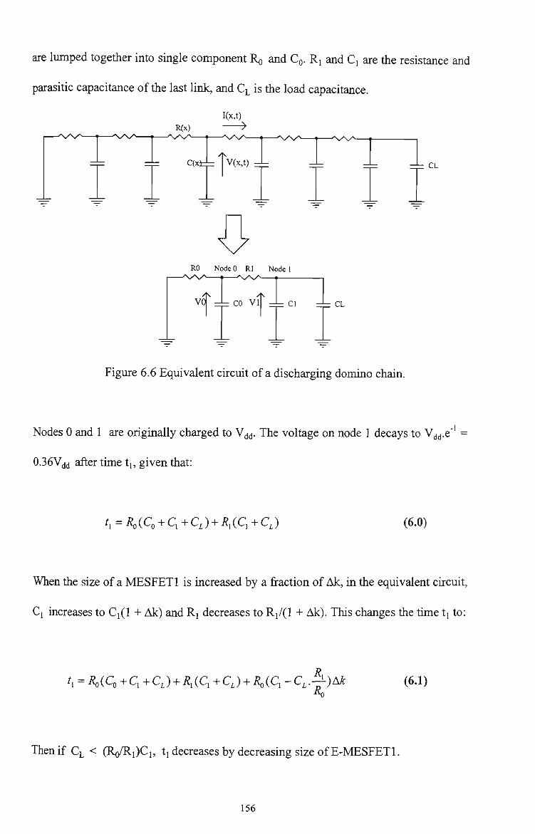
are lumped together into single component RQ and CQ. RI and Cj are the resistance and
parasitic capacitance ofthe last link, and CL is the load capacitance.
I(x,t)
R(x) • —^^/\/'' m ' % / \ / ^ » > S / \ ^ - ^ - « . ^N^/S/N m—^\y\/\
C(xi Tv(x,t) =L _L _L __ CL
\7 RO NodeO Rl Node 1
—T 'V/V^^—t——
'f CO VI iT^Lc] :=- CL
Figure 6.6 Equivalent circuit of a discharging domino chain.
Nodes 0 and 1 are origmally charged to V^j. The voltage on node 1 decays to V^ .e"' =
0.36Vd(] after tune ti, given that:
t,=R,{C,+q+C,) + R,{C,+C,) (6.0)
When the size of a MESFETl is increased by a fraction of Ak, in the equivalent cfrcuit,
Cl increases to Ci(l + Ak) and Rj decreases to Ri/(1 + Ak). This changes the time ti to:
t,=R,{C,+Q+C,) + R,(C,+C,) + R,{C,-C,.^)Ak (6.1)
Then if CL < (Ro/Ri)Ci, tj decreases by decreasing size of E-MESFETl.
156

It can be concluded that it is advantageous to design a domino or multiple-output
domino GaAs MESFET gates with large MESFETs, so tiiat tiie loading of the output
node is insignificant and the graded scaling technique is effective in the reduction ofthe
delay time. This technique of scalmg of MESFETs is particularly usefiil in very
complex gate stmctures such as Carry Lookahead Generator in Carry Lookahead
Adders.
6.2.2 Carry Lookahead Generator - Case Study One
6.2.2.1 Introduction
As the demand for higher performance VLSI processors with increased functionality
grows, there is a continuing need to improve the performance, area efficiency and
fimctionality of the arithmetic unit contained within them. Since high-speed arithmetic
circuits predominantly use Carry Lookahead Adder (CLA) stmctures, one of the
challenges in VLSI design is to stmcture multi-level CLA circuits without limiting the
fimctional flexibility. Another more fundamental challenge is to explore circuits
techniques which can exploit the performance of the CLA stmcture and yet minimise
tiie inherent complexity involved. In this section, the design and performance of a carry
generating circuit for a CLA is presented. The Carry Lookahead Generator (CLG)
circuit was implemented with GaAs MESFETs using domino and multiple-output
domino techniques and their relative performances are discussed.
157

6.2.2.2 Adder Structure
Figure 6.7 shows the stmcture of an eight-bit Carry Lookahead Adder. It consists of
two types of basic units. The first is a four-bit unit which produces the propagate and
generate terms (p; and gj) from the data a^ and bj as well as the sum output Sj. The
second unit produces the four-bit group propagate and generate terms (Pj and G;) and
all the carry bits (Ci to C4). The beisic idea behind Carry Lookahead addition is to
produce the carry signals directly from the inputs. The linear growth of adder carry-
delay with the size ofthe input word for an n-bit adder can be improved by calculating
the carries to each in parallel. The carry, Cj, and sum, Sj, for the / stage can be
expressed as:
Q=gi+PiQ-r (6-2)
where g, = a,i),
and p.=ai@bi
S,=a,@b,@q_, (6.3)
= Pi®q_,
The signal p; indicates that a carry will propagate through bit position /. The signal gj
indicates that a carry is generated directiy from the bits at position /. The carry signals
can be produced from the pj's and gj's as follows:
158

^1 — CQPQ + go
C2=CoPoPi+goPi+gi
Q = C0P0P1P2 + SoPiPi+giPi+gi
Q = C^PoPlPlPi + goPlPlPi + g^PlPs + glPi + ^3
(6.4)
(6.5)
(6.6)
(6.7)
The size and fan in ofthe gates needed to implement this Carry Lookahead scheme can
clearly become very complex. As a result, the number of stages of Carry Lookahead is
usually limited to four. The four-bit Carry Lookahead Generator module produces the
carry signals above and two additional signals group propagate, P4 and group generate,
G4. The group propagate and group generate signals are defined as follows:
and
PA = PoPiPiPs
G4 = goPxPzPi + g^PiPi + giP^ + ^3
(6.8)
(6.9)
b4-b7 a4-a7
4-bit FA
ps gs T M.S«'/N
Cs
4-bit CLG
\ / N/ Gs
Ps
C8,
bO-b3 a0-a3
4-bit FA
ps
04
T ^ U.S0-S3
Cs
4-bit CLG
Gs V ' N '
Ps
4-bit CLG
CO
Figure 6.7 An eight-bit Carry Lookahead Adder stmcture.
159

6.2.2.3 Domino Implementation of the Carry Lookahead
Generator
The carry signals, Ci to C4, of the Carry Lookahead Generator were implemented
using dynamic domino logic as shown in Figure 6.8. The stmcture includes a logic tree
and a static inverter for each output. As subsequent logic blocks are fed through this
buffer, transistors in subsequent logic blocks will be turned off during the precharge
phase. The output ofthe buffer is normally at logic low and during the evaluation phase
it is conditionally charged to logic high.
Vdd Vdd
CO-
«o—[~
• C l
Vdd Vdd
Figure 6.8 Domino implementation of carry signals of CLG.
160

Some limitations are evident from this stmcture. Ffrstly, only non-inverting outputs are
possible and secondly, in common with all dynamic logic, charge distribution can be a
problem. To overcome this problem additional precharge devices are added to the
intemal nodes of the logic free so that these nodes are also charged during precharge
phase, thus overcoming charge distribution problem. The stmcture is shown in Figure
6.9.
Additional precharge devices
Vdd
Vou
, Logic <— Blocks
^
Figure 6.9 Domino chain with precharge devices.
161

622 A Multiple-Output Domino Implementation ofthe
Carry Lookahead Generator
The carry expressions have to be fransformed to a form to enable it to be implemented
using multiple-output domino technique. C4 can be expressed as:
Q = ((((Co/?o + go) A + g^ )Pi + g2)Pi+gz) (6.10)
It can be readily seen that the first bracket defines Cj, the second bracket defmes C2,
the third bracket defines C3 and the fourth bracket defines C4 It is also important to
note that Cj is a sub-function of C2, Cj and C2 are the sub-functions of C3 and Cj, C2
and C3 are the sub-fimctions of C4 Since the overall saving in device count is due to a
reduction of replication of the sub-functions, the actual advantage of this technique
over domino logic is directly dependent on the degree of recurrence of the logic
fimctions being realised. For the carry generating cfrcuit, the expression for C4 is highly
recurrent and is most suitable for multiple-output domino implementation. The
intermediate outputs for Cj, C2 and C3 are obtained by adding precharge devices and
static inverters at the corresponding intermediate nodes ofthe logic free. Figure 6.10
shows the carry generating circuit unplemented in multiple-output domino technique.
6.2.2.5 Layout and Performance
The four-bit Carry Lookahead Generator was designed using standard domino and
multiple-output domino techniques and implemented using ISD VLSI design suite with
162

gate lengths of 0.8 micron. The layout methodology had sigruficant influence upon the
performance of the cfrcuit. Positioning of power and ground busses have significant
influence upon the performance of two cfrcuits. For example, fast transitions on signal
bus could bring about significant noise on the power bus. Thus, both the design
methodology and layout will have to address the influence of couplmg between busses
Vdd Vdd Vdd Vdd
W^ p3-
p2-
p l -
pO-
CO-
go- g l — g 2 — g 3 —
[>
O
C4
C3
C2
Cl
Figure 6.10 CLG circuit implemented in multiple-output domino technique.
on performance. The power and ground busses were placed adjacent to one another so
as to reduce thefr self inductance, and hence thefr susceptibility to current fransients.
The above circuits have been analysed and evaluated using GaAs net exfractor and
HSPICE cfrcuit simulation tools. The simulation results indicate a power dissipation of
9.444 milliwatts for a standard domino implementation and 6.044 milliwatts for
multiple output domino cfrcuit. The decrease in power dissipation is dfrectly attributed
163

to decrease in the number of devices needed to implement the CLG in multiple-output
domino technique. The average propagation delay for cfrcuit implemented using
domino technique is 0.1 nanosec whereas for the circuit implemented using multiple
output domino technique is 0.13 nanosec. The most remarkable achievement using
multiple-output domino technique is the reduction in the number of devices requfred to
implement the CLG. This technique only requires 21 devices to implement four-bit,
CLG whereas 46 devices are required for domino implementation of the same cfrcuit.
The HSPICE results for the CLG using the two design techniques are summarised in
Table 6.2.
The simulation results for the four-bit, CLG using domino and multiple-output domino
techniques are shown in Figures 6.11 and Figure 6.12 respectively. VINl, VIN2, VIN3,
VIN4 and VIN5 represent CQ, CJ, CJ, C3 and C4 respectively. The power waveforms
illusfrates the power dissipated by the four-bit, CLG implemented using the two
techniques.
T
AT I TflN TL
20.OM r
1 5 . O M t
1 0 . OM
5 . OM
1 . 2 5 0
1 . 0
7 5 0 . OM 5
5
2 5 0 . DM r
0
f ^ . ...;
0 0 . 0 M p ? y :
. 1 . . .
2 . ON T I M E C L I N 3
. L . J . .
3 . ON
— D O M C L S t - P O W E R I A
- OOnCLft'f — V i m
- A
— V lUf Z Q
^mmm^jn?. 5 . ON
Figure 6.11 Performance of a 4-bit CLG implemented in domino technique.
164

T
WOL
A T I
T f lN
TL
1 2 . OM
1 0 . OM
8 . OM
8 . OM
1 . OM r
2 . OM r
0 . ~
1 . 2 5 0
1 . 0
7 5 0 . Of
5 0 0 . DM r r
2 5 0 . O M ~
0 . ~
,4
_^ MDOMCLf lH
- POWER
: &
V
t . J . .L . J , . 1 . . I . J , . I . J . .1 . . . . . . . J . . 1 . . I . . 1 . . I . J . . f . . J . . 1 .
J _ J • " ' L
- A-
MDOMCLfll VINl
VIN2
1 .ON 0 .
I . .1. . I
2.DN TIME [LIND
•k_
•- VIN3 - Q
— VINM I *
.- VIN5
. I . J . .1. . I . .1.
3 . ON M . OM 5. ON
Figure 6.12 Performance of a 4-bit CLG implemented ui multiple-output domino
technique.
6.2.3 Conclusions - Parti
The principle behind multiple-output domino technique is to utilise the sub-fimctions
available in the logic free ofthe domino gates. Multiple outputs are available by adding
precharge devices at the corresponding intermediate nodes ui the logic tree. Since
nodes, intemal to the logic free, are being precharged for functional purposes, multiple-
output domino logic is considerably less susceptive to charge sharing than domino
logic. Because the saving in the circuit area is mairtiy due to a reduction of replication
of sub-circuits, the actual advantage of this design technique over domino logic design
technique is dfrectly dependent upon the number of recurrence in a logic fimction being
realised.
165

Table 6.2 Performance comparison for four-bit Carry Lookahead Generator
using domino and multiple-output domino techniques
Description
Number of devices
E-MESFET
D-MESFET
Gate length
Propagation delay
Cl
C2
Cs
C4
Rise time
c, C2
C3
C4
Fall Time
Cl
C2
C3
C4
Power dissipation
Domino
Technique
46
38
8
0.8 micron
0.1006 nsec
0.1012 nsec
0.1021 nsec
0.1029 nsec
0.1298 nsec
0.1382 nsec
0.1592 nsec
0.2171 nsec
0.0807 nsec
0.1172 nsec
0.1618 nsec
0.2174 nsec
9.444 mW
Multiple-Output
Domino technique
21
13
8
0.8 micron
0.1336 nsec
0.1338 nsec
0.1366 nsec
0.1398 nsec
0.1779 nsec
0.1958 nsec
0.1972 nsec
0.1924 nsec
0.1032 nsec
0.1040 nsec
0.1019 nsec
0.0941 nsec
6.044 mW
The improvement in performance is due to a reduction of load capacitance for a given
logic stage. This results from less overall device count and less parasitic wiring
capacitance as a consequence of a smaller overall layout. This also leads to lower
166

power consumption. The performance of multiple-output domino is fiirther improved
by graded scalmg ofthe MESFETs in the logic tree.
The performance advantage of this design technique over dynamic domino technique
has been demonstrated via the implementation of a four-bit CLG for a Carry
Lookahead Adder. The multiple-output domino technique demonstrates increased
circuit performance, reduced circuit area and power dissipation when compared with
the domino technique. This is due to the reduction ui the parasitic capacitance and
output loading. The most remarkable achievement using this technique is the reduction
in the number of devices required to implement the CLG.
167

Part n Static Design Technique
6.3 Merged Logic Design Technique
Static VLSI circuits are usually designed using one of the normally-off techruques
described in Chapter 4, namely, DCFL, SDCFL or SFFL techniques. DCFL design
technique is simplest and fastest of the static logic classes, but it suffers from several
shortcomings. The most noticeable being the degradation of logic voltage swing with
increasing fan out and very low noise margin (100 mV) [115]. This is due to the output
voltage being linuted by the barrier height of the MESFETs' Schottky diode at the
input ofthe next DCFL stage (650 mV). Other limitations mclude the sensitivity ofthe
gate delay to fan in, fan out and load capacitance, and the small temperature stability
margin ofthe basic gate [106].
SDCFL design technique, as the name implies, consists of a DCFL stage and a source-
follower buffer. The voltage levels at the input and the output are DCFL compatible. In
contrast, the SFFL design approach precedes the DCFL stage with a source follower as
a buffer at the input.
The Merged logic approach' to circuit design combines dfrect coupled MESFET logic
(DCFL) witii source follower DCFL (SDCFL) and source follower MESFET logic
(SFFL) so that the advantages of each logic class are exploited and circuit performance
This work was carried out in collaboration with the researchers at the Centre for GaAs VLSI Technology.
168

is achieved which is superior to that obtained from different design approaches. In the
Merged logic static design approach, shown in Figure 6.13, DCFL is predominantiy
used to achieve higher packing density and improved cfrcuit performance [116].
SDCFL technique is used to drive large capacitive loads and reahse the And-Or-Invert
(A-O-I) functions while SFFL is used to implement large fan out. In this way
significant performance improvement can be achieved. The performance of different
logic classes have been evaluated in terms of noise margin, power dissipation, fan in,
fan out and average transition times and are summarised in Table 6.3.
V
j \
dd
1 1
V
L
dd
1 1
T:
V
d dd Vdd
L
DCFL
SDCFL
SFFL
Merged Logic
Figure 6.13 Merged Logic Design Approach.
It is evident from the results that with increasing fan out the performance of DCFL
circuit is degraded. This is due to the reduced ability ofthe D-MESFET to drive the E-
MESFET of tiie fan out load.
169

Table 6.3 Performance of optimal DCFL, SDCFL and SFFL inverters
Description
Power (|i Watts)
Fan out = 1
Fan out = 3
Noise Margin (nulliVolts)
Fan out = 1
Fan out = 3
VHIGH (milliVohs)
Fan out = 1
Fan out = 3
VLOW (millivolts)
Fan out = 1
Fan out = 3
tphi (picosec)
Fan out = 1
Fan out = 3
tpih (picosec)
Fan out = 1
Fan out = 3
Logic Classes
DCFL
200
220
100
80
650
600
100
120
70
150
30
70
SDCFL
590
600
200
150
700
650
20
100
90
160
70
170
SFFL
650
660
350
300
750
610
100
100
80
120
80
110
VfflGH and VLOW ^^ the output high and low voltages respectively, and tpy and tpu, are the
propagation delays high-to-low and low-to-high respectively.
The fan in capability ofthe DCFL is restricted by the drain to source leakage current of
tiie E-MESFET, which when multiplied by tiie fan in, reduces VHIGH- The SDCFL
demonsfrates its ability to drive capacitive load significantly faster than DCFL as
170

highlighted in Figure 6.14. The fan out of SDCFL is limited by the ability ofthe D
MESFET of the source follower to discharge the gate capacitance of the following
stages, which can be significant. The SFFL class of logic has the ability to drive large
fan out. Figure 6.15 shows the fan out performance of SFFL inverter. SDCFL and
SFFL circuits dissipates more power than the DCFL cfrcuit. This is because of the
larger number of devices required to implement these circuits.
10 -r 15 20
Capacitance (fF)
•SDCFL Delay
•SDCFL Trans
-DCFL Delay
-DCFL Trans
30
Figure 6.14 Capacfrive load performance of SDCFL inverter.
The Merged logic approach to circuit design is the natural progression from
comparative studies of DCFL, SDCFL and SFFL cfrcuits. This approach involves
identifying critical parts ofthe circuit where SDCFL and SFFL techniques can be used
to improve circuit performance, such as using SDCFL stage to drive large capacitive
loads and SFFL stage to implement large fan out.
171

•SFFL Delay
-SFFL Trans
-DCFL Delay
-DCFL Trans
Figure 6.15 Fan out performance of SFFL inverter.
6.3.1 Power Series Evaluator - Case Study Two'
6.3. LI Introduction
In real time signal processing, there often exists a need for a very fast signal evaluators.
A power series evaluator is an example of a type of processing element (PE) that
performs a reasonably complex fimction. Although the architecture decided for the
implementation of this particular power series evaluator is by no means the only
approach, however, it works reliably and with minimum chip area. An important aspect
of the design methodology is the need for both top-down and bottom-up approaches.
Top-down design approach is necessary to allow the behavioural description to be
realised correctly and the bottom-up design approach is needed to ensure that the
This work was carried out in collaboration with the researchers at the Centre for GaAs VLSI Technology.
172

design algorithm chosen to unplement the processing element is such that it can be
readily mapped into GaAs, and fiirthermore, is consistent with the accepted design
principles and limitations ofthe technology.
Merged logic design approach was chosen for the implementation of the power series
evaluator. The choice is based upon the favourable properties of this design technique,
namely, high noise margins, good temperature stability and good fan in and fan out
capabilities.
6.3.L2 Behavioural Model
The general representation of an « order polynomial is given by:
y{x) = a„x"-\-a„_^x" +...-\-a^x + aQ (6.11)
To evaluate this polynomial it is necessary to fransform it into a bit-serial form so that
it can be mapped into GaAs technology. The general form of a polynomial can be
rewritten as [115]:
y(x) = {{..(a„x-\-a„_,)x + a„_2)..)..)x + aQ (6.12)
To evaluate points on the curve, it is necessary to perform n multiplications and «
additions. Implementing multiplication algorithm consumes a large amount of substrate
area and thus leads to excessive power dissipation and high fabrication costs. However,
173

by examining the polynomial, it is possible to transform it into a form in which the only
operation necessary for the evaluation of any point on the curve is found by the
application of a recursive addition process. The decomposition of a polynomial into a
recursive structure can be expressed in the Taylor's series form as:
yix,+h) = y{x,) + hy'{x,) + (f^)y"{x,)+...H^)y''(x,) (6.13)
2! «!
where XQ is a value of x for which the derivatives y',y",,..y" exist, and h = (x- x^)
Equation 6.13 can be rewritten as:
y(x^ +h) = y{x^) + d, (x^) (6.14)
where d,(x,) = hy'(x,) + {^)y"{x,)+...H^)y"{x,) (6.15) z! ni
The polynomial is reduced to a recursive set options by iteration of this process as:
d,{x,+h)=d,{x,) + hdl{x,) + {^)dl{x,)+...+{!^)d:(x,) (6.16) 2! ni
d, (xo +h) = d, (Xo) + 2 (^0) (^ -1^
where d,{x,) = hd[(x,) + {^)d[{x,)+...+(^)d",(x,) (6.18) 2! n\
The process can be continued until the fust derivative is zero. The polynomial can be
rewritten in the new form, as:
K^,>i) = > ( ,) + ,(^,) (6-19)
174

^2U,>l) = ^2(^,) + ^3U)
(6.20)
(6.21)
d„.,(Xi,,) = d„_,(x^) + d„(x^) (6.22)
(6.23)
where x,+, =Xj+h
From the transformed expression it can be seen that the processing element can
calculate any point on the curve from the irutial starting point y(Xi), usmg tiie step size,
h, with application of a recursive addition process on the individual bits of both the
initial point and a set of previously calculated coefficients, dj, d2, .... , dn. Figure 6.16
shows the logical architecture in the mapping process.
The required functional blocks to realise the algorithm are simply adders and registers.
The adders perform the calculations and the registers initially store the coefficients, and
then store intermediate values as each block is clocked during the execution cycle.
d(ii) Gin d(n-l)i Cin d(n-2)i Cin Yi
di
r^
4 REG
Cout
Figure 6.16 Block diagram of a bit-serial power series evaluator [115].
175

6.3.1.3 Physical Description
A single PE cell is shown in Figure 6.17. It consists of an adder, a register and two-to-
one multiplexer connected in such a way so that the input to the register is selectable
between the A input to the adder, and the S output ofthe adder. A single PE cell can be
cascaded horizontally to increase the order of the polynomial, n, and cascaded
vertically and pipelined to increase the bit size. The initial starting point coefficient are
loaded into the system and stored in the registers. This is achieved by the inclusion of a
two-to-one multiplexer, so that when coefficients are being loaded into the system, the
adders are by-passed and no execution takes place. Witii the addition of this
requirement the system has two modes of operation, namely. Load and Execute.
Depending on the state ofthe control input, Lj, either
(a) the system passes constant values through the register (register uiput
equals A, the input ofthe adder), i.e loading the data coefficients, or
(b) the system executes an evaluation cycle and produces a result (register
mput equals S, the output ofthe adder).
The Q output of tiie register is connected to tiie B mput of tiie adder, to realise tiie
feedback path and hence the recursive property ofthe cell.
176

C(iJ) Ld
A(iJ)-
^ MUX REG
B(iJ ' J H ^
S(ijj -^A(i
C(ij+1)
Figure 6.17 Processing element cell structure.
6.3.1.4 Adder
Addition is the most common arithmetic operation performed by any digital signal
processing system. Since the class of logic that has been decided upon for the
implementation ofthe circuit is the Merged GaAs logic, it is necessary to transform the
expressions for sum and carry into a form which contains ortiy OR and NOR gates. The
following expressions describe the sum and carry for the adder:
Sum = (A-tB-hC) + {A + B + C) + {A + B-\-C)-\-{A + B-i-C) (6.24)
Carry=(A + B)-{-(A-\-C) + {B + C) (6.25)
Figures 6.18 shows the logical representation ofthe single-bit adder cell. Appendix F
presents the design of a single-bit adder cell.
177

Can
Figure 6.18 Logical representation of a single-bit adder cell.
6.3.1.5 Edge-Triggered Register
Edge-triggered registers are designed so that they ortiy change thefr states based on
input conditions at either the rising or the falling edge of the clock. The rising of the
clock triggers a positive edge-triggered register and the ttailing edge of the clock
triggers the negative edge triggered register. Any change in the input values after the
occurrence of the triggering edge will not bring about a state transition of these
registers until the next triggering edge.
The register structure chosen for the processing element is, by necessity, an edge-
triggered device. The data at the inputs would be changing while the data at the output
is still needed for the next cell to the right. Therefore, ttansparent latches carmot realise
this property without placing severe consfraints on the clocking strategy. Figure 6.19
shows the negative edge-triggered register built out of six cross-coupled NOR gates.
This structure is suitable for the implementation of the register by the GaAs Merged
logic design techruque. As can be seen from the timing diagram in Figure 6.20, after
tiie frailing edge ofthe clock pulse, either W or Z becomes one. Note that the total time
178

required for the output transition to occur is three gate delays after the trailing edge of
the clock.
Figure 6.19 Negative-edge triggered register cell.
Clock
X = D' • clock
Y = D • clock
W
I I • •
' s ' 6 ' 7 '%
Figure 6.20 Timing diagram for the negative edge-triggered register cell.
6.3.1.6 Multiplexer
Multiplexing is the process of channelling information from one of several sources to a
single destination. A multiplexer (selector) is thus a switch connecting one of its
179
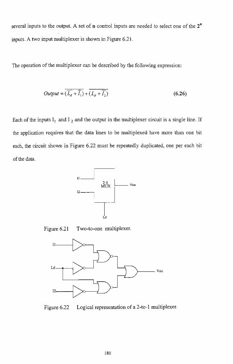
several inputs to the ou^ut. A set of n control inputs are needed to select one ofthe 2"
inputs. A two input multiplexer is shown in Figure 6.21.
The operation ofthe multiplexer can be described by the following expression:
Output = {L^+f) + {Lj + l2) (6.26)
Each ofthe inputs Ii and I 2 and the output in the multiplexer circuit is a single line. If
the application requires that the data lines to be multiplexed have more than one bit
each, the circuit shown in Figure 6.22 must be repeatedly duplicated, one per each bit
ofthe data.
Vou
Figure 6.21 Two-to-one multiplexer.
11-
Ld-
12-
Vou
Figure 6.22 Logical representation of a 2-to-l multiplexer.
180

6.3.1.7 VLSI Layout
Each smgle-bit power series evaluator cell, containing an adder, register and
multiplexer, was designed using Merged GaAs logic design technique. The cell was
implemented using Integrated Silicon Design VLSI design suite. The individual cells
were designed using the rmg notation approach [106]. The flow plan for the
implementation ofthe single-bit evaluator is shown in Figure 6.23. It encompasses all
the necessary design criteria, including placement ofthe input and output signals so the
cell can be assembled with minimum length routing paths between cells. The logical
representation ofthe cell is shown in Figure 6.24.
C(k-l)
Ak- -r: Bk 1—^
Mtrx
y Power and V - ground busse
REG :r->Q
Ck
Figure 6.23 Floor plan ofthe power series evaluator cell.
The placement of power and ground busses adjacent to each other reduces thefr self
inductance, and hence their susceptibility to current transients. From the results of
coplanar strip line and coplanar waveguide models, the inductance ofthe power busses
181

is reduced by a factor of two to three when the supply rails are placed in the proximity
of one another [ 106].
Figure 6.24 Logical representation of power series evaluator cell.
In the layout, the adder occupied seven rows of gates, register occupied four rows and
the multiplexer occupied two rows with a total of 127 GaAs MESFET depletion and
enhancement type devices. In the layout ofthe power series evaluator cell arrangement,
shown in Figure 6.25, the clock, inputs and outputs, and the conttol signals are
separated from the ground and power supply rails. This is due the high level of
crosstalk and capacitive effects which infroduce noise into the supply rails when there
are high speed switching fransients on signal lines in the proximity ofthe supply rails.
182

6.3.1.8 Simulation and Performance
The individual fimctional cells were analysed and evaluated using GaAs Net Exfractor
and HSPICE cfrcmt simulation tools. The sunulations results are summarised m Table
6.4.
The HSPICE simulation results obtamed using HSPLOT for adder, register and two-
to-one multiplexer are presented ui Appendix F. From tiie results fr can be seen tiiat tius
design approach gives large logic level swings resulting in excellent noise margins.
This design approach also allows large fan out.
GNild GMrCk
Figure 6.25 VLSI layout of a power series evaluator cell.
The performance of a single power series evaluator cell is summarised in Table 6.5 and
tiie simulation results are presented in Figure 6.26, where VINl, VIN2, VEN4, VIN5,
VIN7 and VIN8 represent tiie data input A, multiplexer (Id) confrol, clock, Q, Sum and
Carry outputs respectively. The propagation delay for each cell in the horizontal
manner is 1.48 nanoseconds. In tiie vertical dfrection fr is necessary to examine the
propagation delay of tiie carry signal. Since during each evaluation cycle tiie data is
183

moved from one cell to its intermediate right neighbour, the horizontal delay is
independent ofthe polynomial order whereas the vertical delay depends upon the entfre
bit-depth of the array. The carry signal must propagate through the entfre bit-depth of
the array and allow the adder output data to settle ui the most significant bit
Table 6.4 Performance of adder, register and multiplexer
Description
No. of Devices
E-MESFET
D-MESFET
Gate Length
Propagation delay
Sum
Carry
Q Out
Rise Time
Sum
Carry
Q Out
Fall Time
Sum
Carry
Q
Out
Power Dissipation
Noise Margin
Fan out
Adder
80
48
32
0.8 micron
0.8787 nanosec
0.5635 nanosec
0.3114 nanosec
0.3117 nanosec
0.1113 nanosec
0.1315 nanosec
12.19 milliwatts
0.37 Volts
3
Register
32
20
12
0.8 micron
0.4227 nanosec
0.2106 nanosec
0.2162 nanosec
5.362 milUWatts
0.35 Volts
3
Multiplexer
15
9
6
0.8 micron
0.1808 nanosec
0.1495 nanosec
0.1366 nanosec
2.229
milliwatts
0.35 Volts
3
184

Table 6.5 Performanceof a single bit power series evaluator
Description
No. of Devices
E-MESFET
D-MESFET
Gate Length
Propagation delay
Q (load)
Q (execute)
Carry
Rise Time
Q Carry
Fall Time
Q Carry
Power Dissipation
Fan-out
Noise Margin
Max. Clock Freq.
Power Series Evaluator
127
77
50
0.8 micron
0.6035 nanosec
1.4822 nanosec
0.5635 nanosec
0.2482 nanosec
0.3357 nanosec
0.5291 nanosec
0.2011 nanosec
17.71 milliwatts
3
0.36 Volts
1.8 GHz.
(MSB) cell before the MSB cell can be clocked. From the results the carry delay for
single cell is 0.5635 nanosec. Therefore, the MSB can ortiy be clocked after (n-1) times
this delay plus the horizontal delay of the cell for a «-bit deep array. As the bit depth
increases the horizontal delay contributes relatively less to the overall delay. For large
n, this figure can be high resulting in very slow clocking speed.
185

One possible solution to overcome the time complexity ofthe array being proportional
to the bit depth is to replace the ripple through carry adder with a Carry Lookahead
Adder structure. This will greatly reduce the carry propagation delay thus improving
the clocking frequency. The data load cycle will have considerably less delay since no
carry signal is required and furthermore, the adder is bypassed resulting in very fast
load cycle as compared with execution cycle. The maximum clock frequency of a
single bit cell during the load cycle is 1.66 GHz and during the execution cycle is 676
MHz. The single bit power series evaluator ceU dissipates 17.71 milliWatts of power.
The circuit has a large voltage swing resulting in very good noise margin and also can
drive large fan-out.
V L 0 I L M
V L 0 I L N
V L 0 I L N
V L 0 I L M
V L 0 I L N
V L 0 I L N
500 . OM
_ i I I i _
500 .OM ~
0. ~
500 .OM f
0. ~ B—
500.OM r
0. -
500. OM
0.
500.DM
I . . 1 . . I . J . I I ' I I u
-J t I L. ) . . ! . . 1 I I I I L
.5 POLTEVfl - V I N l
..,..L.J....J ^
, I
_5 POLYEVfl Z V I N 2
..J
2 P O L Y E V A
; viNH
4^
-^..ir^ 4r^ . I. . I . .1; / l . .1. . U
.JL P O L T E V A ; VIN7
r ^ ^
I . J. NI I 1— i^ . J . . I . J . .1. N L i . -^ • . i ' ^ J . . I - J
POLYEVA VIN5
POLYEVA VIN8
0. 1 . j . i l j I i I . l i I 1 I I J~
5 . ON 0.
?,i i . I I . I I .1 . I I .1 1 . . 1 , I i 1 — ^
1 0 . O N 1 5 . O N 20 .O.N 2 5 . B B W E R TIME [ L I N : 2 5 . 0 ^
Figure 6.26 Simulation result for one-bit power series evaluator. VINl, VIN2, VIN4, VIN5, VIN7 and VIN8 represent the data input A, multiplexer Id control, clock, Q, Sum and Carry outputs respectively.
186

6.3.2 Conclusions - Part II
The Merged logic approach to cfrcuit design combines dfrect coupled MESFET logic
(DCFL) with source follower DCFL (SDCFL) and source follower MESFET logic
(SFFL) so that the advantages of each logic class are exploited and cfrcuit performance
is achieved which is superior to that obtained from different design approaches.
The Merged logic approach to circuit design is the natural progression from
comparative studies of DCFL, SDCFL and SFFL circuits. This approach mvolves
identifying critical parts of the circuit where SDCFL and SFFL techruques can be used
to improve circuit performance.
The performance of Merged logic design approach is illustrated with the design and
implementation of a power series evaluator chip. From the performance analysis it can
be seen that this design approach demonsfrates excellent performance with large logic
swings resulting in excellent noise margins and large fan in and fan out capabilities.
187

Chapter Seven
Data Converters and Overcurrent
Protection Relays
7.0 Chapter Overview
In this chapter the following topics are discussed:
(i) principles of analog-to-digital conversion, and
(ii) principles of overcurrent protection relay.
Part I Principles of Data Conversion
7.1 Introduction
Most physical signals are continuous in both time and amplitude. Transducers such as
thermocouple produce continuous electrical signals (voltages or currents) that are
analogous to physical variables. To process this analog signals using digital systems,
the signals need to be converted so that they are discrete in tune and amplitude. The
188

mterfacing between continuous, analog signals and discrete, digital signals requfre
analog-to-digital conversion ofthe data.
Data converters are one of the largest sectors of linear integrated circuits. With
information processing technology becoming digital to the greatest possible extent,
analog-to-digital converters (ADC) and digital-to-analog converters (DAC) are the core
of a data acquisition system, operating as a peripheral to a data processing computer.
Although much work has been performed on the design and implementation of silicon
data converters [27 - 30], and many commercially available monolithic data conversion
circuits exist, many system applications in the areas of instrumentation, signal
processing and telecommunications requfre performance levels even higher than what
is available today in silicon. GaAs data conversion circuits are aimed at addressing
these applications with very high performance requirements.
7.2 Data Conversion Circuits
The design and implementation of an ADC is confined to linear cfrcuit m which the
digital signal is directly proportional to the amplitude of the analog signal. Nortiinear
ADCs are special circuits, offering high signal-to-noise ratio at low signal levels, and
are used primarily in telecommimication applications.
The data conversion process can be described by the following expression [73]:
189

Va=K^ib,.2-' +b,2-'+ +b„_,2"-' +b„.2") (7.0)
which can be applied to both analog-to-digital and digital-to-analog conversions. In the
former case, the analog voltage V^ is converted into a n-bit binary number. Vref is, in
this case, the high logic level ofthe system.
For digital-to-analog conversion, the inputs bj, b2,....bj, is converted into an analog
voltage by the scaling factor V f, which represents a reference voltage. The accuracy of
Vfgf is cmcial in obtairung the required resolution for the conversion. According to
equation 7.0, the conversion resolution is 1/2 LSB (least sigruficant bit) resulting m a
quantisation error of dV , where
^K=K,y.2-^"''^ (7.1)
The sampling of V^ in analog-to-digital conversion introduces another error due to the
time involved in performing the sampling. The error SjVa is given by
S7. = r ^ ^ > ^ dt (7.2)
where ta is the sampling time of measurement.
The quantisation noise, computed using equation 7.2, can be used to define the signal-
to-quantisation noise ratio (S/QN). The S/QN is given by:
190

S .rr -rr-X ^ „ + l
QN =K-v:;-2"'' (7.3)
The above expression indicates that S/QN increases linearly witii V , having its
minimum value when V„ = V. .2 " or = 2. ^ QN
The prime parameters characterising the performance of data converters are resolution,
accuracy, and dynamic response.
7.3 Analog-to-Digital Converters
This section discusses the techniques and cfrcuits used for analog-to-digital conversion.
A variety of cfrcuit organisations may be employed in the design of an ADC. Each
architecture has particular performance characteristics in terms of speed, accuracy, and
area. The major circuit architectures used in instrument and measurement envfronment
are parallel (flash) ADC, successive-approximation ADC, charge redistribution ADC,
tracking and dual slope ADC.
7.3.1 Parallel or Flash Analog-to-Digital Converter
The parallel or flash ADC organisation employs (2° - 1) comparators for an n-bit ADC
[108]. All the inputs are compared to a certain reference voltage, which is kept constant
at each comparator. For a given input, the comparators below the input level will all
191

give an output logic high and those above that level will give a complementary logic
level. Following the comparators, the flash ADC employs an encoder to convert from a
Imear or thermometer code at the comparator outputs to a standard binary code. For
some applications, a sample and hold cfrcuit precedes the comparators. However, in
many high speed circuits, the utilisation of sample and hold cfrcuit may be difficult
due to the high input capacitance ofthe comparators that it has to drive. Figure 7.1
illusfrates a specific example of a three-bit flash ADC with quantisation level of Vref/8.
C(MSB)
A (LSB)
Figure 7.1 Block diagram of a tiiree-bit flash ADC.
The flash ADC organisation is the fastest approach to analog-to-digital conversion,
because the speed ofthe circuit is only limited by the response ofthe comparator and
the propagation delay ofthe encoder. The comparator is the most critical cfrcuit in the
flash ADC, because its speed and accuracy determine the performance ofthe converter.
192

Conversion errors are due principally to comparator resolution and uncertainty (jitter)
at the comparator outputs when both inputs are equal.
The converter with data size of more than eight-bits is very complex because of the
large number of comparators [(2" - 1) for a n-bit flash ADC)] and very complex
encoding logic. In addition, 2" precision resistors are needed at the input of the
comparators.
7.3.2 Successive-Approximation Analog-to-Digital Converter
The successive-approximation analog-to-digital conversion technique [108, 118] is
based on the functional block diagram in Figure 7.2. The comparator receives the
buffered input signal and the output from the digital-to-analog converter (DAC). At the
start of the conversion, all the bits of the successive approximation register (SAR) are
set to zero except the maximum sigruficant bit (MSB). Having the MSB set to one, the
DAC provides a voltage output that represents half the digital range of the converter.
Each approximation step takes place during a clock interval. The DAC converts the
SAR contents to analog voltage V , which is compared against the input voltage Vg.
The comparator output C is used to:
(i) retain the current bit value of one in the SAR if C is high,
i.e.Va >Vd,or
(ii) change the current bit value to zero if C is low.
193

At the start of next clock pulse, the next lower-order bit is set to one. The process of
settuig a bit to one and comparing V<i with Va is carried out ui sequence for all N-bits.
At each step, a voltage increment (or decrement) of half the magnitude of the previous
step results at the output of the DAC. Figure 7.3 shows the waveforms at the DAC
output for a given value of Vj.
By starting the SAR at the midpoint, the circuit completes the conversion in exactly N-
clock pulses regardless of the amplitude of the analog signal. This is an advantage in
applications in which the time requfred for conversion must be a constant such as in
uniform sampling.
Comparator Clock
K Digital K output
oV»
Figure 7.2 Successive approximation ADC.
The successive-approximation is the simplest analog-to-digital conversion organisation.
However, since the output bits are determined sequentially, this configuration offers the
slowest conversion time for a given technology. The accuracy of conversion is
determined mainly by the accuracy ofthe DAC, and infact the best accuracy that can be
achieved with this circuit carmot exceed the accuracy ofthe DAC.
194

'So Q
m i
noo -
lOOO
oioo
oooo _i u _ i _
O 1 2 3 4 Clock period
Figure 7.3 Waveforms at the ou^ut of a successive approximation ADC.
Another implementation of successive approxunation ADC shown in Figure 7.4. It
uses a string of resistors and an analog switching matrix. The control logic activates the
appropriate switches and causes the binary fraction of VR to be applied as V^ at each
step. For a three-bit converter shown in Figure 7.4, the MSB is initially one and the two
LSB's are zero, that is A = 1, and B = C = 0. This data combination closes switches S21,
Sio, and SQO in the path from (7/16).VR to the inverting input ofthe comparator. If the
analog input voltage Va is above V^ = (7/16).VR, the comparator output goes high. At
the next step, the confrol logic applies an input of ABC = 110 to the switches. This
results in Vj = (11/16).VR. If tiie comparator output now goes low, the next
approximation ofthe data is 101, which corresponds to V^ = (9/16).VR. At the thfrd and
last step, tiie converted result is eitiier 100 if (7/16).VR < Va < (9/16).VR, or 101 if
(9/16).VR < Va < (11/16).VR. Bipolar analog signals are converted by connecting the
resistor chain between +VR and -VR.
195

YTT A B C
Digital output
Figure 7.4 Modified successive approximation ADC [108].
For an N-bit converter, this technique requires [2 ^ ^ - 2] switches and 2^ resistors.
Thus, this technique uses a large number of components as compared with Figure 7.2.
The advantage, however, lies in the ability to implement all the elements of the
converter in a single chip using GaAs technology.
7.3.3 Charge Redistribution Analog-to-Digital Converter
Charge redistribution ADC implements the successive approximation algorithm by
using a bank of capacitors [108, 118]. Instead of a strmg of resistors, binary weighted
capacitors redistribute the charge to obtain a voltage V^ proportional to the assumed
digital data. Figure 7.5 shows the four-bit charge redistribution ADC. The cfrcuit
196

operates in three phases: sample, hold, and redistribute. During the sample phase {^^ =
1), tiie switch at the upper plates of all capacitors is connected to ground, while the
bottom plates are connected to the input signal Vj. In the hold phase ((j)i, = 1), the
bottom plates ofthe capacitors are cormected to ground, while the ground cormection at
the top plates are removed. The voltage at the top plates ofthe capacitors is equal to:
V- = -V =-V.\ (1.4)
" 'I(sampledduring ((ij) \ • /
relative to the bottom plates. The charge stored in the capacitor bank is given by:
Q = 2.V^.C (7.5)
The redistribute phase ((t)r =1), begins with digital value of 1000. In this phase the right
most capacitor in the bank is cormected to ground. The switches to the other capacitors
connect to VR or ground, depending on the bit value of one or zero. This phase takes N
clock pulses during (j), for a N-bit converter. The convergence of the digital value close
to Va is obtained by successively incrementing V- to zero. Figure 7.6 illustrates the
waveforms for converting Va in the range (11/16).VR > Va > (10/16).VR. During the
first clock in phase ^j, the maximum sigruficant bit capacitor is cormected to VR and all
other capacitors are at groimd. This gives a capacitive voltage divider with an extemal
voltage VR applied to two series capacitances of C each. Since the initial charge in the
capacitor bank is 2.Va.C, the net voltage at the inverting input of comparator is equal
to:
V- = ^-V^ (7.6)
197

1 < -msb Isb V-
Compaiator
•fs
Cdp cn.'=p CIA dp C/Zdp C/%d= ly y^\ y'\ y^\ y'\ y'\
\ H \ X \ ^ ^ -0 0 0 O — — — O ^f, + p^ I
^k + tr^t
SAR + Logic
TTTT 63 ^2 6 | fefl
Digital ou^ut
Figure 7.5 Charge redistribution ADC.
4 <t>h\
-•t
A 1
n
rn
^
v-t 1 " 0
-Va
*4 C^l High
[j 1
I
1 0 0 0 1100 1 0 1 0 1011 Final output
1011 ^
T i m e
Figure 7.6 Waveforms for charge redistribution ADC.
With input Va > (VR/2), the comparator output Co goes to logic high. At the beginning
of the next clock pulse, the confrol logic keeps the MSB at one, and digital value of
1 lOO is applied. At this value V- becomes (3/4).VR - Va, which is positive. This causes
Co to go to logic low; hence at the third clock pulse 1010 is tried. Now V- = [(5/8).VR
" VJ < 0, which makes CQ to go high. Hence, the final value tried is 1011. At the end
198

of tiie fourth clock, the digital output is 1011 or 1010, dependmg on whether Co is high
or low.
7.3.4 Tracking and Dual Slope Analog-to-Digital Converters
Figure 7.7 shows a simpler altemative to successive approximation ADC, which uses a
counter and a DAC [108]. The reference voltage VR ofthe DAC is such that V at full
scale (for the counter output of 11..11) is equal to the maximum uiput analog voltage,
Va, to be converted. Conversion begins by resetting the counter to zero at the arrival of
a new sample ofthe analog voltage, Vg. With the DAC output V^ < Va, the comparator
output is at logic high. As the stair step voltage Vj increases due to increasing counter
output, the comparator output switches to logic zero when Vj reaches Va. The counter
output now corresponds to the digital equivalent of Va within half LSB. Conversion
resolution is improved by increasing the number of bits on the counter and the DAC.
The disadvantage of this scheme is that the DAC output always starts at zero before
fracking Va. Hence the conversion time is variable and depends on the amplitude of the
analog signal Va.
Conversion time can be speeded up by using UP/DOWN counter. Instead of resetting
the counter at the beginning of each conversion, the comparator output is used to count
up or down from the previous counter value. The counter output and the DAC voltage
therefore frack tiie input voltage Va. Tracking ADCs witii UP/DOWN counters are
199

useful in low cost, low speed applications such as the measurements of slowly varying
signals from temperature transducers and sfram gauges.
JL c Start
conversion
Clock AT-bit Reset counter
i£ i j / Output
DAC
Analog y input "
r\ -ATI*- Time
I . -TLT Clock U-T^
Figure 7.7 Counter ramp ADC.
Figure 7.8 shows the dual slope converter [108]. Instead of using a DAC in the
feedback loop, this converter employs an mtegrator to integrate the analog voltage Vg
over a fixed time interval. Charge accumulated in the integrator capacitor is discharged
at a constant rate to zero. The ratio of the charging and discharging time intervals is
proportional to the digital value of Va.
Conversion in the circuit begins by discharging the capacitor C and cormecting the
SPDT switch at the input ofthe integrator to the analog input voltage Va (> 0). As the
capacitor charges, the N-bit counter is simultaneously enabled to increment from zero.
Since the charging current derived from Vg is YfR, the output of the mtegrator ramps
dovm with a slope of Vg/RC. Figure 7.9 illusfrates the output waveform for the cfrcuit
[108]. With the reference (noninverting ) voltage V+ at zero, the comparator output is
at logic high for positive Vg. This causes the counter to increment. When the counter
reaches the full count and resets to zero after 2^ clock pulses, the integrator mput is
200

switched to the reference voltage VR < 0. Since VR is negative, the accumulated charge
in C is discharged at the rate of VR/RC. The counter output is stiU high, so the counter
continues to count from its reset state. When V- reaches zero, the comparator output
switches to logic low disabling the counter. The output of the counter is now
proportional to the digital value ofthe analog input signal, W^.
V, (> 0)
V« (< 0)
op amp
SPDT Discharge
Control logic
V-
v+
Comparator
W-bit counter
Output, «r
Clock
k r ^
Figure 7.8 Dual slope ADC.
The charging time, Ti, for capacitor C is given by [108]:
7; = 2 ' ' . r (7.7)
where T is the period ofthe clock.
The output of tiie integrator, V-, reaches tiie peak value, Vp, at tiie end of Tj, given by:
V=(-^).T, (7.8)
201

During T2, C discharges from tiie initial value of Vp with a slope of ( V R / R C ) . The time
interval T2, when the comparator output switches from high to low, is given by:
Vr, V {-^-).T2={J^)T R.C ' R.C '
T2=(^).T, (7.9)
Since the counter output, n,., at the end of T2 is proportional to the tune intervals Ti and
T2, the counter output n,. can be expressed as:
«c = ( ^ ) - 2 ^ (7.10)
If |VR| = Valmax ^ couutcr output of Uj. = 2 corrcspouds to the full-scale digital value of
Va = Valmaxj id Hg < 2 is proportioual to Va < Valmax' withiu the least sigruficant count.
The resolution of this converter can be improved by increasing the size of the counter.
Although the converter features a variable conversion time, it has other advantages.
From equation 7.11 it can be seen that the conversion is independent of the tolerances
of both R and C. Ortiy the clock must be stable with time for repeatability of the
converted data. Due to inherent low pass filtering in integration, high frequency noise
at the input is eliminated. In addition, if Tj = 2^.T is chosen as a multiple of the power
line period, the effects of low frequency power supply noise is minimised. To take
advantage of the latter, however, a long integration time must be allowed. For this
202

reason, dual slope converters are usually used for converting slowly varying or noisy
signals. High accuracy digital voltmeters are built using dual slope converters.
v_.
0
T , = 2 ' ' T
V 7-2= v T ^ '
Time ,
/ / S lope=^
/ Peak voltage = - -57; 7") ^r A C
Figure 7.9 Integrator output waveforms.
7.3.5 Conclusions - Parti
The voltage comparator is the basic analog-to-digital interface device. Its output is at
logic high or low, depending on the relative voltages at its inverting and norunvertuig
inputs. By nature, a comparator quantises an analog voltage as being above or below a
reference voltage. Hence, a comparator is a one-bit ADC. Paralleling many
comparators, each with a different reference voltage, and encoding the digital outputs
of the comparators, a n-bit analog-to-digital conversion is obtained. Such an ADC,
called a flash or parallel ADC, is very fast with ortiy the propagation delay of the
comparators and the encoding logic. However, a large number of comparators ((2" - 1)
comparators for an n-bit flash ADC) are requfred.
203

For ADCs requiring long time intervals, analog signal must be sampled and held
constant during conversion. A sample and hold cfrcuit uses a capacitor to charge to the
analog voltage at the tune of sampluig. With low leakage capacitors and buffered
cfrcuitry, this charge can be held vfrtually constant during the conversion interval.
Successive approximation ADCs use n step digital approximation to obtain a n-bit
binary data. A DAC m a feedback loop converts tiie digital data and a comparator
confrols the approximation. This ADC takes n clock periods to complete a conversion.
A variation on the successive approximation algorithm uses a switch matrix or a
capacitor bank in place of a DAC.
Several other methods of analog-to-digital conversion use a counter for slowly varying
signals. In the counter ramp method, a counter is activated at the beginning of a new
analog voltage sample Va. A DAC converts the counter output and applies the
converted voltage, Vj, to the comparator. When V^ equals Va, the counter is disabled.
The conversion time depends on the amplitude of the analog voltage. An UP/DOWN
counter is used to frack the input voltage and reduce the conversion time.
A dual slope ADC uses a capacitor to integrate the analog voltage over a fixed time
period. The capacitor is discharged at a constant rate, using a reference voltage, and a
counter is run simultaneously. The output of the counter at the end of the discharge
interval is proportional to the analog voltage.
Of all the structures for ADC discussed, the parallel or flash ADC organisation is the
fastest approach to analog-to-digital conversion because the speed of the cfrcuit is
204

limited ortiy by the response of the comparator and the propagation delay of the
encoder. For this reason the implementation of the data acquisition chip will be based
on the parallel or flash ADC.
205

Part II Principles of Overcurrent Protection
7.4 Introduction
The overcurrent protective devices isolate the section ofthe power system affected by a
fault so that the remaining system can continue to operate normally. The approach to
this protection mechanism is to identify a fault current, which must clearly
distinguishable from the load current, so that the overcurrent protective device can
respond to this current quickly and discormect the affected circuit rapidly. Time-
overcurrent devices have inverse time-current characteristics to clear faults with
coordinated mirumum time delays. With this type of characteristic, the greater the fault
current the shorter the trip time.
The following sections describe the fimdamentals of inverse time current relaying,
related to transmission line protection.
7.5 Overcurrent Characteristics and Protection Practices
Overcurrent protection, which was developed some seventy years ago, is still the
cheapest and simplest form of protection widely used m the power mdustry. It operates
on the principle, that, once the predetermined fault current level is reached the relay
will operate in a predetermined time and manner. Generally, classification of these
relays are in terms of thefr time characteristic, for example, instantaneous, inverse time,
206
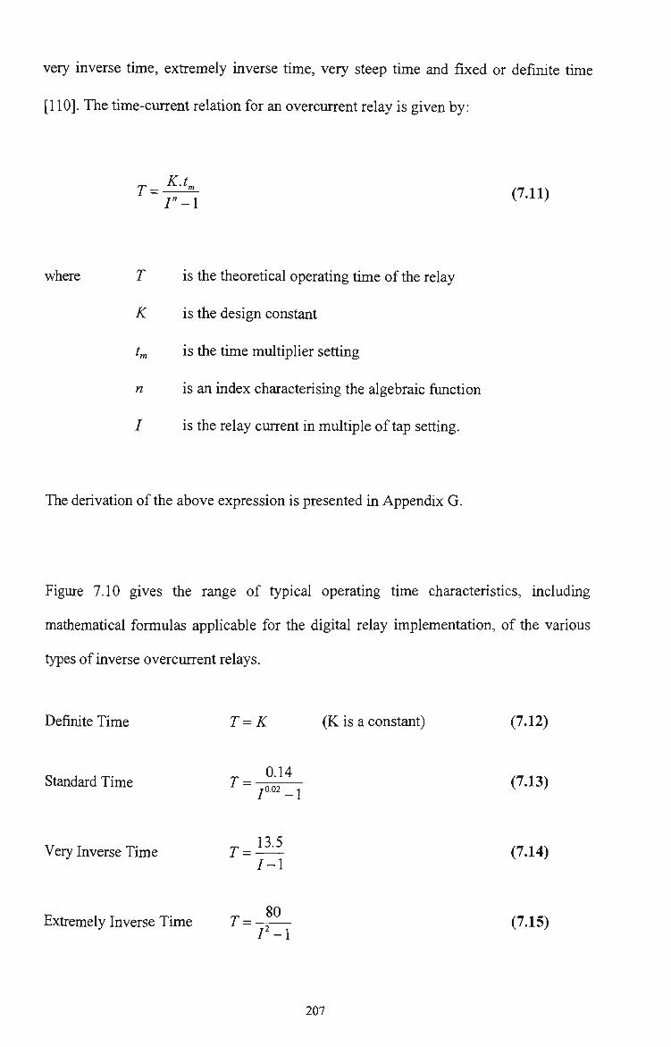
very inverse time, exfremely mverse time, very steep time and fixed or definite time
[110]. The time-current relation for an overcurrent relay is given by:
_ K.-t„
where T is the theoretical operating tune ofthe relay
K is the design constant
t„ is the time multiplier setting
n is an index characterising the algebraic fimction
/ is the relay current in multiple of tap setting.
The derivation ofthe above expression is presented in Appendix G.
Figure 7.10 gives the range of typical operating time characteristics, including
mathematical formulas applicable for the digital relay implementation, of the various
types of inverse overcurrent relays.
(7.12) Defirute Time
Standard Time
Very Inverse Time
T==K
r- 0-14 7-0.02 _ 1
r = '3.5
(K is a constant)
7-1
(7.13)
(7.14)
80 Extremely Inverse Tfrne T = - ^— (7.15)
207

operating time (seconds) 100
10
1.0
0.1
' • , 1 ^ V ' \« ' ' •* ' 1 ^v -J \\K i\
o«<
issjr ^ \
S \
V" V \
p n . * . 7
v V
v e c c
N
fe ^
K»«>
\
^ ^
N
—t-
\
. . " . ^ .
-t-^--*i 1 1 1
' 1 ' ' 1 * ' ! 1 1 1
• < I
'x 1 O^f-^^K^ * f«CO<-»tf • ^
> .
1
1 j L i 1
1
v
r ' \ ^ \
\
\
1
1 1 1
X 1
. tilt I J - ' J I J
\ ^
• I ' 1
i l l . . 1 t i l l
'! 1 ( I ' l
1 Ml 1 , , •,. 1
Current (multiple of plug setttng)
Figure 7.10 Time-current characteristics of inverse overcurrent relays.
7.5.1 Instantaneous Characteristic
The overcurrent relays having this type of characteristic operate with very small time
lag once the system current exceeds the pick-up current of the relay. The time of
operation does not change for variation in the system current above the pick-up current
level. In order to achieve the selectivity of operation among a number of such relays,
the pick-up current of each relay is set at a different level. In the power system, the
relay cormected nearer to the source has a higher plug setting. Thus, for a radial feeder,
a fault in a succeeding section, having a lower current level will operate ortiy the relay
connected to that section. However, this type of selectivity can ortiy be achieved if the
source impedance is either comparable or less than the Ime impedance. The
208

instantaneous overcurrent relay has a fiirther disadvantage, an overreaching tendency,
due to the offset current wave. In particular, for systems with high X/R ratio fr becomes
unperative to increase the time of operation to avoid overreach.
7.5.2 Definite Time-Current characteristic
In a radial feeder without any tapped connection, it is difficuh to achieve a proper
selectivity between two faults, with one occurring just before a section finishes and the
other occurring just after the next section begins. The variation of fault current under
such conditions is so small that sometimes it is impossible to set different pick-up
currents for the relays cormected to the respective sections. Under such conditions and
for conditions where instantaneous relays fail, sometime defmite tune-current
characteristic relays are used. These relays operate after a fixed interval of time after a
fault current exceeds the pick-up current level. In a radial feeder this time interval
setting gradually increases in steps for the relays cormected to sections nearer to the
source. Figure 7.11 illusfrates the defirute time-current principle. The time-current
characteristic of such a relay can be expressed as:
f.T^K (7.16)
where K is a constant.
The main disadvantage of the definite time relay lies in the fact that the most serious
fault occurring in section one is cleared after the longest time lag. Therefore, for a long
209

feeder with a large number of protection zones, the use of definite time-current relay
may become a problem because of its very slow action near the source.
©H^ Section 1 Section 2 Section 3 h-Time
lOT=K
Cuzrent
g •rl t I I
JS Discziminatin
Margin
Distance
Figure 7.11 Defirute time-current relaying techruque.
7.5.3 Inverse Time-Current Characteristic
Normally the fault current at the far end of the protected section is considerably less
than to that at the source end. The inverse time-current relay, with low operating time
for a large current, will clear a source-end fault quickly. Contrarily, its high operating
time for small fault current will allow a large time lag in clearing a far end fault. Figure
7.12 illusfrates a inverse time-current characteristic and its application in power system
protection.
It can be readily seen from Figure 7.12(b) that the fault occurring at the begimung of
the protected zone is cleared faster than the fault occurring at the end of the protected
210

zone. The relays connected to its preceding zone will respond to these faults at stiti a
slower
Time (T) sees .
I*T-Constan-K
Current i n amps (I)
Figure 7.12(a) Inverse time-current characteristic.
Dlscr i n i n a d n Margin
D i s t c i n c e
Figure 7.12(b) Power system protection using inverse time-current relays.
rate. This relay can act as back-up for the relay cormected to the succeeding zone. The
inverse-time, overcurrent relay generally provides good selectivity, but for the
following reasons its selectivity may be affected. Ffrstly, if the source impedance ofthe
system is very high compared with the protected line impedance, then the change in the
fault current levels at the begmning and at tiie end of the protected zone is not
considerable. Thus, the change in time of operation, (their ratio being inversely
proportional to the fault current ratio, is given by Zs /(Zs + ZL), where Zg is the source
impedance and ZL is the line impedance), becomes very small. Secondly, a change in
211

generatmg capacity also changes the value of the source impedance. In particular, a
sharp fall in the generating capacity increases the value of the source impedance and
thus increases the operating time ofthe relay.
7.5.4 Inverse Definite Minimum Time Characteristic
The operating time of a inverse time-current relay becomes indeterminate for very high
fault current leading to poor selectivity. Overcoming this problem, requires the
adjusting of the characteristic to have a defmite mirumum time of operation for plug
setting multiplier (PSM), higher than twenty. Thus the actual relay characteristic
becomes a inverse characteristic below this value of PSM and a straight line
characteristic above this value. In an actual relay, the operating time is fiuther
adjustable to discriminate even the mirumum operating times ofthe relays connected to
different sections of the feeder. This adjustment, known as time setting, is generally in
steps often percent (10%) ofthe maximum operation time of a particular plug settmg.
Calibration of the steps is in terms of the time setting multiplier (TSM), which is
defined as:
_ Actual operatingtime ofthe relay
Calibrated opertaing time of aparticularPSM
The standard inverse defirute mirumum tune (IDMT), characteristics are generally
shown by a family of logarithnuc curves as in Figure 7.13. The time-current
relationship for a dependent overcurrent relay can be expressed as:
212

r= K.t„
m
r-i (7.17)
For standard IDMT relay, the recommended time-current relationship is given by:
T = -0.14/ (r'-iy
Tbne in seconds
10
1.0
0.1
—s • V
\
\
— s
c- — ^ _ _ -
?^r=== „ >v« V« V. *
^ ^ ^ ^ -
^N
^ ' %
" - . - - - '^-^-^
•
—— - _ _ _ . . . . S 10 20
Multiples of plug setdng
100
Figure 7.13 Standard IDMT characteristics.
7.5.5 Extremely Inverse Characteristic
Often there is a need to protect electrical equipment against overheating. An
overcurrent relay, with its characteristic described by I T = K (an extremely inverse
characteristic) will provide such protection. The standard form of extremely inverse
characteristic is T = 80/(1 - 1). The extremely inverse characteristic for a fuses is
described by I ' T = K. Protecting rectifier transformers, a highly inverse characteristic
of I T = K is required. All these characteristics having a value of n > 2 are realised by
suitable static relays and nucroprocessor based overcurrent relays.
213

7.5.6 Very Inverse Characteristic
Standard IDMT characteristic fails to achieve good selectivity near the maximum
current levels at different substations by overcurrent relays with same TSM. The
difficulty arises in systems where the fault current rapidly decreases witii increase in
the protected length from the source. A plain inverse characteristic or its near
equivalents are more suitable in such cases. In a very inverse tune-current relays the
value of n lies between 1.02 and 2. The recommended standard for very inverse time-
current characteristic is T= 13.5/(1 -1).
Figure 7.14 compares the IDMT and very inverse time-current characteristics. The
relays come with a number of tap/plug points, each of which represents the minimum
current at which the relay starts to operate. A relay that has been set on a particular
tap/plug will begin to operate at that setting plus/minus the manufacture's tolerance. In
addition to the tap/plug setting, these relays also have a time multiplier setting. This
setting provides different operating times for the same operating current level. Figure
7.15 shows a typical family of inverse type operating time characteristics for various
time multiplier setting [110].
7.5.7 Hybrid Characteristic Overcurrent Protection
Due to increasing demand of electrical energy, power systems have become more
complex, fault levels have mcreased and fransntission margins have reduced [110].
214

Time (T) sees .
- IDMT Curve
Very Inverse
Multiples of plug se t t i ng
Figure 7.14 IDMT and very inverse tune-current characteristics.
Current MulUoIc of SctUne
Figure 7.15 Inverse time characteristics for a various time multiplier setting.
215

These conditions demand that relays used to protect power systems be more reliable,
accurate and fast compared to those used by the industry at the moment. Recent
advances in microelectronics technology have made it possible to design digital relays
to satisfy these requirements. A flexible multi-curve overcurrent protection relay
provides sigiuficantiy improved protection speed and sensitivity. Also, the fricorporated
use of defirute and inverse time overcurrent characteristics provide the hybrid
characteristics with no increase in cost or complexity to protection equipment [47].
Recently, the coordination of ground time overcurrent relay in transmission line
protection application has been proposed [45, 111]. Fundamentally, the back-up relay
pick up current must be adjusted so that each relay will operate for all faults in the
unmediately adjoirung circuits and their time setting must be just long enough to permit
the relay in the faulted circuit to operate first. This is implemented by using relays with
similar time-current characteristics, such as defirute time overcurrent relays. When the
sensed current is above the threshold setting, they operate in a predetemuned time
regardless of the magnitude of the current. Conversely, inverse time relays have very
long operating times and are often indeterminate at current magiutudes between 1 and
1.5 per unit of pick-up. To provide reasonable speed, such relays may need their pick
up setting at values lower than defirute time relays. In order to improve the protection
speed, sensitivity and security, a hybrid system incorporates characteristics of both
definite and inverse time relay. Figure 7.16 illustrates the combined use of inverse and
definite time characteristic curves.
216

Time (sees)
»•
I *
I . *
•.i
i \
V \
• k \
^ ^
•%
-
N
^
«t
C-n.
V V
\
A - <4MUM«(*SI4a)
c .
^
\
C.I. .1
A
B
c
•irtw • ^
Definite 2 sec.
Definite 1 sec.
a 4 • • • »« • « « « • • «
Plug setting on multiplier
Figure 7.16 A combined use of inverse and defirute time characteristic curves.
7.5.8 Conclusions - Part II
Overcunent protection is the cheapest and simplest form of protection widely used in
power industry. It operates on the principle, that, once the predetermined fault current
level is reached the relay will operate in the predetermined time and maimer. The
principle of various overcurrent characteristics and the development of hybrid
characteristic overcmrent protection scheme have been discussed. The combined use
of multi-curves for definite and inverse time overcurrent characteristics have been used
to significantly improve protection speed, sensitivity and security.
217

Chapter Eight
Multi-Channel Data Acquisition
Integrated Circuit
Knowledge without practice makes but half an artist.
Proverb.
8.0 Chapter Overview
In this chapter, design, implementation and performance analysis of a high speed, low
power, four-bit multi-channel data acquisition chip is presented.
8.1 Introduction
The computerised acquisition of analog quantities is becoming very important in
today's automated world. Computer based data acquisition systems are capable of
scannmg several analog inputs in a particular sequence to morutor critical quantities
and acquire data for on line use and future recall. Multi-charmel data acquisition system
usually consists ofthe following sub-systems:
218

(i) Transducers and signal conditioning cfrcuits, which senses physical
phenomena and provide electrical signals. Electrical signals generated
by the transducers must be converted into a form that the data
acquisition cfrcuit can accept. Signal conditioning cfrcuits can amplify
low level signals, isolate and filter them for more accurate and safe
measurements.
(ii) The data acquisition cfrcuit, usually consists of analog-to-digital
converter (ADC) and some sort of multiplexing cfrcuit. Multiplexing is
a common techruque for measuring several inputs with a single ADC.
The ADC samples one charmel, switches to the next charmel, samples it,
switches to the next charmel, and so on. Because the same ADC is
sampling many charmels instead of one, the effective rate of sampling
each individual channel is inversely proportional to the number of
channels sampled.
As speed is continuously increasing in elecfronic systems, especially in ADCs, data
acquisition is becoming a real issue. To perform signal acquisition at sampling rates
greater than 700 Megasamples per second (Ms/s), appropriate technology is necessary.
For a very high speed operation in a semiconductor medium, three factors become
significant, namely: carrier mobility, carrier saturation velocity and existence of senti-
insulating subsfrate. The latter property allows mixed analog and digital cfrcuits to be
implemented on the same chip. GaAs technology mostly fulfils these requfrements, and
219

together with low power dissipation, provides a technology base for a new generation
of analog and digital cfrcuits.
The four-bit multi-channel data acquisition chip is based on very fast flash ADC with
multiplexed inputs. The ADC is based on an algorithm that requfres oitiy 2 '
comparators instead of (2" - 1) comparators for a n-bit conversion. This approach, thus
reduces the complexity of multi-bit flash ADC design. The design of the proposed
ADC is module oriented, which enables multi-bit high resolution flash ADC to be
developed by cascading a number of n-bit flash modules.
8.2 Analog-to-Digital Conversion for High Speed Data
Acquisition System
Real-time data processing systems operating at Gigabit rate are primarily lunited by the
ADC performance. The fastest ADC available in practice is the flash ADC involvmg a
conversion time equal to the propagation delays of the comparator and the encodmg
logic. However, the complexity ofthe cfrcuit increases rapidly with the increase in the
number of bits. An increase of one bit in the digital output nearly doubles the circuit
complexity. For instance, when an eight-bit ADC needs 255 comparators for frs
realisation, a rune-bit ADC requires 511 comparators for its unplementation. This
increase in the complexity ofthe hardware discourages its feasibility of implementation
for bigger number of bits. Some effort has been made to reduce the comparator count
220

using pipelining technique [35, 36, 38]. This scheme generally requfres DACs,
amplifiers and other additional cfrcuitry.
In this section, design and GaAs implementation of a four-bit flash ADC and a multi-
charmel data acquisition chip are described. The ADC requfres ortiy 2^"' ' comparators
instead of (2" -1) comparators for a n-bit conversion and does not requfre complex
hardware.
8.2.1 Flash Analog-to-Digital Converter Topology
The development of this technique can be explained with reference to a three-bit flash
ADC shown in Figure 8.1 [117]. The outputs ofthe comparators and the corresponding
digital ou^uts ofthe ADC are tabulated in Table 8.1. From the table it can be seen that
the comparator which compares the analog input voltage with Vrei/2 generates the most
significant bit of the converter. This comparator output, X3, is chosen as a control
signal. When X3 is logic '0', the output of lower order comparators (X2, Xj and XQ)
determine the final ADC outputs. Sinularly, when X3 is logic ' 1 ' , ortiy the higher order
outputs of comparators (X4, X5, and Xg) determine the final outputs, because the lower
order comparators outputs are all at logic ' 1 ' . Thus, either the three lower order
comparator outputs or the three higher order comparator outputs determine the fmal
ADC output, depending upon the output value of the Vje/2 comparator. This implies
that the comparator count can be halved, if, VK^2 comparator output is used to confrol
221

a DPST switch. The two inputs of the switch or a multiplexer, coimect to the
corresponding reference voltages. Figure 8.2 shows the structure of such a scheme.
C(MSB)
A (LSB)
Figure 8.1 Three-bit flash ADC.
Table 8.1 Outputs for a three-bit flash ADC
X<;
0
0
0
0
0
0
0
1
Xs
0
0
0
0
0
0
1
1
X4
0
0
0
0
0
1
1
1
X3
0
0
0
0
1
1
1
1
X2
0
0
0
Xi
0
0
Xo
0
c
0
0
0
0
1
1
1
1
B
0
0
1
1
0
0
1
1
A
0
1
0
1
0
1
0
1
222
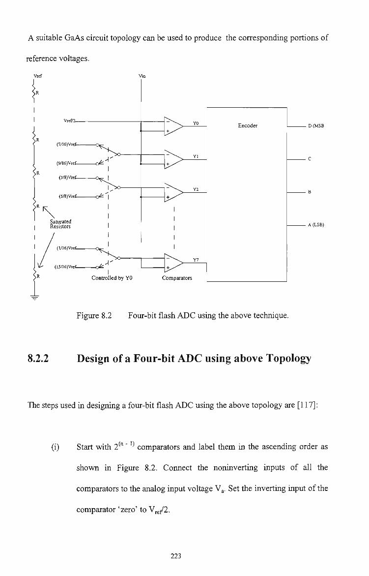
A suitable GaAs cfrcuit topology can be used to produce the corresponding portions of
reference voltages.
Vref
VTtilZ.
(7/16)Vrei-
(3/8)Vre£-
\ Saturated Resistors
(l/16)Vre£-
Vm
(9/16)Vrrf o ^ •
I
(5/8)Vre£ o ^ |
(I5/I6)Vre£ o ^ '
YO
Yl
Y2
Y7
I Controlled by YO Comparators
Encoder D(MSB
A (LSB)
Figure 8.2 Four-bit flash ADC using the above technique.
8.2.2 Design of a Four-bit ADC using above Topology
The steps used ui designing a four-bit flash ADC using the above topology are [117]:
(i) Start with 2^"" ' comparators and label them in the ascending order as
shown in Figure 8.2. Cormect the noninverting inputs of all the
comparators to the analog input voltage Y^. Set the inverting input ofthe
comparator 'zero' to Vref/2.
223

(ii) Use the output of this comparator to control the switches, which have
thefr outputs connected to the inverting input of the other comparators.
Cormect the inputs of the switches to the appropriate portions of the
reference voltages.
(iii) Encode the output of the comparators into appropriate binary values
using the truth table of Table 8.2.
Table 8.2 Relationship between comparator outputs and ADC outputs
Yo
0
0
0
0
0
0
0
0
Yl
0
0
0
0
0
0
0
1
0
Y2
0
0
0
0
0
0
1
1
0
0
1
1
1
1
1
1
Y3
0
0
0
0
0
1
1
1
0
0
0
Y4
0
0
0
0
1
1
1
1
0
0
0
0
1
1
1
1
Y5
0
0
0
0
0
0
0
0
1
1
1
Y6
0
0
0
0
0
0
0
0
1
1
Y7
0
0^
0
0
0
0
0
0
1
D
0
0
0
0
0
0
0
0
C
0
0
0
0
1
1
1
1
0
0
0
0
1
1
1
1
B
0
0
1
1
0
0
1
1
0
0
1
1
0
0
1
1
A
0
1
0
1
0
1
0
1
0
1
0
1
0
1
0
1
224

8.3 Mixed Analog-Digital Design
Mixed analog-digital cfrcuits are the largest growth area in microelectrorucs. Analog
cfrcuitry fmd wide use in systems applications such as telecommunications, consumer
products, data acquisition systems, instrumentation and measurements which need an
analog interface to an extemal environment to couple with digital signal processing
systems. Many board-level mixed analog-digital systems have begun to rrtigrate down
towards single chip implementation, containing many different parts, both, analog and
digital. That means that today's analog circuitry finds more use in ntixed analog-digital
systems than in stand alone analog cfrcuits. In digital sections of these chips important
parameters like noise are oitiy a question of digital wordlength while the analog
designers often deal with signals with near infirute levels of resolution.
The success of mixed analog-digital design relies strongly on appropriate design
techniques for implementation of these circuits. The analog cfrcuits for the multi-
charmel data acquisition chip have been implemented using Source Coupled GaAs
MESFET logic and the digital circuits have been designed using E-D GaAs MESFET
Merged logic.
8.3.1 Source Coupled GaAs MESFET logic
To realise high speed GaAs analog integrated cfrcuits a suitable design technique
should be chosen to meet the noise margin, power, speed and the interface requirements
225

witii the tolerance to fabrication process and temperature variations. The dispersion of
device characteristics through out the chip and wafer is one of the biggest problem in
reahsing integrated cfrcuits in GaAs technology. It also is a very important
consideration in comparator design. The threshold voltage of a GaAs MESFET is the
difference of the Schottky barrier voltage and the pinch-off voltage. The latter being
proportional to the square of the thickness of the active layer. This implies that the
threshold is very sensitive to geometric variations. In SCFL cfrcuitry the structure is
such that ortiy the relative variations of threshold voltages is unportant. Hence, the
input level required for switching is ortiy dependent on the difference between the
threshold voltages of the MESFETs. In most cases the threshold voltage difference
between neighbouring MESFETs on a chip is small.
The salient features of a SCFL circuit are as followers:
(i) If the FET's threshold voltage vary from wafer to wafer, the operating
point and the output voltage can be adjusted by controlling the reference
voltage.
(ii) Due to the source follower buffer, the SCFL circuits are capable of
driving many gates.
(iii) Increase in fan in reduces the transition region in transfer characteristic
and thus increases the transfer gain. The use of constant current source
prevents variations in the output voltage swing and level.
226

(iv) High input sensitivity and versatility in appHcations.
SCFL techruque seems to be the best choice in the MESFET process for a nux of
GaAs digital and analog integrated cfrcuits on the same chip, mainly because of its
wide tolerance to threshold voltage range and its immimity to temperature variations. It
also has an excellent fan out capability, a small input capacitance and a small
discharging time permitting high speed operations.
8.4 Comparator
The comparator is the most critical circuit in a flash ADC, because its accuracy and
speed determine the performance of the converter. The comparator speed has two
parameters, namely, setup time and delay time. The sum of these parameters, called
decision time, determines the time requfred by the comparator to determine a valid
logic output level for a given difference in the magnitude ofthe inputs. The resolution
of the comparator is also very important because it affects the resolution of the ADC.
Two parameters determine the comparator resolution, namely, offset and hysteresis.
Both of these parameters can be measured from the comparator transfer curve.
Hysteresis and offset determine the smallest possible voltage difference which can be
reliably sensed or resolved, and therefore the resolution that can be obtained from the
ADC. Offset matching between comparators is a major design concem in configuring a
flash ADC. The offset plus hysteresis between each comparator has to match to within
one LSB in order to avoid errors like missing codes.
227

8.4.1 Comparator Implementation
A cfrcuit diagram of a comparator using E-D GaAs MESFETs is shown in Figure 8.3.
The circuit is based on a high gain cascade SCFL structure as a switching stage and a
source follower level shifter for each output. When the input signal, Vjn, is applied to
MESFETl of the differential amplifier, the voltage Vj is compared with the fixed
reference voltage V^f applied to MESFET2. Then either, MESFETl or MESFET2 can
switch on, (in the current mode) depending on whether Vjn is higher or lower than the
reference voltage V f. The characteristics of a comparator is characterised by the
switching behaviour of differential pair. The drain current flow for the differential pair
is given by:
J _ IQ , P\(Vi„ V^^j) 2./0 2 /onx
I =Zi+MiL_Jk2 \^-(v -V ,Y (8.1)
where I^i and 1^2 are tiie dram currents for MESFETl and MESFET2
respectively,
^i and P2 are the HSPICE parameters dependent on the process and
geometry of E-MESFETl and E-MESFET2 respectively, and
IQ is the current flow through the common source.
228
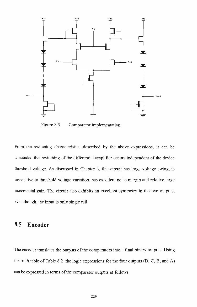
Vdd
V i n .
Vdd
VlT
J
Vdd
11 #
P
Vdd
Vref
t
Vout2
Figure 8.3 Comparator implementation.
From the switching characteristics described by the above expressions, it can be
concluded that switching of the differential amplifier occurs independent of the device
threshold voltage. As discussed in Chapter 4, this cfrcuit has large voltage swing, is
insensitive to threshold voltage variation, has excellent noise margin and relative large
incremental gain. The circuit also exhibits an excellent symmetry in the two outputs,
even though, the input is ortiy single rail.
8.5 Encoder
The encoder franslates the outputs ofthe comparators into a final binary outputs. Using
the tmth table of Table 8.2 the logic expressions for the four outputs (D, C, B, and A)
can be expressed in terms ofthe comparator outputs as follows:
229

D = Y, (8.2)
C = Y, (8.3)
B = {Y,+Y,).{Y2-^Y,).{Y,+Y,) (8.4)
A = {Y,+Y,).(Ys+Y,).(Y,+Y,).{Y,+Y,)
{Y, + Y,).(Y,+Y,).{Y,+Y,) (8.5)
where Yg, K; are the outputs ofthe eight comparators.
E-D GaAs MESFET Merged logic design technique was chosen for the implementation
of the encoder. This design methodology combines DCFL with SDCFL and SFFL to
exploit the advantages of each logic class and to achieve cfrcuit performance which is
superior to that obtained from the different individual design approaches. The Merged
logic design technique, predominantly uses DCFL to achieve higher packing density
and to improve circuit performance, SDCFL techiuque to provide drive for large
capacitive loads and to realise the And-Or-Invert (A-O-I) functions, and, SFFL to
implement large fan out. In this way, significant performance improvement can be
achieved. Increasing fan out degrades the performance of DCFL circuit because of the
reduced ability of tiie D-MESFET to drive tiie E-MESFET of tiie fan out load. The
drain to source leakage current of the E-MESFET restricts the fan in capabtiity of the
DCFL. The logicd circuit representation for the encoder, based on NOR/OR structure,
is shown m Figure 8.4. Interfacmg the analog cfrcuits, operating at 12 volts supply, to
the low voltage digital cfrcuits operating at a supply voltage of 1.5 volts, required
appropriate level shifting.
230

YO.
Y4.
D(MSB
C
Y 2 -
Y 6 -
Y2-
Y2r-
Y6-
Y5-
7 5 -
Y3-
72-
Y3.
Y5-
77-
75-
Y7-
Yl-
Y7.
77-
YI-
r
I>
r
A (LSB)
Figure 8.4 Logical representation ofthe encoder.
See Appendix H for the details ofthe encoder design.
231

8.6 Cascading Analog-to-Digital Converters
Multi-bit flash ADC can be designed by cascading a number of four-bit flash ADC
modules, for example, a four-bit flash ADC by cascading two two-bit flash modules. In
the cascaded implementation of two modules, two stages of comparison are made on
the given analog input. For an analog input voltage, V ,, lyuig in the full scale range of
0 - V Volts, the first comparison is made for the three voltage levels at V/4, V/2, and
3V/4. The most sigruficant two-bit digital outputs, D and C are determined, as in
conventional flash ADC. As a carry-over operation, the next stage of comparison is
made on the residue ofthe analog input voltage, Vj,,, from the analog equivalent ofthe
most sigruficant two-bits, producmg the least sigruficant two bits of the digital outputs,
B and A. Before making this comparison, the residue voltage is amplified four times so
as to use the same reference voltage levels for comparisons at the different stages. In
general, an amplification factor of 2" is needed for a n-bit flash module.
Figure 8.5 shows the structure of a four-bit flash module that can be cascaded to form a
multi-bit flash ADC [38]. D, C, B, and A represent the digital outputs of the flash
converter while V^ is its equivalent analog voltage. These bits (D, C, B, and A) control
the switching ofthe reference voltages V/2, V/4, V/8, and V/16 respectively to the
summing amplifier. The inverted analog input forms the fifth input of the summing
amplifier. The gain factor of sixteen is used, thus the difference voltage, V , is defined
by: {[Vin - {analog equivalent of (D, C, B, and A)}] x 16}.
232

A sixteen-bit ADC can be realised using four cascaded four-bit modules as shown in
Figure 8.6. The analog voltage of the ffrst module serves as the analog input to the
ADC. The combined digital outputs provided by the modules would form the overall
digital output ofthe ADC. The front-end module gives the most significant bits while
the tail-end module provides the least significant bits.
V i n .
Vref. ADC
16R
Va .
R
- # R
# R
R
^ — i
Switch
D(MSB)
A (LSB)
Vre£7
Vrefy4
Vref78
Vrefl6
Vin
Figure 8.5 Four-bfr flash ADC module.
D,jD,<D,jD,j D,|DioD,D, D, D, Dj D,
Vm ADC
DjDjD, Do
Figure 8.6 Cascading flash ADCs.
233

8.7 Analog-to-Digital Converter Layout and Performance
The component blocks of the four-bit flash ADC were implemented using E-D GaAs
MESFETs with gate length of 0.8 nucron. The comparators were designed using the
Source Coupled GaAs MESFET logic and the encoder was designed usmg the E-D
GaAs MESFET Merged logic design technique.
The layout methodology has sigruficant influence upon the performance of the cfrcuit.
Commurucation paths between cells and positioning of power and ground busses have
significant influence upon the performance of high speed VLSI systems. For example,
fast fransitions on signal bus could bring about significant noise on the power bus.
Thus, both the design methodology and layout will have to address the influence of
coupling between busses on performance.
The placement of power and ground busses adjacent to each other reduces their self
inductance, and hence their susceptibility to current fransients. From the results of
coplanar strip line and coplanar waveguide models, the inductance of the power bus is
reduced by a factor of two to three when they are placed in the proximity of one another
[106]. The ring notation approach, discussed in Chapter 5, exploits this advantage and
enables the designer to layout the skeleton of the cfrcuit rapidly, paying particular
attention to power and signal busses between adjacent cfrcuitry.
234

Using the above design methodology and layout approach, the cfrcuits were
implemented using ISD VLSI design suite nmnmg on Sun workstation. The VLSI
layouts for a comparator, encoder and the four-bit flash ADC are shown in Figures
8.7(a), (b), and (c).
The above cfrcuits have been analysed and evaluated usmg GaAs net extractor and
HSPICE circuit simulation tools. The simulation results indicated a power dissipation
of 11.12 mini Watts with propagation delay of 0.31 nanosec for the four-bit encoder
with a supply voltage of 1.5 Volts. The comparator, which operated from a supply
voltage of 12 Volts dissipated 17.13 mitiiWatts with the hysteresis of 0.3 Volts. Table
8.3 details the results for the four-bit flash ADC and its components.
The sampled HSPICE simulation results for the four-bit flash ADC and the components
are shown in Figure 8.8. Figure 8.8 (a) shows the simulation results for a comparator,
where VINl, VIN2, VIN3, and VIN4 represent the input voltage, vin, circuit reference
voltage, vref, comparator true and complementary outputs, outl and out2 respectively.
The power waveform represents the power dissipated by the circuit. Figure 8.8 (b)
shows the results for the encoder, where VINl and VIN2 represent the two LSBs (Z3
and Z4 respectively). The inputs to the encoder are represented by the waveforms of
VIN3, VIN4, VIN5, VIN6, VESf7, and VIN8. The power waveform represents tiie
power dissipated by the encoder cfrcuit. Figure 8.8 (c) shows the simulation results for
a four-bit ADC, where VINl, VIN2, VIN3, VIN4, and VIN5 represent tiie friput
voltage, vin, and the outputs Zl, Z2, Z3, and Z4 respectively. The power waveform
represents the power dissipated by the four-bit ADC.
235

Table 8.3 HSPICE simulation results
Description
Number of Devices
E-MESFET
D-MESFET
Diodes
Gate Length
Propagation Delay
Rise Time
Outl
Out2
Fall Time
Outl
Out2
Power Dissipation
Noise Margin
Hysteresis
Conversion Time
Comparator
31
4
7
20
0.8 micron
0.36 nanosec
0.36 nanosec
0.41 nanosec
-
0.32 nanosec
0.36 nanosec
17.13
milliwatts
0.6 Volts
-
-
Encoder
85
42
33
-
0.8 micron
0.31 nanosec
0.21 nanosec
-
-
0.17 nanosec
-
-
11.12
milliwatts
0.35 Volts
-
-
4-bit Flash ADC
333
42
89
160
0.8 micron
-
0.26 nanosec
-
-
0.28 nanosec
-
-
120.6 milliwatts
0.35 Volts
0.3 Volts
0.62 nanosec
where Outl and Out2 are the two outputs ofthe comparator.
GR-vrr auMi.
Figure 8.7 (a) Mask level layout of a comparator.
236

GM: Z4
GN: A
GN: B %: C
Figure 8.7 (b) Mask level layout of an encoder.
EH:Z1
Figure 8.7(c) Mask level layout of a four-bit flash ADC.
237

I flNCOHPl - V I N l
£:
V L 0 I L N T
V L 0 I L N T
V L 0 I L N T
V L 0 I L N r WTL fiOI _ TTN l O - O M f
Tf' Q — '• • 1 •• I • • I 1. - .1. . .1. . .1. , .1. . .1 . .L . . t . . I . . 1 . . I . . 1 . .
5 . ON 1 0 . O N 15 . ON 0 - T I M E C L I N )
ANCOMPl ^ POWER : A
20 .ON
Figure 8.8 (a) HSPICE smiulation for a comparator. VINl, VIN2, VIN3 and VIN4 represent vin, vref, true and complementary comparator outputs.
V L 10.OH 0 I L N . J . . . 1 . . . I . . .1. J . .. I .. . 1 . . .1. J . . . I ... 1. .. .1.
E N C O D E R l : POWER
J..J} ^ 10.ON 20.ON
TIME CLIN) 30 .ON 32.ON
Figure 8.8 (b) HSPICE smiulation for an encoder. VINl and VIN2 represent the encoder outputs Z3 and Z4. VIN3 - VIN8 represent the encoder inputs.
238

S O " " V L - - flDCl
^ V I N l
L K _ i . . i . . i . . I . . ! . . ! , . i - . i - . t . - l - . i . • • - • I - I - - I - • ' • • ' • • " I I I I I / . I . 1 - i . i • i - i ^
V L r : '• _r flOCi 0 I zo.on- : • • • ; i ^^^^ I N I _ l . . 1 . . ) . . 1 . . 1 . . 1 . . 1 . . 1 . . 1 . - L . l . . 1 . . 1 . . 1 . . 1 . 1 - . 1 . L - i 1 • ' • ' • I • ' • ' - ^ • > • ' - 1 - ^
V L '- :..../:....:.:.: : \ . . . : : - ftcci
I N - , . . . \ . A , , \ . , i , \ , I. t \ \ I I > \ \ \ I . I I A
V L - . / . \ . •/ : flOCl
0 I 500.OMT : • [••'.' V; ;/• = Z i i i l L N
0. Z^li ll. .1. .11 ll. -ll l O i l . -I. iL .11 .1. ll! . t . I . L . I . L . l \ I . L • 1 I I . 1 . " . 1 . 1 . 1 . 1 - 3
V L - • \ . . I. •\ - RDCl 0 1 5 0 0 . O M T V " ' ' . ' • • / • - 1 = V I N 5 L N f. Z - l . .1. - I - . I . .1. .1. .1 . .Vi i l . l l . .1. .1. .I.'>L .1 iL .L iL . i M .1 .1 .1 -1 • 1 - V . I . I • l - A
«TL lOO.OM^ : . . ^ r 7 - - t T - : - — - T X - . . . - - ^ ^ AOCl floi z : : : : - / " " ' ^ T T N - I _ i . .1. .1. .1. .L .1. .1. .1. .1. . 1 .1. .1. .1. .L - I 1. .1 - i -1 . 1 i i i • ' • ' -> • I • I • ' - j
" • 2 . S O N 5 . O N 7 . 5 0 N 1 0 . O N 1 2 . S O N 0 . TIME C L I N ) 1 5 . ON
Figure 8.8 (c) HSPICE sunulation for a four-bfr flash ADC. VINl - VIN5 represent the input voltage, vin, and the outputs Zl - Z4 respectively.
8.8 VLSI Implementation of Four-Bit Multi-Channel
Data Acquisition Chip
The four-bit multi-channel data acquisition chip, contairung a analogue comparator, an
encoder and multiplexer, was designed and implemented using Integrated Silicon VLSI
design suite. To obtain low power, high speed, good noise margin and fan out, E-D
GaAs Merged logic design techruque was chosen for digital cfrcuits. SCFL design
technique was chosen for the design of the analog cfrcuits on the same chip, mairtiy
because of: its wide tolerance to threshold voltage variation, its immimity to
temperature variations, its excellent fan out capability, its small mput capacitance and a
small discharging time (permitting high speed operations).
239

Figure 8.9 shows the floor plan for the four-bit multi channel data acquisition chip. It
encompasses all the necessary design criteria, including placement of the input and
output signals so that the cells can be assembled with minimum length routing paths
between cells. Figure 8.10 shows the VLSI layout ofthe four-bit multi channel data
acquisition chip.
Vins
Vref
Analog Interface Digital
\ - - ...
Figure 8.9 Floor plan for a four-bit multi-channel data acquisition chip.
8.9 Simulation and Performance
The four-bit multi-channel data acquisition chip was analysed and evaluated using
GaAs net extractor and HSPICE circuit simulation tools. Table 8.4 details the results
for the data acquisition chip.
Figure 8.11 shows the HSPICE sunulation results, for different input conditions, where
VINl represents tiie multiplexer confrol signal, VIN2, VIN3, VIN4, and VIN5
represent the four output bits of the data acquisition chip, and VIN6 represents the
inputs to the two channels of the chip. From the results, it can be seen that this design
240

technique gives large logic swings resulting in exceUent noise margin. The total power
dissipation for the chip is 185.6 milliWatts, uidicating the suitability of this design
technique in implementing VLSI cfrcuits.
Table 8.4 Performance of the four-bit multi-channel data acquisition chip
Description
Number of devices
E-MESFET
D-MESFET
Diodes
Saturated Resistors
Gate length
Power dissipation
Noise margin
Conversion Time
Data Acquisition Chip
397
84
138
160
15
0.8 micron
185.6 milliwatts
0.35 Volts
0.85 nanosec
8.10 Conclusions
This chapter presents the design and implementation of a GaAs VLSI ultrafast multi
channel data acquisition chip. Appropriate design techniques and technology have been
chosen for the design of this mixed analog-digital chip. SCFL techruque is tiie best
choice in the MESFET process for a ntix of GaAs digital and analog integrated circuits
on the same chip, mairtiy because of its tolerance to threshold voltage
241

BN:«T
Figure 8.10 Mask level layout of a four-bit multi-channel data acquisition chip.
V L 0 I L N
V L 0 I L N
V L 0 I L N
V L 0 I L N
V L 0 I L N
V L 0 I L N
1 . 0
0 .
5 . 0
0 .
1 . 0
0 .
J . . . I . . . I
- flOCl - V I N l - v
I .0 —
0 . ~
50 . OM f=
0 . —
5 0 0 . OM =~
0 . ~
0 .
Q .; ;. ; - flDCl .
; r V I N E • i........J...1...L.......a.......i..........^-.J»'^
..Z flOCl . ; V INS
I U 1 / . . .1. .. J.-.l . . .L . . .1. . . J. .-J ^ ^ -J I , .1 1 1 u.
, I • 1 _ — I — / . . . J... 1... I.. .>• . .1. • • J.
. - flDCl - V I N 3 ; A
WV. . I . . .1. . . .1. . . .'. -3
- flDCl '^ V I N l
a
. .1 ,... J...,.. .1.. ..I I... 1.. . 1 . . .1... .1... .'• J
2 . ON "! -OM 6 .ON T I M E C L I N )
z flDCl ; V I N S
A
8 . ON
Figure 8.11 HSPICE simulation results for a data acquisition chip. VINl - VIN5 represent the multiplexer control and the outputs of the data acquisition chip DCBA respectively. VIN6 represents the inputs to the chip.
range and its immunity to temperature variations. It also has an excellent fan out
capability, a small input capacitance and a small discharging time permitting high
speed operations. Digital components have been designed using E-D GaAs Merged
logic design technique. This concept combined DCFL with SDCFL and SFFL so that
242

the advantages of each logic class could be exploited. The cfrcuit performance achieved
using this techruque was much superior to that obtained if the cfrcuit had been
implemented with any one ofthe logic class exclusively.
Design of a flash ADC as presented, requfred ortiy 2^°" ^ comparators to implement a
n-bit flash ADC. The most sigruficant bit ofthe comparator output formed the confrol
signal for switches, which connected the appropriate reference voltages, depending on
the input signal level, to the remaining comparators. This approach greatly reduced the
complexity of the flash ADC. Depending upon the apphcation, high resolution ADC
could easily made by cascading four-bit flash ADC modules.
The multi-channel data acquisition chip needed 397 devices and dissipated 185.6
miUiWatts of power. The conversion tune was 0.85 nanosec with noise margin of 0.35
Volts. These results indicated the appropriateness of the design technology and
techniques used for rruxed analog-digital circuits on a single chip.
243

Chapter Nine
VLSI Implementation of an Eight-bit Multi-
Function Multi-Protection Relay
If all the computer companies continue to buy all their logic devices from the merchants, the uniqueness
of their computer products would disappear.
Peter R. Treiney.
9.0 Chapter Overview
This chapter describes the design, implementation and performance of an eight-bit
multi-fimction multi-protection relay implemented using E-D GaAs MESFET Merged
logic design technique.
9.1 Introduction
Modem power systems need to generate and supply high quality electric energy to the
consumers. A growing demand for accurate, selective and reliable overcurrent relays
have increased recently due to an increase in the complexity and capacity of power
systems. Advancements in digital technology associated with power industry has had
244

sfrong impact on the development of power system protection equipment and
techruques.
Computer based digital relaying techruques have been well established in many aspects
of power system protection [41, 42]. The availability of cheap and powerful
microprocessors in recent years have led to thefr increasing use in power systems
protection. Several types of microprocessors have been used to unplement different
type and level of relaying techniques. An eight-bit, microprocessor-based, overcurrent
relay was developed [109], in which Intel 8085 microprocessor was used ui the
implementation of single input overcurrent relaying system. Further research using the
same processor led to the development of a multiple overcurrent relay [42]. Recentiy a
32-bit relaying techruque for power system protection was developed [47], in which a
Motorola MC68020 nucroprocessor was used to provide a multi-fimction protection
scheme with requfred speed, accuracy and reliability.
Recent developments in microelectroruc technology, in particular the GaAs digital
technology, has led to the application of VLSI GaAs ICs in high speed, low power
relaying techniques for power system protection schemes.
9.2 Hybrid Characteristic Overcurrent Relay
The flow chart in Figure 9.1 characterises the operation of a hybrid overcurrent relaying
system for power protection. For each overcurrent protection section, a look-up table
245
stores the fault current values and the time-out delays based on time-current
characteristics described by equations 7.13 - 7.16 in Read Only Memory. The relay
monitors the magnitude of the incoming signal (phase and line currents and voltages)
via data acquisition cfrcuit ( multiplexer, signal conditioning cfrcuit and analog-to-
digital converter) and compares this with the set value stored in memory as a look-up
table. At this point in tune the timer is loaded with an appropriate time-out value and
waits for the confroller to signal the start of time-out period. If the output of the
comparator indicates that the morutored signal is greater than the set value, the
confroller starts the time out period. At the end of the tune-out period, the controller
checks if the morutored signal is still greater than the set value. If the morutored
current is still greater than the set value, the controller generates the trigger pulse to
enable the appropriate circuit breakers. The controller also commurucates its status with
the other relays. In the case where the morutored signal falls below the set value during
the time-out period, the confroller resets the timer with an appropriate time-out value
and waits for the signal from the comparator to start the time-out period. The controller
monitors all the signals in tum in a particular section under protection before
monitoring the next section.
9.3 VLSI Design Technology
Silicon metal-oxide semiconductor has been the main medium for computer and system
applications for a number of years and will continue to fiU this role in the foreseeable
fiiture. However, silicon logic has speed limitations that are afready becoming apparent
246

in the state-of-art, fast, digital system design. Paralleling the developments in silicon
technology, GaAs based technology has also produced some very interesting results.
Although the GaAs technology has been confronted with similar technological
problems as did silicon technology in the 1970's, during the last few years considerable
progress has been made in GaAs integrated circuitry and the fabrication technology
has progressed to a point were a number of foundries are providing GaAs cfrcuit
fabrication.
Select next transducer
Yes
1 Load time-out
value
" '
Decrement time-outvalue
lo 1
l ^ / T i n e - o u t ^ v
Gen. trigger pulse
Read Line and ptiase values of currents and wsKaoes
Fault values of currents and voltaoes stoned in ROM
Tme-out values calculated from ttie characteristics and stored in ROM
Figure 9.1 Flow chart for relay operation.
247

9.3.1 Choice of Technology
There is a need for high speed and low power digital ICs in many high performance
military and commercial systems, including digital memories, digital signal processing
and power system protection. Emerging silicon-based technologies, employing
advanced processes, [49 - 51] have sigruficantly improved the performance of silicon
devices but the need for even higher speed continues. In a research and development
envfronment, GaAs digital circuits have clearly outperformed silicon cfrcuits in power-
delay performance, as exemplified by a GaAs D-flip flop that worked at up to 5.1 GHz
and dissipated ortiy 1.9 milliWatts [6]. In addition to offering outstanding performance,
the gate complexity of the GaAs digital IC is increasing. In recent years, the
performance and yield of GaAs LSI cfrcuits have increased dramatically due to
improved material quality and advancing process technology.
The salient features of GaAs technology which makes it very atfractive for high speed,
low power applications such multi-fimction, multi-protection relay for power systems
protection include:
(i) Elecfron mobility of six to seven times that of silicon, resulting in very
fast elecfron transit times.
(ii) Large energy bandgap offers bulk senti-insulating subsfrate with
resistivities in the order of 10 ohm-cm. This mininuses parasitic
248

capacitances and allows easy electrical isolation of multiple devices in a
single subsfrate. This is an important property in designing mixed
analog/digital cfrcuits,
(iii) A wide operating temperature range is possible due to the larger
bandgap. GaAs devices are tolerant to wide temperature variations over
the range -200°C to +200°C,
(iv) Up to 70% reduction in power dissipation can be achieved over the
fastest ofthe silicon technology logic such as Enutter Coupled Logic,
For a very high speed operation in a semiconductor medium, three factors become
sigruficant, namely: carrier mobility, carrier saturation velocity, existence of semi-
insulating subsfrate. Gallium arserude technology mostly fulfils these requirements, and
together with low power dissipation, provides a technology base for a new generation
of ICs.
9.4 Hardware Implementation of Multi-Function Multi-
Protection Relay
Figure 9.2 shows the structure of an eight-bit multi-fimction, multi-protection relay. It
consists of a magrutude comparator urtit capable of comparing two eight-bit numbers
249

(Al - AQ and B7 - BQ), a programmable four-bit timer unit and a controller. The eight-bit
magrutude comparator urut compares the incoming signals (phase and line currents and
voltages) with the fault values of these signals, stored as look-up table in a memory,
and generates a control signal if the magnitude of the incoming signal is greater than
the fault value. A fiilly programmable four-bit timer urtit incorporates features like
asynchronous preset and reset, four-bit parallel load facilities, variable clock speed and
four-bit parallel output.
Inputs 1
>
Mux
111 .
Signal Cond.& AloD Converter
input Select
Fault Value Memoiy
Clock
Compare Unit
Handstialce signals
Controller
Delay Timer
Reset Preset FFffl
PmvJ L Time Out Memory
Trigger Pulses
Figure 9.2 Multi-fimction multi-protection relay.
A look-up table, in a Read Ortiy Memory, stores the tune-out periods of the timer,
based on defiiute and inverse time-current characteristics. Timer parallel load facilities
are used to download these values into the timer. The confroller unit morutors the
comparator output and sends a signal to tuner urtit to either start time-out period or
load the time-out value from the look-up table. At the end of time-out period if the
magrutude of the incoming signal is still greater than the fault value, the controller
250

generates the trigger pulse to operate appropriate cfrcuit breakers. It also provides
handshake signals for other relays in the protection scheme.
This structure gives the flexibility for the relay to be used as multi-function, multi-
protection device. The cellular design of the basic unit enables cascading to give the
flexibility to the basic units into a larger multi-bit (sixteen, thirty two, etc) multi
function multi-protection relay.
9.4.1 Eight-Bit Magnitude Comparator
This section describes the design, VLSI layout and performance for a cascadable
comparator. Figure 9.3 shows an eight-bit comparator block diagram, using cellular
stmcture of bit-slice comparator cells.
B7 A7 B6 A6 BI Al BO AO
C2. -> CO
Figure 9.3 Eight-bit comparator fimctional diagram.
9.4.1.1 Behavioural Description
The block diagram and truth table for a binary one-bit comparator bit-slice is shown in
Figure 9.4, where Aj and Bj are the two multi-bit numbers to be compared, Cj+i is the
251

input from the output ofthe previous stage, and Cj is the output ofthe current stage. C;
= 1 for Aj > Bi and Ci = 0 for A; = Bj and/or Ai < Bi.
Cj+l
0
0
0
0
1
Ai
0
0
1
1
X
Bi
0
1
0
1
X
Ci
0
0
1
0
1
'X" signifies don't care case.
Figure 9.4(a) Comparator cell truth table.
Bi Ai
NU M/
/-j.> VI Comparato-Ci+l ^ c^ii t
• ^ c
Figure 9.4(b) Bit-slice comparator cell.
The logical expression for the output signal fri terms of the three input signals is
expressed as follows:
C,=C,,, + 4.5, (9.0)
252

To make equation 9.0 implementable in E-D GaAs Merged logic, it needs to be
transformed mto the form:
Q = ( Q a + ( 4 + 5 , ) ) (9.1)
Appendix I presents the detailed design procedure for the eight-bit magrutude
comparator.
9.4.1.2 Structural Description
Direct implementation of expression 9.1 gives the logic cfrcuit shown in Figure 9.5.
SJ-
Bi-
Ci Ci+4-
Figure 9.5 Logical representation ofa comparator cell.
The critical delay in this circuit is the propagation delay through gates to the output.
The gates m this path should be sized appropriately. The final sizing of fransistors can
only be determined after a series of simulations. Figure 9.6 depicts the fransistor level
implementation ofthe cell.
253

Vdd Vdd Vdd Vdd
Ai- Bi- rC Ci+l- [i Figure 9.6 Transistor level implementation of a comparator cell.
The operation ofthe comparator circuit is as follows:
(i) The two binary numbers are compared by starting with the most
significant bits. The output from this comparison is passed onto the next
most-sigruficant bit cell input. The output signal Cj remains 0 as long as
the two bits being compared are either less than or equal to each other.
(ii) As soon as bit Ai is detected to be greater than bit Bj, the output Cj goes
tol .
(iii) All the remaining pairs of less sigruficant bits then have no further affect
on the subsequent and final output.
(iv) If all pafrs of bits ofthe two numbers being compared are either equal or
less, then the output Ci remains at zero.
254

9.4.1.3 Physical Description
The eight-bit comparator is realised by butting bit-slice comparator cells. One
possibility would be to have both input bits on the same side ofthe cell with the output
propagating at right angles to the input data path. Another possible layout would be to
have the two input bits on opposite sides ofthe cell. The first approach was adopted in
this case with each block being four-bits long horizontally. The second four-bit block
was replicated vertically. The height of the comparator for each block remains constant
while the width grows linearly with the number of bits. This implies that the width of
each cell must be made as small as possible.
Figure 9.7 shows a possible floor plan for the eight-bit comparator. The inputs A; and
Bj come in at the top of each cell and Cj propagate horizontally. Power and groimd rails
also propagate horizontally in global terms. In a complex design, the number of leaf
cells should be kept as small as possible, which unplies that the complexity of the leaf
cells should be as high as possible to gain maximum speed advantage of the GaAs
technology. This will greatly simplify the global floor plan.
9.4.2 Four-Bit Timer
This section describes the design, VLSI layout and performance of a time-out
synchronous timer. Figure 9.8 shows the block diagram of a four-bit synchronous tuner
usmg cellular structure of timer cells.
255

X X" Data buses
>
4-bit Comparator - Lower order bits
, Vdd , Gnd
- > CO
Data buses
<
, Vdd , Gnd
C8 4-bit Comparator - Hi^er order bits
Figure 9.7 Floor plan for an eight-bit comparator.
The synchronous timer design mirtimises the state decoding error due to ripple
propagation delay. Synchronous operation occurs by having all flip flops clocked
simultaneously, changes in the outputs coincide with each other. However, even in this
case decoding error can occur due to possible differences in propagation delay of the
flip flops, unequal clock distribution, and unequal rise and fall times of the flip flop
outputs. The decodmg error in this case persists ortiy as long as it takes for the flip flop
to change state plus the maximum time difference in propagation time between flip
flops. What is more important, however, in confrast to asynchronous designs, is that the
decoding error interval does not depend on the number of flip-flops in the counter.
256

Ld Pr Ld
Panallel load and Count logic blodcs
Pr Ld Pr Ld Pr
InpuC-
Clk.
Pr
J A
CLK
K R
CI
Pr
J B
CLK
K B
Cl
Cl
Pr
J C
CLK
K C
Cl
Cl
Pr
J D
CLK
K
Cl
Figure 9.8 Four-bit time-out timer functional diagram.
9.4.2.1 Behavioural Description
The basic building block for a synchronous timer is a J-K flip flop. The flip flop
configuration uses a single-phase clock and data input. The truth table and fimctional
representation of a J-K flip flop is shown in Figure 9.9, where J and K are the
synchronous inputs, Pr and Ci are the asynchronous preset and clear and Q and Q are
the tme and complementary outputs.
The characteristic expression, Q^+i, for J-K flip flop as a function of synchronous
inputs, is:
Qr..l='^-Q„®K-Q„ (9.2)
Figure 9.10 characterises the state graph ofthe four-bit timer, based on J-K flip flops.
Figure 9.11 shows the corresponding state table with the flip flop inputs.
257
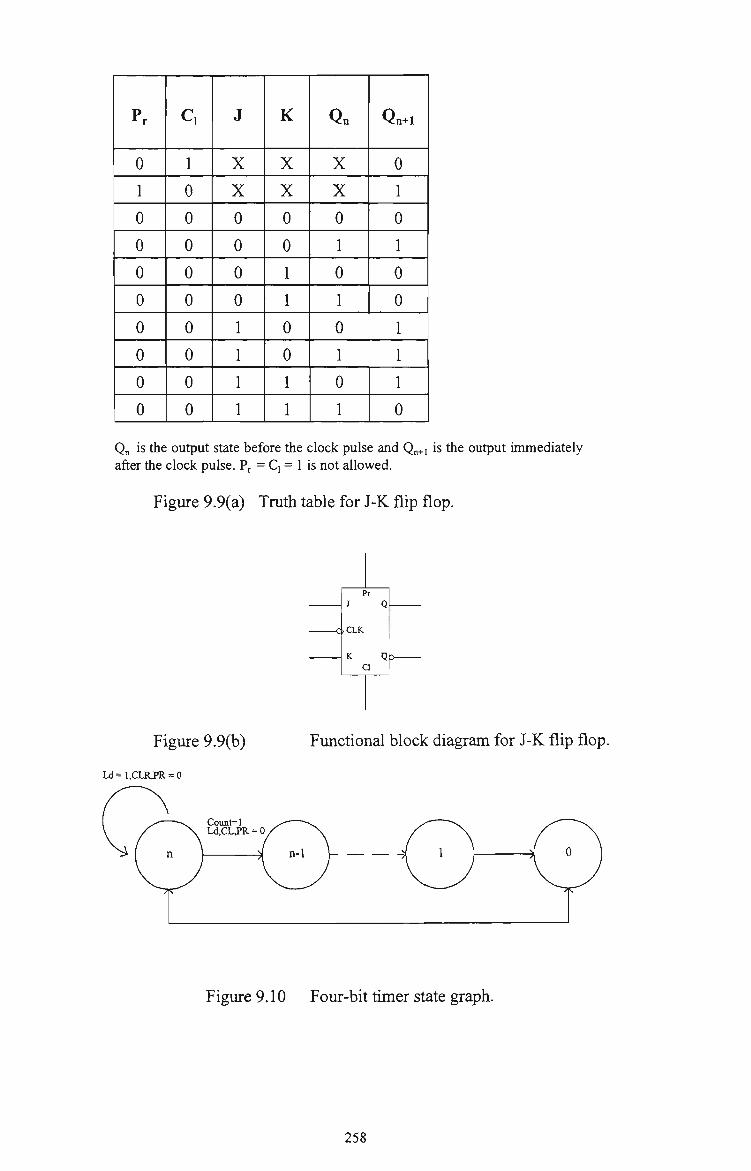
Pr
0
1
0
0
0
0
0
0
0
0
c,
1
0
0
0
0
0
0
0
0
0
J
X
X
0
0
0
0
1
1
1
1
K
X
X
0
0
1
1
0
0
1
1
Qn
X
X
0
1
0
1
0
1
0
1
Qn+1
0
1
0
1
0
0
1
1
1
0
Qn is the output state before the clock pulse and Qn+i is the output immediately after the clock pulse. P = Q = 1 is not allowed.
Figure 9.9(a) Tmtii table for J-K flip flop.
Pr J Q
<;>CLK
K QtD-Cl
Figure 9.9(b) Functional block diagram for J-K flip flop.
U=1,CLRJPR = 0
Figure 9.10 Four-bit timer state graph.
258

D C B A
0
0
0
0
0
0
0
0
1
1
1
1
0
0
0
0
1
1
1
1
0
0
0
0
1
1
0
0
1
1
0
0
1
1
0
0
1
1
0
0
1
0
1
0
1
0
1
0
1
0
1
0
1
0
1
0
D^ C^ B^ A^
0
0
0
0
0
0
0
0
1
1
1
1
0
0
0
0
1
1
1
1
0
0
0
0
1
1
0
0
1
1
0
0
1
1
0
0
1
1
0
0
1
0
1
0
1
0
1
0
1
0
1
0
1
0
1
0
1
JD
X
X
X
X
X
X
X
X
0
0
0
0
0
0
0
1
KD
0
0
0
0
0
0
0
1
X
X
X
X
X
X
X
X
Jc
X
X
X
X
0
0
0
1
X
X
X
X
0
0
0
1
Kc
0
0
0
1
X
X
X
X
0
0
0
1
X
X
X
X
JB
X
X
0
1
X
X
0
1
X
X
0
1
X
X
0
1
KB
0
1
X
X
0
1
X
X
0
1
X
X
0
1
X
X
JA
X
1
X
1
X
1
X
1
X
1
X
1
X
1
X
1
KA
1
X
1
X
1
X
1
X
1
X
1
X
1
X
1
X
DCBA and D C B A are the outputs ofthe timer immediately before and after the clock transition.
Figure 9.11 State table and input confrols for a four-bit timer.
The flip flop input equations in terms ofthe present state outputs for the four flip flops
are derived from the above state table and are described fry the following expressions:
JA=K, = \
J,=K, = A
Jc=Kc = B.A
J^=K^ = C.B.A
(9.4)
(9.5)
(9.6)
(9.7)
259

These expressions do not take into account the parallel load control. Parallel load is
realised via a two-to-one multiplexer at the inputs of each flip flop.
9.4.2.2 Structural Description
The J-K flip flop with asynchronous preset and clear fimctions has been realised using
NOR gates as shown ui Figure 9.12. This structure was chosen because it was readily
implementable in GaAs Technology. The outputs Q and Q remain unchanged during
the inactive interval of the clock. In addition the outputs remain unchanged during J =
K = 0, regardless ofthe clock transition. When the clock is active the flip flop operates
in a maimer as described by the truth table m Figure 9.9(a).
The four-bit timer has been realised using J-K flip flops, multiplexers with NOR gate
based confrol logic for the input. All the timer components were designed using E-D
GaAs Merged logic design technique. Figure 9.13 shows the logical implementation of
the one-bit timer cell.
CLK
Figure 9.12 Logic representation of J-K flip flop.
260

The operation ofthe four-bit timer is described as follows:
A. Normal time-out mode
Flip flop A is in toggle mode and toggles between logic level one and zero on the
falling edge ofthe clock pulse. The operation of flip flop depends upon the
output of flip flop A ortiy. Since A toggles at heilf the clock frequency, the output of flip
flop B toggles at fciock/4. Flip flop C depends upon the outputs of A and B, causing its
output to change at fdock/ - The operation of flip flop D depends upon the outputs of
flip flops A, B and C, causing its output to change at fdock/l . Thus the output
monitored from the four flip flops, DCBALSB» gives a pure binary count. Since the
input controls to each flip flop is from the complementary output of the previous stage,
the outputs follow a countdown sequence. Thus the circuit allows the time-out period
to be confrolled anywhere between l/fdock to 16/fciock-
B. Parallel load mode
Setting the multiplexer confrol input to logic zero, causes the timer operates in a normal
count down mode and for the multiplexer confrol mput set to one, the timer operates in
a parallel load mode. This enables the input data Pj to P4 to be loaded into the counter
on the falling edge ofthe next clock pulse, regardless ofthe logic levels present at the
other inputs. This fimction allows parallel loading ofthe counter.
C. Asynchronous controls
The preset and reset fimctions are asynchronous. A high level logic on reset input with
preset set to logic low level, sets all four of the flip flop outputs low regardless of the
261

logic levels present at the clock, load (multiplexer confrol input) or J K inputs.
Similarly setting the preset input to logic high level with reset set to logic zero level,
sets the outputs to logic high level, regardless of the logic levels present at the other
inputs.
9.4.2.3 Physical Description
The four-bit time-out timer cfrcuit was realised by butting single-bit timer cells with
interleaving NOR based control logic between each cell. The timer control inputs (load,
clock and asynchronous inputs) and parallel data inputs fed vertically into the cell with
J-K inputs and outputs propagating horizontally. This floor plan allowed easier butting
and reduced circuit height. The height of the timer remains constant with its width
mcreasing linearly as the bit size increases. Figure 9.14 shows a floor plan for a four-
bit timer.
Ld
P
ra
A
B
r
D
TJ\
Ld
P
E>n
Input Control Logic
^ .,
V^V
L^-^ ) \>
J ^ L ^
p
Clk 0
\ -^ ^ ^ j y° L
r>J ^ ; — ^ ) V)
I ^ r -
r J
>CLK
K C
c
r
r Q
J-K Flip lop Log
1
Figure 9.13 One-bit time-out tuner.
262

v Clear, clock and Databuses
.Gnd • Vdd
'A' Timer cell
withal! the logic
•B' D'
• Vdd .Gnd
I I I Figure 9.14 Four-bit timer floor plan.
Appendix J presents a detailed design procedure and performance for the timer.
9.4.3 VLSI Layout and Performance
The eight-bit comparator and the four-bit time-out timer were designed using GaAs
MESFETs with gate length of 0.8 micron. The circuits were designed using Merged
logic design technique. The layout methodology has sigruficant influence upon the
performance of the circuit. Commurtication paths between cells and positioning of
power and ground busses have significant influence upon the performance of high
speed VLSI systems. For example, fast transitions on signal bus could bring about
significant noise on the power bus. Thus, both the design methodology and layout will
have to address the influence of coupling between busses on performance.
The placement of power and ground busses adjacent to each other reduces their self
inductance, and hence their susceptibility to current transients. From the results of
coplanar strip line and coplanar waveguide models, placing of power buses in
263

proximity of each other reduces the inductance of the power bus by a factor of two or
more [106]. The ring notation approach, discussed in Chapter 5, exploits this advantage
and enables the designer to layout the skeleton of the cfrcuit rapidly, paying particular
attention to power and signal busses between adjacent cfrcuitry.
Using the above design methodology and layout approach, the eight-bit comparator and
the four-bit tuner cfrcuits were unplemented using ISD VLSI design suite. The VLSI
layouts for an eight-bit comparator and the four-bit timer cfrcuits are shown in Figures
9.15.
The above circuits have been analysed and evaluated using GaAs net exfractor and
HSPICE circuit simulation tools. The simulation results indicate a power dissipation of
18.48 nulliWatts for an eight-bit comparator with worst case propagation delay of
1.586 nanosec. The four-bit timer circuit dissipated 31.02 milliWatts of power with
propagation delays varying between 0.3232 nanosec to 0.4052 nanosec. The results for
an eight-bit comparator and the four-bit timer are tabulated in Table 9.1. The HSPICE
simulation waveforms for the cfrcuits are shown in Figure 9.16. Figure 9.16 (a) shows
the simulation results for an eight-bit comparator, where VINl, VIN2 and VIN3
represent bit A5, Cin (input to the most sigruficant stage) and cout (output of the list
sigruficant bit) respectively. The results indicate that when Cin is high, the inputs to the
lower bit stages have no effect on the output. With Cin set to logic '0', the output ofthe
comparator is determined by A and B mputs. The power waveform indicates the power
dissipated by the comparator cfrcuit. Figure 9.16 (b) shows the simulation results for
tiie four-bit tuner circuit, where VINl, VIN3, VIN4, VESfS and VIN6 represent the
264

clock pulse (phi), outputs A, B, C and D respectively. During tiie first 50 nanosecs, tiie
parallel load is enabled and tiie tuner is loaded witii tiie time-out value of DCBA =
1111. At 50 nanosecs the count is enabled and tiie tuner counts down to DCBA = 0000
witii tiie tune-out period of approximately 100 nanosecs. The power waveform
indicates the power dissipated by the four-bit timer cfrcufr.
m.13 SKBa S(tA2 GN;B2 GN:A1 GfCBl SKAO GKBO SKcotrt
Figure 9.15(a) Mask level layout of an eight-bh comparator.
SftC .6ftP4 sitcl EltO
Figure 9.15(b) Mask level layout of a four-bit timer.
V 0 L L I T N
V 0 L L I T N
500.OM
0.
500.OM
-1 1 I I I J L I. . 1. . I. . I. . L J I I 1 L L . L . I . I . I
SHS.OHSH V 0 L L I 500.OM r T N Z
— I . .1. .1. .1. .1. .1. .1. .1. .1. .1. .1. .1. .1. 0. 13.2^80M E-
. L . L . L . L . 1 . I . I . I . I . 1 .
WT flOL TTI 10.OM TflN
L p — ' • •'• •'• •<• •!• •'- i.-i- -I- -I. .1. .1. .1. .1. . 1 . L . L . 1 . 1 . 1 . L .c . 1 ., . 1 . I . I . , . , J :
10.ON 20.ON 30.ON 10.ON 50.ON °- TIME CLIN5 60.ON
- 8C0MP. - VINl - A
-• t '•
• • t 1 1 1 r t 1 1 1 1 1 r ) 1 1 1 1
-]i 1
. 1 . 1 . 1 . 1 — 1
SCOhP VIN2
- 8C0MP _: VIN3 - A
I . I . I . I . 1 . I _ i
—-f——J a 8C0MP
I POSER - A
Figure 9.16(a) Simulation waveforms for an eight-bfr comparator.
265

V L 0 I L N
5 0 0 . O M
0 .
^ '- 5 0 0 . O H r
L N fc—I
a s . s s s i M I I I I
V L 0 I L N,
500.OM r
9S .9310M u.
V L 0 I L N,
5 0 0 . O M
8 8 . t 6 0 1 M u
0 I s ^ o - ^ ^ r f 8 6 . 9 3 07M
KTL" flOI TTN
39 . 1192M
3 0 . OM
fUMMJ I I I 1 I
I I I i—t- I I
I I I I I r I I I I— I I
13 &-
t T I H E R V I N l
M T I M E R V I N 3
_ H T I H E R V I N H
, 1 ^
I T I M E R I ^ V I N 5
£, _ ' f T I M E R : V I N S
, , , a ^
nvTVtrtrp&rt^rrvHrnv^ IT IKER
ER
0. 50.ON I 00.ON
TIME CLIND
150 -ON 200 .ON 2C 0 . ON
Figure 9.16(b) Simulation waveforms for a four-bit timer.
9.5 VLSI Implementation of a Multi-Function
Multi-Protection Relay
An eight-bit multi-fimction multi-protection relay, containing an eight-bit comparator,
a four-bit time-out timer and a controller, was designed and implemented using
Integrated Silicon VLSI design suite. To obtain low power, high speed, good noise
margin and large fan out E-D GaAs Merged logic design techiuque was chosen. Figure
9.17 shows the floor plan for the multi-fimction multi-protection relay. It encompasses
all the necessary design criteria, including placement of the input and output signals so
that the cells can be assembled with mirumum length routing paths between cells.
Figure 9.18 shows the VLSI layouts ofthe a eight-bit multi-fimction multi-protection
relay.
266

8-btt Comparator Jv ? Controller
y^K Power ground busses
4-bit Timer
Figure 9.17 Floor plan for an eight-bit multi-fimction multi-protection relay.
Figure 9.18 VLSI layout of an eight-bit multi-fimction multi-protection relay.
9.6 Simulation and Performance
An eight-bit multi-function multi-protection relay was anedysed and evaluated usmg
GaAs net extractor and HSPICE cfrcuit simulation tools. The results are summarised in
Table 9.2. Figure 9.19 shows the HSPICE simulation results, for an eight-bit multi-
fimction multi-protection relay, where VIN3, VIN4, VIN5, VIN6, VIN7 and VIN8
represent relay output, comparator output, and the A, B, C, D outputs ofthe timer. The
result shows that the relay loads the time-out number in the timer and waits for the
confroller to signal start of time-out period. This happens at 50 nanosecs, and the timer
starts the time-out period. At the end of this period, with the confroller
267

Table 9.1 Simulation results for an eight-bit comparator and the four-bit
timer
Description
Number of devices
E-MESFET
D-MESFET
Gate Length
Propagation Delay
Cg to Co
O toA
O toB
O toC
O toD
Rise Time
Co
A
B
C
D
Fall Time
Co
A
B
C
D
Power Dissipation
Noise Margin
Eight-bit Comparator
144
80
64
0.8 micron
1.586 nanosec
0.2473 nanosec
0.2215 nanosec
18.48 milliwatts
0.30 Volts
Four-bit timer
231
145
86
0.8 micron
0.4052 nanosec
0.3702 nanosec
0.3283 nanosec
0.3232 nanosec
0.9495 nanosec
0.3210 nanosec
0.2134 nanosec
0.2039 nanosec
1.136 nanosec
0.6844 nanosec
0.3701 nanosec
0.3645 nanosec
31.02
milliWatts
0.30 Volts
indicating the input value still greater than the set value, an output pulse is generated, as
indicated by VIN3. At 300 nanosecs the controller signals the input value less than the
set value, resets the timer and waits for the signal from the comparator to start the
268

time-out period. From the results it can also be seen that this design technique gives
large logic swings resulting in excellent noise margins. The chip dissipates 49.73
nulHWatts of power, indicating the suitability of this design technique in implementing
VLSI cfrcuits.
V L 5 0 . O M I T " "
0 I
^ ^ 0 .
P I I I I I I i'» I'l > I i - v ^ i I 1 t I !• »-l'i I' • I i!i ' I J •' !• ' - t I I >'-*• I I I ) I I I I r 1 ^ pp. „ „
Z PO«ER j . . . . . . . , J i ^ .L. J . . . 1 . . . J . . . 1 . . 1 . . . 1 . . . 1 . . . I
V L I 0 1 5O0 .OM I " I ll L N
0 . I, > I...', i , - : . j m i : .t.l.i )J. U .J . l i l . l iiti.i.l.L....i.
V L 5 D 0 . OM r 0 I L N
.^ R E L f l t = VINM
V L 5 0 0 . O M r -
0 I §j L N
r~iAiwiiiipftfwiir^B . 1 . . . 1 . . . L . . . 1 . . . r . . J . . . 1 . . . J . . . 1 . . . T . . . 1 . . . I . . . 1 . . . I . . . 1 . . . I. •. 1—1
AT 5
0. — . I . . .1. . . L . . .1. J . . .1. . . J . . .1. .1, .. I . . . ) . . . t
- R E L A Y - V I N S -, ^
V L 500.0M jT-0 1 . I
. 1 . . J . . . I . . .1 . . J . . .1. . . J . . .1. .1. . . I . . .1. . . t ff
. I . . .1
— R E L R T - V I N 7
£1
^ >- 5 0 0 . O M 0 I
^ - 0. I • : — RELflT
1 I VIN8 I . . .1. . . 1. . . .1. . .1. . . J . . .1. . . J. . .1. . . I . . .1. . . 1 - . .1. . . I • • .1. . - 1 • • J - J
100 . ON 200 . ON 3 0 0 .ON 0. TIME C L I N ) 3 5 0 . ON
Figure 9.19 Simulation waveforms of the relay. VIN3 represents the trigger pulse generated after each time out period of 150 ns and 265 ns.
Table 9.2 Performance of an eight-bit multi-function multi-protection relay
Description
Number of devices
E-MESFET
D-MESFET
Gate length
Power dissipation
Noise margin
Eight-bit relay
400
240
160
0.8 micron
49.73 miUiWatts
0.30 Volts
269

9.7 Conclusions
The design and unplementation of an eight-bfr multi-fimction, multi-protection relay
chip for power systems protection has been presented in this chapter. E-GaAs
fabrication technology was chosen as a senuconductor medium because of its high
electron mobility and existence of semi-insulating substrate properties. Merged logic
design approach was used to design all the components of the relay. This approach to
circuit design combines direct coupled MESFET logic (DCFL) with source follower
DCFL (SDCFL) and source follower MESFET logic (SFFL) so tiiat tiie advantages of
each logic class are exploited and circuit performance is achieved which is superior to
that obtained from different design approaches. In this technique, DCFL is
predominantly used to achieve higher packing density and improved cfrcuit
performance. SDCFL design techiuque is used to drive large capacitive loads and
realise the And-Or-Invert fimctions while SFFL design technique is used to implement
large fan out.
The eight-bit relay chip was designed and implemented with 400 E-D GaAs MESFETs
and dissipated 49.73 milliWatts of power. Results indicate a very high speed operation
ofthe relay with respectable noise margin. The performance indicated the validation of
the GaAs technology and Merged logic design techruque to very fast integrated circuit
design for power systems protection.
270

Chapter Ten
Conclusions
The reward ofa thing well done is to have done it.
Proverb.
10.0 A Retrospective Overview of this Thesis
In this thesis, research has been conducted on the analysis of GaAs design techniques,
the development of new static and dynamic design techniques in GaAs technology and
design, implementation and performance analysis of a four-bit multi-channel data
acquisition and an eight-bit multi-function multi-protection relay chips. The following
stages of research are essential in the development of new GaAs MESFET design
techniques to be used in the implementation ofthe above chips.
(i) Review of the VLSI cfrcuit design technologies available and to
determine the most suitable technology in the design of very high speed
and low power integrated cfrcuits.
271

(ii) Modelling the devices to be used in the given technology,
(iii) Having decided on the VLSI fabrication technology, review, design,
analysis and evaluation of the currently available VLSI cfrcuit design
techniques and assessment on the suitability of these techniques for high
speed low power VLSI cfrcuit implementation,
(iv) Development, design, analysis and evaluation of design techniques for
the implementation of high speed low power integrated circuits.
Technology review in Chapter 2 highlights that for very high speed operation in a
semiconductor medium, three factors become significant, namely, carrier mobility,
carrier saturation velocity, and existence of semi-insulating substrate. GaAs technology
mostiy fiilfils the requfrements, and together with low power dissipation provide a
technology base for fiiture VLSI cfrcuits design.
Analysis ofthe currently available VLSI design techniques in GaAs technology reveals
that though the normally-on static logic design techniques offer very high speed
operation, they suffer from high power dissipation. Since the normally-on cfrcuits are
based on D-MESFETs, usually two power supplies are requfred for proper operation of
these circuits. These make normally-on logic circuits unattractive for VLSI cfrcuits
design.
272

Normally-off static logic, on the other hand uses E-MESFETs for switching and also
requfres only single power supply. Although these techniques are being extensively
used for VLSI circuit design, they suffer from a number of lintitations such as low
noise margins, sensitivity ofthe gate delay to fan in and fan out and load capacitance.
TDFL dynamic circuit design techniques offered much smaller chip size per function
resulting in much lower power dissipation but sufifers from poor drive capability.
Domino dynamic technique, on the otiier hand, has a very good drive capability.
One ofthe major problems in realising cfrcuits in GaAs MESFET technology is caused
by the dispersion ofthe device characteristics throughout the chip and wafer. The SCFL
circuit design technique is such that ortiy the relative variations of the threshold voltage
is important. The evaluation of the design technique shows that SCFL cfrcuit design
techiuque is the best choice in the GaAs MESFET process for a mixed of digital and
analog integrated cfrcuits implementation on the same chip.
Two design techruques using GaAs MESFET technology have been developed to
overcome some of the limitations of the normally-off static logic and the dynamic
domino cfrcuit design techniques. Merged logic design technique is developed using
normally-off static logic and Multiple-output dynamic domino technique has been
developed for dynamic circuits.
The Merged logic technique to circuit design combines direct coupled MESFET logic
(DCFL) witii source follower DCFL (SDCFL) and source fotiower MESFET logic
(SFFL) so that the advantages of each logic class are exploited and cfrcuit performance
273

is achieved which is superior to that obtained from different design approaches. In the
Merged logic static design technique, DCFL is predominantly used to achieve higher
packing density and improved circuit performance. SDCFL technique is used to drive
large capacitive loads and realise the And-Or-Invert fimctions while SFFL is used to
implement large fan out. This technique involves identifying critical parts ofthe cfrcuit
where SDCFL and SFFL techniques can be used to improve cfrcuit performance.
The performance of Merged logic design approach is illustrated witii tiie design,
implementation and performance analysis of a power series evaluator chip. From the
performance analysis it can be seen that this design approach demonsfrates excellent
circuit performance.
The principle behind multiple-output domino technique is the utilisation of the sub-
fimctions available in the logic tree ofthe domino gates. Multiple outputs are available
by adding precharge devices at the corresponding intermediate nodes in the logic tree.
Since the saving in the area is mairtiy due to a reduction of replication of sub-circuits,
the actual advantage of this design technique over domino logic design technique is
directly dependent upon the number of recurrence in a logic function being realised.
The performance advantage of this design techruque over dynamic domino technique
has been demonsfrated via the implementation ofa four-bit CLG for a Carry Lookahead
Adder. The multiple-output domino technique demonsfrates increased cfrcuit
performance, reduced circuit area and power dissipation when compared with the
domino technique. This is due to the reduction in the parasitic capacitance and output
274

loading. The most remarkable achievement using this techruque is the reduction in the
number of devices requfred to implement the CLG cfrcuit. The performance of
multiple-output domino is fiirther improved by graded scaling ofthe domino chain.
Design, implementation and analysis of two VLSI chips are presented using the GaAs
MESFET design techniques developed. Ulfra fast four-bit multi-charmel data
acquisition chip was designed and implemented in E-D GaAs MESFET technology
using 0.8 micron gate lengths. Appropriate design techruques and technology have been
chosen for the design of this ntixed analog-digital chip. SCFL technique was chosen in
the design of a mix of digital and analog circuits on the same chip, mainly because of
its wide tolerance to threshold voltage range and its immunity to temperature
variations. It also has an excellent fan out capability, a small input capacitance and a
small discharging time permitting high speed operations. Digital components were
designed using GaAs Merged logic design technique.
Design of a flash ADC requfres ortiy 2 ° ' ^ comparators to implement a n-bit flash
ADC as compared with (2" - 1) comparators required for a classical n-bit flash ADC.
This greatiy reduces the complexity ofthe flash ADC. Depending upon the application,
high resolution ADC can easily be cascaded using four-bit flash ADC modules.
The four-bit multi-charmel data acquisition chip is implemented with 397 devices and
dissipates 185.6 milliWatts of power. The conversion time is 0.85 nanosec with noise
margm of 0.35 Volts. These results indicate the appropriateness of the design
technology and techniques used for mixed analog-digital cfrcuit design on a single chip.
275

An eight-bit multi-function multi-protection relay chip for power systems protection
has been designed and implemented in GaAs technology usuig Merged logic cfrcuit
design technique. The relay chip is developed using eight-bit comparator, fully
programmable four-bit time-out timer and a controller with necessary handshake logic.
The eight-bit magrutude comparator urut compares the incoming signals (phase and
line currents and voltages) with the set (normal) values of these signals, stored as look
up table in a memory, and generates a control signal if the magrutude of the incoming
signal is greater than the set value. The time-out periods ofthe timer are stored as look
up table in a Read Ortiy Memory based on defirute and inverse time-current
characteristics of the relay. This is dowrtioaded into the timer using parallel load
facilities. The controller unit morutors the comparator output and send a signal to timer
unit to either start time-out period or load the time-out value. At the end of time-out
period if the magrutude of the incoming signal is still greater than the set value, a
frigger pulse is generated by the confroller unit to operate appropriate cfrcuit breakers.
It also provides handshake signals for other relays in the synchronous protection
scheme. This structure gives the flexibility for the relay to be used as multi-function,
multi-protection device. A cellular design approach has been used to give the flexibility
to tiie system to be easily cascaded into multi-bfr (sixteen, thirty two, etc) multi
function multi-protection relay.
The eight-bit relay chip is implemented with 400 GaAs MESFETs and dissipates 49.73
miUiWatts. The performance indicate the validation of the GaAs technology and
276

Merged logic design technique for the implementation of high speed low power
mtegrated cfrcuits.
The primary objective in the layout of GaAs cfrcuits is optimum exploitation of the
performance offered by the GaAs technology. This can be achieved only when the
layout guarantees minintisation of parasitic capacitances. Full custom design approach
has been used for all the design layout with the entfre operation implemented on a
single chip rather than on multiple chips. This allows to maxunise on the advantages of
the GaAs technology and reduce parasitic capacitances due to chip intercormections.
In conclusion, all the aims of this research have been successfully met.
10.1 Avenues to be Explored in Further Work
The only limits of our realisation of tomorrow will be our doubts of today.
Franklin D. Roosevelt
The studies reported in this thesis involve the development of new design techniques in
GaAs technology using both static and dynamic approaches and design,
unplementation, simulation and analysis of a four-bit multi-charmel data acquisition
chip and an eight-bit multi-fimction multi-protection chip. The following aspects
relating to the future research into VLSI cfrcuits and systems design are suggested:
277

(i) Design and implementation of VLSI cfrcuits using high elecfron
mobility fransistors (HEMTs) instead of MESFETs. Since HEMT
devices belong to the E-MESFET family of technologies, they enjoy the
inherent advantages and disadvantages of such technologies. For
example, the variance of threshold voltage of about 10 rrtillivolts must
be obtained in HEMT VLSI cfrcuits. The improvements in GaAs
fabrication technologies and superior control offered by MBE is
inherently capable of attairung this degree of uniformity. An important
advantage of HEMT devices is that they achieve their high speed at
lower logic voltage swings than E-MESFETs, which may result in
dynamic power dissipation of one to two orders of magrutude lower.
Although the small logic swing may compromise the cfrcuit noise
margin, low power is of great importance in VLSI circuit applications.
(u) Design and implementation of VLSI circuits using hetrojunction bipolar
transistors (HBTs). Performance of HBT devices ultimately projected to
be in the 100 - 200 GHz range with gate delays m the range of 10
picosec. Furthermore, the high current drive capability of HBTs coupled
with their threshold voltage insensitivities makes these devices the prime
candidate for ultra high performance VLSI integrated circuits.
(iii) The multi-function multi-protection relay can be fiirther improved by
incorporation of multi-channel data acquisition and the memory circuits
on the same chip. This will result in lower chip interconnection
278

capacitance leading to higher speed, lower power dissipation and giving
greater application flexibility.
(iv) Integration of sensors and signal conditioning cfrcuits on multi-channel
data acquisition chip will enable it to be used as micro-machine with
digital signal available at the outputs. This will find major applications
in remote sensoring.
279

Bibliography
[1] Suyama, K., Kusakawa, H., Okamura, S. and Fukuta, M., "An MSI GaAs
integrated circuit: 4-bfr arithmetic and logic unit", IEEE Joumal on Solid-State
Circuits, Vol. SC-17, No. 4, pp 653 - 657, 1982.
[2] Deming, R.N., Zucca, R., Vahrenkamp, R.P., Hou, L.D., Naused, B.A. and
Gilbert, B.K., "A gallium arserude configurable cell array using buffered fet
logic", IEEE Joumal of Solid-State Cfrcuits, Vol. SC-19, No. 5, pp 728 - 738,
1984.
[3] Rocchi, M. and Gabillard, B., " GaAs digital dynamic ICs for applications up
to 10 GHz", IEEE Joumal of Solid-State Circuits, Vol. SC-18, No. 3, pp 369 -
376, 1984.
[4] Hirayama, M., Ino, M., Matsuoka, Y. and Suzuki, M., "A GaAs 4 kbit SRAM
witii direct coupled fet logic", IEEE Joumal of Solid-State Cfrcuits, Vol. SC-19,
No. 5, pp 716-720, 1984.
[5] Osafune, K., Enoke, T., Yamasaki, K. and Ohwada, K., "GaAs ultra high
frequency dividers with advanced SAINT fet's", IEEE Trans, on Electron
Devices, Vol. ED-33, No. 12, pp 2059 - 2063, 1986.
280

[6] Suigh, H.P., Sadler, R.A., Irvine, J.A. and Gorder, G.E., "GaAs low power
integrated circuits for high speed digital signal processing", IEEE Trans, on
Electron Devices, Vol. ED-36, No. 2, pp 240 - 249, 1989.
[7] Katsu, S., Nambu, S., Shunano, A. and Kano, G., " A GaAs monolithic
frequency divider using source coupled fet logic", IEEE Electron Device Letter,
Vol. EDL-3, No. 8, pp 197 -199, 1982.
[8] Katsu, S., Nambu, S., Shimano, A. and Kano, G., "A source coupled fet logic -
a new current mode approach to GaAs logics", IEEE Trans, on Electron
Devices, Vol. ED-32, No. 6, pp 1114 - 1118,1985.
[9] Idda, M., Takada, T. and Sudo, T., " Analysis of high speed GaAs source
coupled fet logic circuits", IEEE Trans, on Microwave Theory and Techniques,
Vol. MTT-32, No. 1, pp 5 - 10, 1984.
[10] Vu, T.T., Peczalski, A., Lee, K.W. and Conger, J., "The performance of source
coupled fet logic circuits that use GaAs MESFET's", IEEE Joumal of Solid-
State Circuits, Vol. SC-23, No. 1, pp 267 - 279, 1988.
[11] Ohta, N. and Takada, T., "High speed GaAs SCFL monolithic integrated
decision circuit for Gbit/s optical repeaters", Electrorucs Letter, Vol. 19, No.
23, pp 983-985, 1983.
281

[12] Shinuzu, S. et al., "A 1 Ghz 50 mW GaAs dual modulars divider using source
coupled fet logic", ISSCC Digest Technical Papers, pp 52 - 53, 1984.
[13] Vu, T.T. et al, "A gallium arsenide SDFL gate array with on-chip RAM", IEEE
Joumal of Solid-state Circuits, Vol. SC-19, No. 1, pp 10 - 22, 1984.
[14] Vu, T.T. et al., "Low power 2K cell SDFL gate array and DCFL circuits using
GaAs self-aligned E/D MESFET's ", IEEE Joumal of Solid-State Cfrcuits, Vol.
SC-23, No. 1, pp 224 - 236, 1988.
[15] Shur, M.S. et al., "Design and simulation of self-aligned modulation doped Al
GaAs/GaAs ICs", ISSCC Digest Techrucal Papers, pp 264 - 265,1985.
[16] Srivastava, A. and Dubey, M., "GaAs digital integrated cfrcuits - a review from
silicon point of view for desigiung ultra fast VLSI circuits", IEEE Joumal of
solid-state Cfrcuits, Vol. 25, pp 1250 -1254, 1990.
[17] Higashiska, N. et al., "GaAs DCFL 2.5 Gbps 16-bfr multiplexer/demultiplexer
LSI's", IEEE Joumal of Solid-State Circuits, Vol. SC-29, No. 7, pp 808 - 814,
1994.
[18] Singh, H.P., Sadler, R.A., Tanis, W.J. and Schenberg, A.N., "GaAs prescalers
and counters for fast settlmg frequency synthesisers", IEEE Joumal of Solid-
State Circuits, Vol. SC-25, No. 1, pp 239 - 245, 1990.
282

[19] Singh, H.P., Sadler, R.A., Geissberger, A.E. and Tanis, W.J., " High speed low
power GaAs programmable counters for synthesiser applications", IEEE GaAs
IC Symposium Technical Digest, pp 269 - 272, 1987.
[20] Pasternak, J.H. and Salama, C.A.T., "GaAs MESFET differential pass transistor
logic", IEEE Joumal of Solid-State Cfrcuits, Vol. SC-26, pp 1309 - 1316, 1991.
[21] Hoe, D.H.K. and Salama, C.A.T., " GaAs trickle tt-ansistor dynamic logic",
IEEE Joumal of Solid-State Circuits, Vol. SC-26, pp 1441 -1448, 1991.
[22] Yang, L., Chakhararapani, R. and Long, S.I., "A high speed dynamic domino
circuit implemented with GaAs MESFET's", IEEE Joumal of Solid-State
Circuits, Vol. SC-22, No. 5, pp 874 - 879,1987.
[23] Nary, K.R. and Long, S.I., "Dynamic latch for high speed GELAS domino
circuits", Elecfronics Letter, Vol. 28, No. 1, pp 36 - 37, 1992.
[24] Krambeck, R.H., Lee, C.H. and Law, H.S., "High speed compact cfrcuits with
CMOS", IEEE Joumal of Solid-State Circuits, Vol. SC-17, No. 3, pp 614 - 619,
1982.
[25] Lassen, P.S., Long, S.I. and Nary, K.R., "Ulfra low power GaAs MESFET MSI
circuits using two phase dynamic fet logic", IEEE Joumal of Solid-State
Circuits, Vol. SC-28, No. 10, pp 1038 - 1045, 1993.
283

[26] Nary, K.R. and Long, S.L, " GaAs two phase dynamic fet logic: a low power
logic family for VLSI", IEEE Joumal of Solid-State Cfrcuits, Vol. SC-27, No.
10, pp 1364-1371,1992.
[27] Corcoran, J., Poulton, K. and Homak, T., "A 1 Ghz 6b adc system", ISSCC
Digest Technical Paper, pp 102 - 103, 1987.
[28] Thomas, F. et al., "1 Ghz GaAs adc building blocks", IEEE Joumal of Solid-
State Circuits, Vol. SC-24, No. 2, pp 223 - 228,1989.
[29] Ducourant, T. et al., "3 Ghz, 150 mW, 4 bit GaAs analog to digital converter",
IEEE GaAs Symposium, pp 209 - 212, 1986.
[30] Ducourant, T., Meignant, D., Bertsch, P. and Wright, M., "A 5 bit, 2.2 Gs/s
monolithic analog to digital converter with gigahertz bandwidth, and 6 bit a/d
converter system", IEEE GaAs Symposium, pp 337 - 340,1989.
[31] Naber, J.F., Singh, H.P., Sadler, R.A. and Milan, J.M., " A low power high
speed 4-bit GaAs adc and 5-bit dac", IEEE GaAs Symposium, pp 333 - 336,
1989.
[32] Kleks, J. et al., "A 4-bit single chip analog to digital converter with 1.0
gigahertz analog input bandwidth", IEEE GaAs Symposium, pp 79 - 82, 1987.
284

[33] Hagelauer, R. et al., "A gigasample/s 5 bit adc with on-chip track & hold based
on an industrial 1 |im GaAs MESFET E/D process", IEEE GaAs S5miposiiim,
pp 365-368, 1991.
[34] Sauerer, J. et al., "System architecture and key components for an 8 bit/1 GHz
GaAs MESFET adc", IEEE GaAs Symposium, pp 105 -108, 1992.
[35] Doemberg, J. and Hodges, D.A., "A 10-bit 5 megasamples/sec CMOS 2-step
flash adc". Proceeding of IEEE Custom Integrated Circuits Conference, pp
18.6.1 -18.6.4, 1988.
[36] Kerth, D.A., Sooch, N.S. and Swanson, E.J., "A 667 ns, 12 bit, two step flash
adc", Proceeding of IEEE Custom Integrated Circuits Conference, pp 18.5.1 -
18.5.3, 1988.
[37] Hagelauer, R. et al., "Investigations and measurements of the dynamic
performance of high-speed adc's", IEEE Trans, on Instrumentations and
Measurement, Vol. 41, No. 6, pp 829 - 833, 1992.
[38] Balsubramanian, K., "A flash adc with reduced complexity", IEEE Trans, on
Indusfrial Electt-onics, Vol. 42, No. 1, pp 106 -108,1995.
[39] Sachdev, M.S., "Microprocessor relays and protection systems", IEEE tutorial
course text, PubhcationNo. 88EH0269-1-PWR, 1988.
285

[40] Kramer, CA. and Elmore, W.A., "Flexible inverse overcurrent relaying using a
microprocessor", IEEE Trans, on Power Delivery, Vol. 5, No. 2, pp 915 - 921,
1990.
[41] Sidhu, T.S., Wood, H.C. and Nagpal, M., "Design, implementation and testing
of a microprocessor based high speed relay for detecting transformer winding
faults", IEEE Trans, on Power Delivery, Vol. 7, No. 1, pp 108 - 117, 1992.
[42] Manzol, M.A., "Multiple overcurrent relays using a single microprocessor",
IEEE Trans, on Industrial Electronics, Vol. 37, No. 4, pp 307 - 309,1990.
[43] Harlow, J.H., "Applying a multifunction protection relay for the cogeneration
industry", Beckwith Electric Company, Inc Largo, Florida. Topical Report, pp
153-158,1991.
[44] Gillany, M.T., Makil, O.P. and Hope, G.S., "A digital protection technique for
parallel fransmission lines", IEEE Trans, on Power Delivery, Vol. 7, No. 1, pp
118-125,1991.
[45] Yalla, V.V.S., "A digital multifunction protective relay", IEEE Trans, on Power
Delivery, Vol. 7, No. 1, pp 193 - 201, 1992.
286

[46] Balasubramanian, K. and Oral, M., "Microprocessor based multi-function relay
switching", IEEE Trans, on Consumer Electronics, Vol. 38, No. 4, pp 878 - 883,
1983.
[47] Zayegh, A., Kalam, A. and Chen, J., "32-bh microprocessor based digital
relaying techniques for overcurrent and differential protection", Proc. of Int.
AMSE Conf, AMSE Press, Vol. 3, pp 81 - 87, 1992.
[48] Woerlee, P.H. et al, "A low power 0.25 |im CMOS technology", IEEE
Intemational Electron Devices Meeting, pp 31 - 34, 1992.
[49] Lee, Y.J., Garvin, H.L. and Slayman, C.W., "A high-speed high-density sihcon
8 X 8-bit parallel multiplier", IEEE Joumal on Solid-State Cfrcuits, Vol. SC-22,
pp 35-40, 1987.
[50] Hunt, P.C. and Cooke, M.P., "Process HE: a highly advanced trench isolated
bipolar technology for analogue and digital applications'', Proceeding IEEE
Custom Integrated Circuits Conference, 22.2.1_- 22.2.4, 1988.
[51 ] Washio, K., Nakazato, K. and Nakamura, T., "2.7 ns 8 x 8-bfr parallel multiplier
using side wall base contact structure", IEEE Joumal on Sotid-State Cfrcuits,
Vol. SC-22, pp 613 - 614,1987.
287

[52] Nakayama, Y. et al., "A GaAs 16 x 16-bit parallel multiplier", IEEE Joumal on
Solid-State Circuits, Vol. SC-18, pp 599 - 603, 1984.
[53] Goel, A.K. and Kalia, A., "Comparison of NMOS, CMOS and GaAs
technologies". Proceeding of IEEE Midwest Symposium on Cfrcuits and
Systems, pp 1238 -1241, 1990.
[54] Brunvand, E., Michel, N. and Smith, K., "A comparison of self-timed design
using FPGA, CMOS ans GaAs technologies", IEEE Intemational Conference
on Computer Design: VLSI in Computers and Processors, pp 76 - 80, 1992.
[55] Elrabaa, M. and Elmasry, M.I., " Multi-emitter BiCMOS cml circuits", IEEE
Joumal on Solid-State Circuits, Vol SC-24, pp 454 - 458, 1992.
[56] Chen, C.L., "Level shifted and voltage reduced 0.5 fim BiCMOS circuits",
IEEE Intemational Solid-States Conference, pp 236 - 237, 1990.
[57] Rofail, S.S, "low voltage, low power BiCMOS digital circuits", IEEE Joumal of
SoHd-States Cfrcuits, Vol. 29, No. 5, pp 572 - 579, 1994.
[58] Bellaaouar, A. and Touzene, H., "3.3 V BiCMOS current-mode logic circuits
for high speed adders", IEEE Joumal of Solid-States Circuits, Vol. 31, No. 8, pp
1165-1169,1996.
288

[59] Kuraha, S. et al., "A 6 ns 1.5 V 4 Mb BiCMOS SRAM", IEEE Intemational
SoUd-States Conference, pp 144 -145, 1996.
[60] Murabayashi, F. et al, "3.3V BiCMOS cfrcufr techniques for a 120 Mhz RISC
microprocessor", IEEE Joumal of Solid-States Cfrcuits, Vol. 29, No. 3, pp 298 -
302,1994.
[61] Liu, T.M. et al., "A half-micron super self-aligned BiCMOS technology for
high speed applications", IEEE Intemational Electron Devices Meeting, pp 23 -
26,1992.
[62] Suzuki, M. et al., "A 3.5-ns, 500-mW, 16-bfr BiCMOS ECL RAM", IEEE
Joumal of Solid-States Circuits, Vol. 24, No. 5, pp 1233 - 1237, 1989.
[63] Wanlass, F.M. and Sah, C.T., "Nanowatt logic using field effect MOS triodes",
IEEE Solid-States Conference Technical Digest, pp 32 - 35, 1963.
[64] Mukherjee, A., "Infroduction to nMOS and CMOS VLSI systems design",
Prentice Hall, 1986.
[65] Ning, T.H. and Tang, D.D., "Bipolar trends", IEEE Joumal on Solid-State
Circuits, Vol. SC-74, No. 12, pp 1669 -1677, 1986.
289

[66] Kapoor, A.K. and Roulston, D.J., "Polystiicon emitter bipolar transistors", IEEE
Press, 1989.
[67] Kobayashi, T., Nakayama, S., Miyake, M. and Okazaki, Y., "Nitrogen in-situ
doped poly buffer LOCOs: simple and scalable isolation technology for deep-
submicron silicon devices", IEEE Intemational Electron Devices Meeting, pp
683 - 686, 1994.
[68] Ohzone, T., Iwata, H., Uraoka, Y. and Odanaka, S., "Two dunensional analysis
of holt-carrier photoemission from LOCO- and trench-isolated MOSFETs",
IEEE Intemational Elecfron Devices Meeting, pp 527 - 530, 1992.
[69] Embabi, S.H.K., Bellaouar, A. and Ehnasry, M.I., "Digital BiCMOS integrated
circuit design", Kluwer Academic Publication, 1993.
[70] Yamaguchi, T. and Yuzuriha, T.H., "Process integration and device
performance of a submicron BiCMOS with 16-GHZ f^ double poly-biploar
devices", IEEE Trans, on Electt-on Devices, Vol. 36, No. 5, pp 890 - 896, 1989.
[71] Kua, J.B., Su, K.W. and Lou, J.H., "1.5V BiCMOS dynantic multiplier using
Wallace tree reduction architecture", lEE Electronics Letter, Vol. 29, No. 24, pp
2097 - 2098,1993.
290

[72] Robertson, D.H., "BiCMOS techniques for high speed, high resolution adcs",
IEEE Intemational Symposium on Cfrcuits and Systems, Vol. 6, pp 2695 -
2698,1992.
[73] Chang, Y.C. and Francis, K., "GaAs high-speed devices", John Wiley and Sons,
Inc., 1994.
[74] Pucknell, D.A. and Eshraghian, K., "Basic VLSI design", Third Edition,
Prentice Hall, 1994.
[75] Kanopoulos, N., "Gallium arserude integrated circuits". Prentice Hall, 1989.
[76] Shah, D.M. et al, "Epitaxial lift-off GaAs HEMT's", IEEE Trans, on Electron
Devices, Vol. 42, No. 11, pp 1877 -1881, 1995.
[77] Yang, Y.F., Hsu, C.C. and Yang, E.S., "Integration of GalnP/GaAs
hefrojunction bipolar transistors and high elecfron mobility transistors", IEEE
Electron Devices Letter, Vol. 17, No. 7, pp 363 - 365, 1996.
[78] Canfield, P.C. and Allostat, D.J., "A potential for p-well GaAs technology for
precision mtegrated circuits", IEEE Symposium on Cfrcuits and Systems, pp
3065 - 3068, 1990.
291

[79] Shur, M.S., "Analytical model of GaAs fet's", IEEE Trans, on Electron
Devices, Vol. ED-32, pp 70 - 72, 1985.
[80] Tuyl, R.V. and Liechti, C.A., "Gallium arsenide digital integrated cfrcuits",
Airforce Aviorucs Laboratory, AFSC, WPAFB, Teclmical Report AFAL-TR-74
-40,1974.
[81] Pucel, R., Haus, H. and Statz, H., "Signal and noise properties of gallium
arserude microwave field-effect transistors". Academic Press, pp 195 - 205,
1975.
[82] Krumm, C.F. et al., "Low noise field effect transistors", Huges Research Labs.,
AFAL-TR-78-182, 1978.
[83] Curtice, W.R., "A MESFET model for use m tiie design of GaAs integrated
circuits', IEEE Trans, on Microwave Theory and Techruques, Vol. MTT-28,
No. 5, pp 448-455, 1980.
[84] McCamant, A.J., McCormack, CD. and Smith, D.H., "An improved GaAs
MESFET model for SPICE", IEEE Trans, on Microwave Theory and
Techniques, Vol. MTT-38, pp 822 - 824, 1990.
[85] Sakurai, T. ans Newton, A.N., "A sunple MOSFET model for cfrcuit analysis",
IEEE Trans, on Elecfron Devices, Vol. 38, pp 887 - 893,1991.
292

[86] De, V.K. and Meuidl, J.D., " Three-region analytical models for MESFET's m
low-voltage digital circuits", IEEE Joumal of Solid-State Circuits, Vol. SC-26,
No. 6, pp 850 - 857, 1991.
[87] De, V.K. and Meindl, J.D., "An analytical tiireshold voltage and subthreshold
current model for short-channel MESFET's", IEEE Joumal of Solid-State
Circuits, Vol. SC-28, No. 2, pp 169 -172,1993.
[88] Chang, C.T.M. et al., "A subthreshold current model for GaAs Mesfet's", IEEE
Electron Devices Letters, Vol. 8, No. 2, pp 69 - 72, 1987.
[89] Conger, J., Peczalski, A. and Shur, M.S., "Subthreshold current in GaAs
MESFET's", IEEE Electron Devices Letters, Vol. 9, No. 3, pp 128 - 129, 1988.
[90] Helix, M.J. et £d., "Improved logic gate with a push-pull output for GaAs digital
ICs", Proceeding of Intemational GaAs Symposium, pp 108 - 111, 1982.
[91] Beaumont-Smith, A. and Eshraghian, K., "Comparison of Gallium Arserude
MESFET process technologies". Technical Report GaAs 92-14, 1992.
[92] Lehovec, K. and Zuleeg, R., "Analysis of GaAs fet's for integrated logic", IEEE
Trans, on Electt-on Devices, Vol. 27, No. 6, pp 1074 -1090, 1986.
293

[93] Long, S.I. and Sundaram, M., "Noise margin limitations on gallium arsenide
VLSI", IEEE Joumal of Solid-State Cfrcuits, Vol. 23, No. 4, pp 893 - 900,
1988.
[94] Huyn, C.H., Shur, M.S. and Peczalski, A., "Analysis of noise margin and speed
of GaAs MESFET dcfl using UM-SPICE", IEEE Trans, on Electron Devices,
Vol. 33, No. 10, pp 1421 - 1425, 1986.
[95] Haigh, D.G. and Toumazou, C, "GaAs MSI circuit design for communication
systems", lEE Colloquium on Analogue VLSI, pp 5/1 - 11, 1990.
[96] Nakajima, S. et al., "Enhancement mode GaAs MESFET technology for low
consumption power and low noise applications", IEEE MTT-S Intemational
Microwave Symposium Digest, pp 1443 1446, 1994.
[97] Bayruns, R. et al., "GaAs integrated circuits for consumer applications", IEEE
Intemational Electron Devices Meeting, pp 235 - 238, 1993.
[98] Cui, S., Burgess, N., Liebefr, M. and Eshraghian, K., "A GaAs IEEE floating
point standard single precision multiplier". Proceeding of the IEEE Symposium
on Computer Arithmetic, pp 91 - 97, 1995.
294

[99] Pretorius, J.A., Shubat, A.S. and Salama, C.A., "Analysis and design
optimisation of domino CMOS logic with application to standard cells", IEEE
Joumal of Solid-State Cfrcuits, Vol. 20, pp 523 - 530, 1985.
[100] Pretorius, J.A., Shubat, A.S. and Salama, C.A., "Latched domino CMOS logic",
IEEE Joumal of Solid-State Circuits, Vol. 21, pp 514 - 522, 1986.
[101] Dtilinger, T.E., "VLSI Engineering", Prentice Hall, 1988.
[102] Schneider, T.K., Schwab, A.J. and Aylor, J.H., "A fiiti custom VLSI design
methodology using Mentor Graphics design software in a educational
environments". Proceeding of IEEE Intemational ASIC Conference, pp 305 -
308,1993.
[103] Cheng, C.K., Hu, T.C and Yao, S.Z., "The modular orientation of VLSI
layout", IEEE Intemational Symposium on Circuits and Systems", pp 1600 -
1603,1990.
[104] Wilderotter, T.J. and Ott, D.E., " A designer's guide to VHDL synthesis",
Kluwer Academic Publishers, 1994.
[105] Kission, P., Hong, D. and Jerraya, A.A., " Proceeding of European Design
Automation Conference, pp 470 - 475, 1995.
295

[106] Eshraghian, K., "Design methodology and layout style for very high speed
cfrcuits and subsystems". Technical Report, 1992.
[107] Mead, C and Conway, L., "Introduction to VLSI systems", Addison Wesley
PubHshing Company, 1980.
[108] Gopalan, K., "Introduction to digital microelectroruc cfrcuits", IRWIN, 1996.
[109] Al-Nema, M.A., Bashi, S.M. and Ubaid, A.A., "Microprocessor based
overcurrent relays", IEEE Trans, on Industrial Electrorucs, Vol. IE-33, pp 49 -
51, 1986.
[110] Kalam, A. et al., "Power system protection". Short Course Program, ESAA &
VUT, 1992.
[Ill] Henville, C.F., "Combined use of defirute and uiverse time overcurrent
elements assists in transmission line groimd relay coordination", IEEE Trans, on
Power Delivery, Vol. 8, No. 3, 1993.
[112] Rotii, G.H.Jr., "Fundamental of logic design". West Publishing Co., Fourth
Edition, 1995.
[113] Shur, M., "GaAs Devices and Circuits", Plenum Press, 1987.
296

[114] Wing, O., "Gallium Arserude Digital Cfrcuits", Kluwer Acadentic PubUshers,
1991.
[115] Eshraghian, K., "Optomisation of High Speed VLSI Systems:Physical
Mapping", Technical Report, 1992.
[116] Eshraghian, K., "GaAs Design Methodology & Performance Estimates For
Very High Speed Circuits Using Normally-Off Classes of Logic",
Microelectrorucs Conference, pp227 - 232, 1993.
[117] Ahmed, R.E., "New Design Technique For Two-Step Flash A/D Converter",
Elecfronics Letter, Vol. 26, No. 15, pp 1185 -1186, 1990.
[118] Sedra, A.S. and Smitii, K.C, "Microelectt-oruc Cfrcuits", Third Edition,
Saunders College Publishing, 1991.
297

Appendix A
GaAs MESFET Fabrication Process
Al.O Introduction
Although there are various techruques that are currently used, high pressure Liquid
Encapsulated Czochralski (LEC) growth of GaAs crystals is becoming a primary
growth techruque over several other methods that have emerged recently. The
fabrication for GaAs MESFET is different from that of silicon MOSFET. However, for
digital IC applications, Vitese Corporation has adopted the NMOS technology to
fabricate their gate arrays. GigaBit Logic (now merged with TriQuint) has developed
their standard cell based on SCFL structures.
The sequence of GaAs wafer preparation is very similar to that of silicon wafer
preparation techruque. The first step involves mechanically grinding the arserude-
boules to a precise diameter and incorporating orientation flats. This is followed by:
(i) wafering using a diamond saw
(ii) edge grinding
(iii) lappmg
(iv) polishing
(v) wafer scrubbing.
298

A2.0 Depletion Mode Planar Process
The planar process for D-MESFET which entails the use of three or four inch LEC
wafers is illusfrated in Figure Al.l. Initially the GaAs substrate is coated witii a ffrst
level of insulator, that is a thin layer of silicon nitride (Si3N4), which is sputted on the
GaAs substrate. This film of insulator remains on the wafer throughout the processing
steps that follow, atiowing the annealmg of GaAs at temperature of up to 900° C. The
next step entails the formation of n' type active layer. This is done using direct ion
implantation into GaAs semi-insulating substrate. There are two main implantation
steps, namely:
(i) a shallow high resistivity n" layer for the formation of the
channel layer, and
(ii) a deep low resistivity n layer for the formation of source and
drain.
The wafer is then coated with a interleaved dielectrics, Si02, using Chemical Vapour
Deposited (CVD) process. This is followed by an anneal m a hydrogen ambient at a
temperature of about 800-850°C. This encapsulation phase is very important as it
prevents out-diffiision of arseruc. The next step in the process is defining tiie MESFET
gates, the ohmic contacts and the ffrst level metal intercormects. Several points needs to
be considered during this phase, namely:
299

(i) the metal must be carefully alloyed to ensure reliable low resistance
contacts
(ii) the ohmic contacts between the metal intercormect and the source and
drain are deposited by evaporation using E-beam technology. A thin
layer of gold-germaruum-ruckel or gold-germanium-platinum is alloyed
on the wafer
(iii) one ofthe most critical steps is the gate metallisation
(iv) Schottky gate, together with first level metallisation are formed by
multilayer gold refractory thin films.
The metal contacts and intercormects are precisely registered with the plasma-etched
insulator windows. The second level metallisation entails magnetron sputtered
titaruum/gold alloy, which is followed by filling the vias between ffrst level and
second level metal. The final step in the fabrication is the passivation, used to protect
against contamination and moisture.
Since in D-MESFETs any regions of the source or drain channel that are not under the
gate are strongly conducting, there is no need for precise alignments ofthe gate or gate
recesses to avoid parasitic source drain resistances. However, in the planar process the
position of the gate relative to the source and drain has sigruficant influence upon the
performance ofthe device.
300

n-ltnplart
&i»j.i^i»igL»au!h!.mi-ikmii."hjwlmmi.i!i>a"^^^^
J SemMnsulafing QaAs substrate
Photo-resist
STEPS: 1) Deposit insulation ^Sl N^)
n"* Implant
,HMU Semi-insutating GaAs substrate
2) n-implant (high resislivrty)
3) n+ implant (low resistivity)
'•.,;,r y--'V^.»<w >»^i
Semi-insulating GaAs siiistrate
4} Deposit insulation 2
5) Aruieal implant
Au/Ge/Pt contact
Semi-insulating GaAs substrate
6) Deposit ohmic contacts
7) Deposit gate (Ti/Pt/Au)
8) tst level metal
Semi-Insulating GaAs substrate
9) Via contact cuts
10) 2nd level metal
Figure Al.l GaAs D-MESFET planar fabrication process [74].
A2.1 Ion Implantation and Annealing
The ion unplantation and subsequent annealing are very sigruficant in this process. In
ion implantation, doping is achieved by bombardmg the semiconductor surface with
301

high velocity ion beam. Doping density and dopants distribution are controlled by
varymg the ion flux and velocity. The advantages of ion unplantation are independent
confrol of doping level, doping profile and selective doping of selected areas.
Annealing provides energy to the implanted impurities and results in moving the
interstitial dopant ions into lattice positions where they become electrically active.
Furthermore, the displaced substrate atoms are subsequently moved back to their
crystallographic lattice locations which then gives the high electron mobility.
A3.0 Enhancement Mode MESFET Planar Process
Steps for the fabrication of GaAs enhancement mode MESFETs are summarised
below:
(A) Encapsulation
(i) wafer preparation
(ii) encapsulation (first layer insulator)
(iii) alignment mark mask
(iv) alignment mark metallisation and lift-off
(B) Ion implantation
(i) first Si implant (E-MESFET) mask
(ii) channel implant
302

(iii) second first Si unplant (D-MESFET) mask
(iv) channel implant
(v) source and drain implant mask
(vi) n" implant and anneal
(C) Schottkyjunction and fust level metal
(i) patterrting ohmic contact mask
(ii) plasma etching contact windows
(iii) contact metallisation
(iv) contact defiiution and alloy
(v) H"*" implant
(vi) Schottky gate mask
(vii) plasma etch Schottky windows
(viii) metallisation and lift-off
(D) Second level metal
(i) dielectric (Si02 sputter)
(ii) via cut mask
(iii) metallisation and Uft-off
(E) Scratch protection
(i) Si3N4 plasma deposition
(ii) pad/scribe street mask
(iii) plasma etch.
303

A4.0 Self-Aligned Gate E-D MESFET Process
An altemative approach in fabrication process technology for very high speed VLSI
systems is the self-aligned gate (SAG) process. There are two methods for producing
the self-aligned structure. These methods are normally referred as the gate-priority and
ohmics-priority approaches. The ffrst approach uses the temperature stable gate
technique [73] in which the gate metal is first deposited and pattemed which then acts
as an implantation mask for the self-aligned n"* contact layers.
The second approach involves more complex processing, relying on dielectric lift off
using tri-level photoresist techruque to define the placing of the gate metal at the
confrolled distance from the selectively implanted n^ regions. Enhancement and
depletion mode GaAs MESFETs have been fabricated using the self-aligned MESFET
technology known as SAINT (self-aligned for n" layer technology). A typical process
sequence for SAINT is illusfrated in Figure A1.2. The main feature of the SAINT
MESFET is that its n^ layer is embedded between the source and the drain electrodes
beside the gate channel region. Process steps for a self-aligned gate E-D GaAs
MESFET are as follows:
(i) a n" unplantation for formation of E-MESFET
(ii) a second n" implantation for the formation of D-
MESFET
(iii) formation of Schottky gates on the n-type GaAs layer
304

(iv) a thfrd, n , implantation for the formation of source and
drain
(v) an anneal cycle at 850° C to activate dopants
(vi) ohmic metallisation ofthe source and drain
(vii) interconnect metallisation.
In summary, the steps in this process entail defining the active areas that will eventually
form E- and D-MESFETs, followed by two ion implantations, that is, lightly doped for
E-MESFET and heavily doped for D-MESFET followed by tiie formation of gate
metal.
n-irnplontation j
i PCVD-SiN deposition
Multilayer resist patterning
n -implantation
SiOj spotter deposition
Lift-off
Annealing
X OHMIC contact metal ization
X OHMIC alloying
Gate metalization
^ n-implanted layer K r ':^, , , , > A I 1 1 > 1 r I I I r I } -r^H-
S.I.GaAs
-Photoresist
F^^v>^.^.^.: ••,•• • ^ - v ; ^ ; ' - , - - ; ^ ai'-'Z / r e s i s t ^ ; -Photoresist
v^,/j,//r/!.>l^.f/l'.^/Jl\^
» S i
'I * »w* t
•PCVD'SiN
n*-implanted layer
rrrr-^ £ ^
V//.'////)^^-uj//////A
(•}-'-:•-•^•>. l ; : - . - ^ : : r ' ^
VZZZAL^ZJt^^V///////\
Source Drain
P ^ ^ ^ ^ ^ l Gate
Figure Al .2 SAINT process flow [73].
305

Appendix B
Propagation Delay and Power Dissipation of
GaAs MESFET Logic
Bl.O Propagation Delay - Enhancement Mode Logic Gates
The inverter structure, shown in Figure B 1.1, is used as the basic building block for E-
MESFET logic gates. Its operation is identical to an NMOS inverter and similar
approximations are used to drive formulas for GaAs cfrcuits. In this section propagation
delay, tpd(p), of a positive going output transition is computed.
Vdd
Vou
Figure B1.1 GaAs MESFET inverter.
The propagation delay, tpd(p), for a positive going output transition is defined as the time
it takes the voltage to reach the gate threshold voltage, Vj, when the input is switched
from the high logic level VHIGH to a low logic level VLOW- The computation of tpd(p)
assumes that the output node is loaded with a constant capacitive load C .
306

During the fransient, the E-MESFET is cut off while the D-MESFET is in its saturation
region. This is because, in general, Vj is chosen so that,
VT < VDD - |Vp(D)| (Bl.O)
where Vp j,) is the pinch off voltage ofthe D-MESFET, and
VDD is the positive supply voltage.
Considering that the gate-to-source voltage, VQS, for D-MESFET is zero, the saturation
current in the depletion device can be approximated as [75]:
W 2 ^DS(D) ~ ^(D)-~^ -rPiD) •('•'^X.yj-,^,^-.) (rll.lj 'DS{D) - ^^D)- J -y P(D)
-(D)
where K (^j the process transconductance parameter for D-MESFET,
X is the channel length modulation parameter, and
VDS(D) is the drain-to-source voltage for D-MESFET.
With VDS(D) - VDD - VQUT? tiie above expression can be rewritten as:
W, T - V W Vp,^, .(l + X.Vj,^-X.Va^) (B1.2)
where V^ = ^'^^^"^^ (B1.4) X
Vp(D)
and R^ = ^ (B1.5)
307

Expressions B1.3 tiuough B1.5 imply that the D-MESFET can be represented by a
voltage source VG in series with a source resistance RQ. Assuming that the mitial
voltage is VLOW> then the output voltage as a function of tune can be written as:
VOUT = lor + (^G " ^zofr)-[l" ^M-^-^)] (B1.6) RG-^N
and therefore VQVI ~ Vj at time tpd(p) given by:
W ) = ^ o - Q . h i % ^ (B1.7)
For most cases it can be assumed that VLOW is zero volts, and therefore
W ) = G - C ; . . l n - ^ (B1.8)
The total effective load capacitance, C ,, of the output node is a result of the inherent
device capacitances in a logic gate, the fan in and the fan out cormected to the gate.
Therefore, for a logic gate with fan in Fl and fan out FO and by assuming one input is
switched at a time, C^ can be expressed as:
where Cxx are the interelecfrode capacitances for E- and D-MESFETs and a factor of 2
has been included for the Miller effect. The above expression does not include the
effect of sfray capacitance which, in general, will be loading the cfrcuit. The sfray
capacitance depends on the cfrcuit geometry and the fabrication process.
308

The propagation delay tp<i(„) for the negative going output transition is defined as the
time requfred for the output voltage to switch from VHIGH to a logic gate threshold,
when the mput is switched from VLOW to VJ^GH- In this case also, a constant capacitive
load CN is assumed for the output node. The propagation delay tpd(n) is usually
computed numerically through computer simulation.
An indfrect way to determine the average propagation delay of a GaAs MESFET gate
(i.e. _PM__££(£).) is given by measuring the oscillation frequency of an odd number of
inverters cormected to form a ring oscillator. The average delay time, to, is given by:
2 2.N^.f,
where / , is the oscillation frequency, and
A^ is the odd number of inverters forming a ring oscillator.
This expression, however, assumes that all the inverters have the same geometry and
the interconnection between the stages contribute very little to the propagation delay. In
a rfrig oscillator, all the inverters have fan in and fan out equal to one, which is rarely
the case in a logic circuit. Therefore, the results obtained from expression Bl.lO should
be freated as relative indications of an upper bound that should be expected from a
logic gate fabricated with a given process.
309

B2.0 Power Dissipation
The power dissipation ofa GaAs MESFET mverter, shown m Figure B 1.1, switching at
frequency,/, has a static power P j which is independent of/and a dynamic component
Pj which is proportional to / The static component of total power dissipation is
described by the following expression [75]:
P^, = ^DsiVoD-VwwWDD (BI 1 J)
This results from resistive heatmg of the switching device and the load during the
periods when the switching device is ON, which is assumed to be half of the time.
Additional static power is dissipated by current flowing through the gates of circuits
connected to the output node in case VDD VQM, where VGM, is the forward gate bias at
which the device gate junction becomes highly conductive. This power dissipation can
be expressed as:
The dynamic power dissipation results from the periodic charge and discharge of the
output node capacitance, C^, and is expressed as :
Pd=C,.Vi^.f (B1.13)
The total power dissipation for a GaAs MESFET inverter is thus expressed as:
P,o.a, = Ps,^PL^Pd (Bl-14)
310

Appendix C
Analysis of Noise Margins of GaAs
MESFET Logic
Cl.O Noise Margins
Noise margins of an inverter are a measure of its immunity against the possibility of
producing a logical error (high instead of low, and vice versa) owing to impulsive noise
injected at a node, to variation of the logical high and low levels over a chain of
inverters or logic gates. They are best obtained by superimposing the transfer curves of
two identical inverters with the input of one being the output of the other, as shown in
Figure Cl. 1. Noise margins can be computed graphically from this transfer curve as:
NML(noise margin low) = VIL • VQL (Cl.O)
NMH(noise margin high) = VQH - V ^ (Cl.l)
where VJL is the input voltage low,
VjH is the input voltage high.
311

VOL is the output voltage low, and
VQH is the ou^ut voltage high.
While the graphical solution gives us a qualitative description of the cfrcuit
performance, it does not serve as design guidelines that provide insights into design
trade offs. An analytical formulas are needed to measure the noise margins
performance.
Since the circuit is nonlinear, it is impossible to obtain closed form expressions for
these measures. However, approximations can be made that will simplify the analysis
to the extent that noise margins can be computed in terms ofthe device parameters.
•LOO
> — 0.75 UJ o
g 0 3 0 »-Q. H-=> 0 .25 O
r»
-
-^OIH^
—
_. . _
1
- Meosured - Anolylical
-4-—= =: ~^^^*=-^.
1
1
Model
1
1
Goin = Slope
V \l 1
X>u
0.25 0.50 0.75 lOO INPUT VOLTAGE (V)
Figure Cl.l Transfer curves to calculate noise margins [94].
In this section, expressions for the low and high noise margins will be derived in terms
ofthe device parameters. With reference to Figure C1.2, consider the case where Vjn =
VQL- If VOL is sufficiently low, VOH will be high enough to cause gate current to flow in
the second stage. Moreover, the drain current ofthe second stage will be substantial to
312

cause the voltage drops across the series source and drain resistances to be significant.
In a properly designed cfrcuit, the output of the second stage must be at least as low as
VOL in order that the pafr of inverters are self restoring. With reference to the equivalent
circuit, shown in Figure Cl .3, the circuit equations are defined as:
^di ~ - 'el •'• ^D\
V =V +V ^ OH ^ D\^ ^ s
K = Rs(Io^+Id2)
C1.2)
(C1.3)
(C1.4)
Io^=f[^^?i^)-l] n.k.l
(C1.5)
where L is the diode saturation current and n is the ideality constant.
Vin
Vdd
Tdl
Vout
c Tel
Vdd
Td2
VOL
Te2
Figure Cl .2 DCFL inverter structure for noise margin calculation.
Vdd
Idl
Tdl
m\
-C Tel
^ — VOL
Figure C1.3 Equivalent circuit of the inverter circuit shown in Figure Cl .2.
313

Combirung the above expressions gives:
VOH = ( ^ ^ ^ ) l o g ( ^ ^ - ^ ) + R, (I,, - f, + / , , ) (C1.6)
From Figure Cl .3 it can be seen that
^2 = 4 (C1.7)
and K = RXI,,-f,+I,2) (C1.8)
Equations Cl .6 - Cl .8 constitute a set of three nortiinear equations and can be solved by
Newton iteration.
The saturated value ofthe drain current, Id2(sat)5 is defmed by [113]:
T _ o yVoff Kj Vj^) ^dl{sat) ~ye2-
^+hSV^H-V.-VTe)
tanha,(Fo,-F,-i?^.V„,).[l + X,(Fo,-n-i?^./,,(,,,)) (C1.9)
where (3, a, X and b are the GaAs MESFET HSPICE parameters, and
Vf is the device threshold voltage. The subscript d and e signifies
depletion and enhancement mode devices.
Since VQL will be small, the last term can be approximated by unity and equation can
be solved to give:
314

V =V + R T +
^J'oH ^s yre) +[l + bXVon-K-Vr^\ 1 I
^e ^^^y_LOH:Ir:h^.ii^bxVoH-v,--v,,)-\ • l o g -
2a, „ {Vo^-V^-V^y , , , , , , , , , , , , , (CLIO)
^dl{sal)
The low level input voltage, VJL, is defined as the input voltage such that if the input
exceeds this value by a slight amount the output will drop to a value just low enough to
cause the diode current, IDI, to become zero. Similarly the input high voltage, V^, is
defined as the largest input voltage for which there is no gate current in the
enhancement transistor Tgi and its output voltage equals VOL- The expressions for VJL
and ViH are derived in a sinular manner as VOL ^nd VOH, and are expressed as [114]:
J T/-2 L 2 T/-2 L
i+r£^^+_i^ (ci.u)
K,„ = F.+F,.jl + i ^ + ^ (C1.12) IH ~ ' Te^ ' cf
Where Vl= ^-^ — - ' (C1.13) Pe,(l + ^e-^oH)tanha,.F^„
Fj = 1^ —- (C1.14) cl Peia + ^ . -^oJ tanha , .F , OL
Hence computed the values VOH, VOL, VIL and VIH, the low and high noise margins can
calculated using expressions Cl.O and Cl.l respectively.
315

Appendix D
SCFL Circuit - Analysis of SCFL circuit and
Effect of Threshold Voltage
Variation
Dl.O DC Characteristics
A SCFL inverter consists of a differential amplifier and source follower buffers as
shown in Figure DLL The drain current, I sj, for the differential pafr is given by [8]:
^dsi=^r(V^ni-K-V,)' (1 = 1,2) (DLO)
where / represents GaAs MESFET;
Vj„i is the gate voltage
Fj is the common source voltage and
Vfj is the E-MESFETj threshold voltage.
316

Vdd Vdd
Tdl Td2
Vin
Vol Vo2 1
MESFETl MESFET2
Idsl Vs Ids2 >-
lo
Vr
Figure D1.1 A SCFL inverter.
The current IQ which flows through the common source, is given as a sum of the
currents tiuough E-MESFETl and E-MESFET2 as:
•* 0 ~ ^ds\ + ^ds2
= ^i-(V^-K-Vnf+^2-(Vref-K-Vay (Dl.l)
where I^j and 1^2 ^^ the drain currents through E-MESFETl and E-
MESFET2 respectively, and
p; and P2 are the HSPICE parameters dependent on process and
geometty of E-MESFETl and E-MESFET2
respectively.
Elimination ofVj from equations DLO and Dl.l yields:
a b 4 i = ^ + — + ^ - W ( P I + P 2 K - P , - P 2 - ^ '
P2 X
(D1.2)
317

a b and /*2=T- + —+ ^-^-V(Pi + P2Ko-Pi-P2-^' (Dl-3)
Pi X
where x = {V,„-V,^^) + (V,,-V„)
, = JlA (P1+P2)
^_ PrP2 (P,-P2)
^_ 2.P1.P,
(P,+P2)'
If E-MESFETl and E-MESFET2 are symmetric, the following relationship becomes
valid:
Vn=V,, (D1.4)
Thus expressions for I si and l^si become
Ids^=^ + ^iV,-Kef)-Jj^-(V^.-Vrefy ^ 5 )
and
Ids2=^^^(V^n-K.,)Jj^-(V^„-K.fy (D1.6)
D2.0 Transition Frequency, fj
A small signal equivalent circuit of a MESFET is shown in Figure D1.2. The hybrid
parameter, h2i can be expressed as [9]:
g.J^-Cg, ""' CD^Q,.i?,+yCD(C,, + q , )
318

where co is the angular frequency
C gs
c. gd
is the gate-to-source capacitance and
is the gate-to-drain capacitance.
Figure D I .2 GaAs M E S F E T equivalent cfrcuit for small signal analysis.
When 0) CggRj is very much less than co(Cgs + Cg^) and g^ is very much greater than
coCgtj at low frequency, |h2i| is obtained as follows:
1.1 = g. «(C,. + q.)
(D1.8)
When |h2i| = 1 , fj is expressed as:
fr = bm
27r(q, + q,) (D1.9)
D3.0 Threshold Voltage variation in SCFL circuit
In this section the effects of threshold vol tage variations of the enhancement G a A s
MESFET on the circuit threshold voltage is analysed. For symmetr ical S C F L circuit, at
the cross over, V^i = Vo2, so V^ji = Vds2 and I^sj = \^^2- Therefore
319
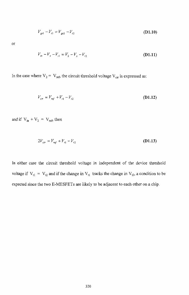
^^1-^ .1=^^2-^ .2 (Dl.lO)
or
Kr.-K-Vn=V,-K-V„ (DLll)
In the case where V2 = V f, the circuit threshold voltage Vg„. is expressed as:
^c,>=^.e/+^.1-^.2 (D1.12)
and if Vi„ + V2 = Vref, then
2K>r=Kef+K,-V,, (DL13)
In either case the cfrcuit threshold voltage in independent of the device threshold
voltage if V^ = Vt2 and if the change in V i tracks the change in Vt2, a condition to be
expected since the two E-MESFETs are likely to be adjacent to each other on a chip.
320

Appendix E
Gallium Arsenide MESFET Layout
Methodology
El.O Lambda Based Layout Rule
The lambda based design rule was made popular by Mead and Conway [107] for
silicon, and are based on single parameter, lambda (X), which characterises the linear
features as well as the resolution ofthe complete wafer implementation process. Table
El.O and Figure ELI illusfrate the lambda based rule set [74]. From Figure ELI it can
be seen that the rule set is defined in terms of feature size, separation and overlaps.
Although diffusion, metal 1, and metal 2 can cross each other without interaction , in
some processes metal 1 is not permitted to cross diffusion. There are two types of
unplant used to form the two different transistors. It is essential for gate metal (red) to
321

Table El.l Lambda based layout rule for GaAs MESFET
Layer
Diffusion
Depletion
implant n
CIF Code
GD
GI
Al A2 A3 A4
BI
B2 B3 B4
Rule Feature
width
spacing
ton^ E-MESFET widtii
D-MESFET gate overlap
width
spacing spacing to E-MESFET
Dimension -
Lambda (X)
5
5
5
5
2
7
5 2
Ohmic
contact
GH Cl contact width
Gate metal GP
Contact GC
Metal 1 GM
C2 C3
DI D2
D3
D4
D5
D6
El
E2
E3
Fl
F2
F3
F4
spacing cut overlap
gate metal extension
gate metal length
gate metal width
cut overlap
gate metal spacing spacing to ohmic contact
cut size
cut spacing
spacing to via
width
spacing
cut overlap
via overlap
5 2
2
3 3
2 5
3
4 x 4
4
4
4
5
2
2
Via GV GI via size 5 x 5
322

G2 via spacing 5
Metal 2 GN HI width 5
H2 spacing 5
H3 overlap of via 2
completely cross the implant (green) region, otherwise the ttansistor that has been
created will be shorted by a n' path between source and drain. To ensure that this
condition is satisfied, 2X of gate metal extension is necessary. This is known as
Schottky extension.
Orientation of GaAs MESFETs is an important consideration during layout. All
MESFETs need to be positioned horizontally owing to the anisotropic nature of GaAs,
which influences the threshold voltage of the device. There are several enhancements
that may be added to the GaAs process, primarily to provide active load, capacitors,
resistors and to increase routability ofthe circuit through a third metal layer.
The approach taken here has been to focus attention on the main features of a typical
design rule that a VLSI designer must become familiar with.
E2.0 Layer Encoding and Layer Connectivity
The layer coding used for GaAs MESFET layout is presented in Figure E1.2. The
coding has been complemented by monochrome encoding ofthe lines so that black and
323

Al , A2
Green
A3
D3 - •—
D5
Fted
Red over green
D2
-H'^3^*-J_
\iii\ :tii ^ ^ ^ y « i UH ^^M',iii\
^^^^•'//^^///^^///^/// ^9 ^S h^-\^
MititilUtiiii\VAiiiiiiiiiiitt
\tii:iiii \tiiiiiii •AUli'Ai
«««<««<««*«««««««««<
Ohmic metal over active
E3«
Figure El.l Lambda based rules for GaAs MESFET process.
white copies of cfrcuit representation using ring notation do no loose the layer
information. In GaAs MESFET layout, intersections on the same layer form
intercormections as in Figure EL3(a). Intersections on different layers do not form
324

connection or tt-ansistors as shown in Figure EL3(b). Different layers may also be
connected by a contact or a via as shown in Figure E1.3(c).
Layer
Diffusion/ implant
Gate-metal
n+
Ohmic contact
K4etal1
Meta)2
Contact
Vial
Overglass/ passivation
Color
Green
Red
Yellow
Brown
Blue
Dark blue
Black
Gray
White stipples
CIF
GD
GP
GI
GH
GM
GN
GC
GV
GG
MONOCHROME ENCODING
WMMMM, m^^mm^
» 1
• 1
,j..}..j..L.|..|..|..i..|..|..L.|..|..{.
\:::::::i
• ^
Figure El .2 GaAs MESFET layer encodmg [74].
Metal 1-metal 1 ^— Blue
1
Metal 2-metal 2
• I - Dark blue
1
Diffusion-diffusion - i « - Green
\
Metal 1 Blue
i Metal 2 Dark blue
Metal 2 Dark blue
i Diffusion
'Green
Ohmic contact
Metal 2 Dark blue
Diffusion Green
MetaM Blue
Metal 2
Dark blue
(a) Same layer cormection
(b) Different layers no cormection
(c) Different Layers cormection by contact
Figure E 1.3 Layer connectivity [74].
325

E3.0 ISD GaAs VLSI Design Sequence
The design cycle usually followed usmg ISD VLSI Phase I software is illusfrated m
Figure El.4. The Phase I suite consists ofthe following tools:
(i) PLAN a powerful mask level graphic full custom layout tool.
(ii) SEE a general purpose graphic display tool.
(iii) CHECK a fast comer based design mle checker.
(iv) GAASNET an accurate and efficient GaAs cfrcuit extractor, and
(v) ELEC a versatile electrical rules checker.
togetiier witii tiuee utility programs P2C, C2P, and POINTS.
Figure El .4 Phase I VLSI design cycle.
326

E3.1 PLAN
The tool PLAN is a menu driven, fixed grid, lambda based interactive graphic screen
editing tool for Manhattan geometry VLSI design. The mask level layout of the cfrcuit
is designed and edited using the PLAN. The syntax for general PLAN command is:
plan [ -[options] ] [<filename>]
The available options in PLAN are:
V version
u brief user summary
i tum off information message
t <name> set technology
o <name> set screen driver
r <number> set replay mode
Typical PLAN graphic display is shown in Figure El.5.
E3.2 SEE
The tool SEE is a multimode VLSI cfrcuit viewing aid designed to draw from a CIF
cfrcuit description a scaled representation of the cfrcuit masks on a variety of screen.
The syntax for the SEE command is:
327

see [ -[options] ] [<filename>]
The available options in SEE are:
choose default values
t <name> set technology
u brief user summary
0 hard copy device
print program identification
While in SEE there are a number of uiteractive keyboard commands available to enable
the user to move about the design easily.
PLAN; Licenced by Integrated Silicon Design
Pick Object Instance point 4*1 boundary is 0,0 240,120 Cell: adder4
bbox 0.0 10,10
Tech: cmds T-T-T -I—r Ti—r 1—I—I—r—T—r
m\^^
\'.^iZZZiZZ2 m
m i;|2!zzz
im
ITTT
ilM^ZZ"
2ZZZZ]
1} TTTTTTTTl aad«r.pn
///^^^/\ ^ZZZZZk f
@ ^ f f i | ^ i
DE
i l ^
i;H2
1
u DH
'ZZZ
'ZZL\
ZZ3
ED 7 7 7
ZZZ
in:]iiiiiiiiiiiiii[:iiiii];:sii§oiiiiii{ii:]i{ii:iiiiiiiiin
' • ' ' ' ' • ' • I ' ' ' ' • t _ J ' ' ' • t — L .
Ct»
^ TT One en 9wnnw Isw ws 2es se
3CXI gCGC: nCS ?Z>
icwn cCCi d C D Q
cba cba cba
' i 3 4 5<>7«<) iRef.I 8Ref.2 7Ref.3
(OhmPt SOtunNt SNtnm 4Ptran
VsCut oVdcut jIMcut hPlcut
qQuit eEdit sSave -Retun fFilin ttUn-Do aArea xWindo yMove kKill tTag vWire bbox THelT
Figure E1.5 PLAN graphic display.
328

E3.3 Check
The tool check is a fast comer based VLSI circuit verification tool designed to detect
geometrical design rule errors. The use of CHECK enables the designer to ensure that a
design is fiilly compatible with the design rules of a particular fabrication process. The
input required by CHECK is a CIF file describing the design. The output provided by
the program is a design rule error file or a screen listing containing the list of errors
found, a brief description of each, and a report ofthe location in lambda coordinates of
the error. The syntax for the CHECK command is:
check [ -[options] ] [<filename>]
The available options in CHECK are:
c lists the CIF file being parsed
f<name> flatten geometry to a file
I <number> sets lambda value
0 <name> sends check message to a file
r lists design rules
t <name> set technology type
s <tx ty> set tile width and height
w <lx ly UX uy> window a section of design to be checked
u brief user summary
V print program identification
329

E3.4 GAASNET
GAASNET is a VLSI circmt verification tool used to extract a net list description and
other relevant design mformation from the circmt description file expressed in CIF. The
syntax for the GAASNET command is:
gaasnet [ -[options] ] [<filename>]
The available options in GAASNET are:
c lists the CIF file being parsed
f <format> set output format to one of SPICE, PSPICE or HSPICE
R select Raytheon MESFET model. The default is the
Curtice MESFET model
z select low frequency MESFET model
The cfrcuit simulation is performed using HSPICE cfrcuit simulation suite consisting of
HSPICE, HSPLOT and the necessary Graphical Simulation Interface.
E3.5 ELEC
The tool ELEC is a VLSI cfrcuit verification tool designed to operate on the netiist
circuit description. ELEC is designed to give the user feedback on the electrical aspects
of a design so that informed decisions can be made about the correctness or otherwise.
330

ELEC uses as its mput the extracted cfrcuit description generated by GAASNET. The
syntax for the ELEC command is:
elec [-[options] ] [<filename>]
The available options in ELEC are:
i information listing
t <name> set technology
V print program identification
o <name> write to ELEC wanting file.
331

Appendix F
Adder Design and Performance of
Components of Power Series Evaluator
Fl.O Adder Design
The fimctional representation ofa fitil adder is shown in Figure Fl.l. The operation of
an adder is described by the tmth table shown in Table Fl.l where A and B are the
input bits to be added, C is the carry-in from the previous stage, S is the sum-out and
Cout is the carry-out.
A -
B -
Cany-in (C)-
FuU Adder
Sum(S)
Cany-out (C
Figure Fl.l Full adder functional block diagram.
The boolean expressions for the two outputs S and Com can be obtained using kamough
mapping technique shown in Figure F1.2.
332

Table Fl.l Truth table for a fiiU adder
Inputs
A
0
0
0
0
1
1
1
1
B
0
0
1
1
0
0
1
1
C
0
1
0
1
0
1
0
1
Outputs
S
0
1
1
0
1
0
0
1
^out
0
0
0
1
0
1
1
1
BA 00 01 11 10
C 0
1
0
1
1
0
0
1
1
0
BA 00 01 11 10
C 0
1
0
0
0
1
1
1
0
1
S (Sum) Cout (Carry-out)
Figure Fl .2 Kamough map for S (Sum) and Cout (Carry-out)
Sum and Carry-out are expressed as follows:
Sum = A'B'C + A'BC' + AB'C' + ABC (Fl.O)
Carry-out = A'BC + AB'C+ ABC + ABC (Fl.l)
Using De'Morgans theorem, expressions FLO and Fl.l can be expressed as:
Sum = {A + B + C) + {A + B' + C) + (A' + B + C) + {A' + B'+C) (F1.2)
333

Carry-out = {A'-hB')-i-(A'-{-C') + {B' + C') (ri.3)
F2.0 VLSI Mask Layout and Simulation ofthe components
of Power Series Evaluator Cell
The VLSI layout and HSPICE smiulation results for the adder, two-to-one multiplexer
and tiie register are shown in Figures F 1.3 - F 1.8. The circuits were unplemented usmg
0.8 micron E-D GaAs MESFET technology usmg ISD VLSI design suite.
SKCout
Figure F1.3 Mask layout of an adder.
-6i|tld
Figure F1.4 Mask layout of a two-to-one multiplexer.
334

Figure F1.5 Mask layout of an one-bfr register.
flOD.TRO VINl
0 I 50 0. OM r /• r r • / i / • • • • : 1 L N f. z- . J.. . I J.. i . . .1. .w4»-( • J . ' . • I . 1 .1 / • . 1 . . . . 1 . . • 1 . . . t . V . I . ••• 1
: J flDD.TRO ' • • • : V INS
i . - . J . . ^ ^ - ^
— flOD.TRC
0 .
STL go.oHr I ••(•••t-1 [ -b- i^- f [••• - . flOI U - ' 1 ^ ~ - 1 •-- t - ^ - V ^ ^ L _ ; ^ pQ^j-p TTN L . . j . . . i . . . i . . . i . . . . i . . . j . . . . . . . L . . . i . . . J . . . i . . . i . . . i . . . . i . . . J . .J i ^
5 .ON I O . O N 15 .ON 0 . TIME CLINO 16 .ON
Figure F1.6 HSPICE sunulation results for an adder. VINl - VINS represent inputs A, B, C and outputs Sum and Carry out respectively.
335

V L 0 I L N
5 00 . OM
I- . J . . . I . . . I . . .1 1 ! I I . . .1 I. . . I . . . I I I I 2,
V L 0 I 500.OM L N 1 . . . 1 . . .u . . . 1 .
V L 0 I L N
V L 0 I L N
5 0 0 .OM
500.OH
I . . . 1 ,
0 .
V L p i 5 0 0.OM
•- ' 0 .
5 . 0 M
0 .
J . . . I . . . i r m r TtTTrYS
llfTL AOI TTN
IZL . J . . . I . . . 1 . . .1 . . . . 1 . . . J . . . I . . .L . . .1 . . . J . . . , .
5.ON 10.ON 0- TIME CLIN}
MUX.TRO - V I N l
~ 1 1 . . . . . . . . i . . . 1 • . . . j . . . . . . . 1 — 1 . M
1 ^ . .3
MUX .TRO VIN2
J MUX.TRO : VIN3 ^ t^
MUX .TRO VIN**
&-
u MUX.TRO VINS
— MUX.TRO POWER
15.ON IS . ON
Figure F 1.7 HSPICE simulation resufrs for a two-to-one multiplexer. VINl and VIN2 represent the inputs J and T, VIN3 and VIN4 represent the true and complementary mux control and VINS represents the mux output.
V L Q I 500.OM — L N
0.
V L 0 1 5 0 0.OM
L ' 0.
. .1. .L .1. .L .1. .L .1 .
jz F F D . T R O = ^VINl
. I . I . I . I _3 "
C-i. .1. .1. .1. .1. .1. .1. . 1. . L . 1 . L I . L . 1 .
^ F F D . T R O Z VIN2 T 5:
Q J 50 0. OH f
l. N
"
: , 1 uJ 1 1 1 1 . . 1 . . 1 1 J 1 1 1 f
z
' ' 1 1 1 1 • A
F F D . T R O VIN3
y *• 500 O M ^ ; : • • • • • / • • • ? : . . . . \ . . . . : -_ F F D . T R I
•L N ,, Z_l . \»;vJ • I • ' ' • I—•—i-t' • I I • < • I I • \ I 1 1 1 1 L J I "
V L jj J 5 0 0.0M = = ^ " . — : : — \ "
L N . : _ i . . 1 . . 1 . . 1 . . 1 . . i ! . 1 . . 1 . .1 . .L .k .L .> L.
.: - FFD.TRO
i . i . L i . i . i . u ^
»TL flOI 1 0 . O M
TTN :::t:::4jLim::4-:u
: FFD.TRO POWER
I. . 1 . .1 . . 1 . . 1 . . 1 . . t . .1 . .1. .[. .1 . .L . 1 . .L .L .L . 1 . 1 . 1 . . t . 1 . 1 . [ . I . t . I . I . r_3
• 2.SON 5.ON 7.50N I 0 . ON 12.50N 0. TIME CLIN) 15.ON
Figure F1.8 HSPICE simulation results for an one-bfr register. VINl and VIN2 represent the flip flop true and complementary inputs respectively, VIN3 the clock (phi), VIN4 and VINS represent the flip flop true and complementary outputs respectively.
336

Appendix G
Inverse Time-Current Characteristics
An equation for inverse time-current characteristics can be derived from the following
basic differential equation for input time delay as it applies to a induction relay [110]:
x^(I"-l) = K,^ (Gl.O) at
where x^ is the spring torque
/ is the current in multiple of tap setting
n is an index characterising the algebraic function
K^ is the damping factor due to drag magnet
9 is the angular displacement and
dQ/dt is the angular velocity.
The small moment of inertia of the disc is neglected and the spring torque is
represented by a constant because the effect of its gradient is compensated by an
increase in torque caused by the shape ofthe disc. Integrating equation 1.0 given:
e^j^ToT^(r-i)^^ (Gi.i)
^d
337

Dividing both sides ofthe equation Gl.l by 0 gives the dynantic equation:
jToX,(r 1)^^ ^ l.'^'^-^dt = 1 (G1.2) K,.Q " t{I)
Thus the inverse-time characteristic is given as:
T = t{I)= ' • '" (G1.3)
where T is the theoretical operating time ofthe relay
K is the design constant K , and
t^ is the time multiple settuig.
338

Appendix H
Four-Bit Encoder
Hl.O Design Procedure
The encoder translates the outputs of the comparators mto a final binary outputs. The
inputs to the encoder is fed from the comparators, as shown. The following steps are
used to develop the truth table for the encoder [117].
(i) Start with 2 "" comparators and label them in the ascending order as
shown in Figure 8.2. The non-inverting input of all the comparators
are cormected to the sampled analog input voltage. The inverting input
ofthe comparator YQ (MSB comparator) is set to Vrgf/2.
(ii) The output of this comparator, (YQ), is used to control the switches,
which have their outputs cormected to the inverting input ofthe other
comparators. The inputs ofthe switches are connected to the
appropriate portions ofthe reference voltages. The output ofthe
comparators are presented in Figure Hl.l for different values of input
voltage, Vin.
339

Input Voltage
Vi„<V,,/16
Vref/16<Vi„<2V,/16
2V,ef/16<Vi„<3V,,f/16
3V,e/16<Vi„<4V,e/16
4V,e/16<Vin<5V,,f/16
5V,ef/16<Vi„<6V,ef/16
6V,,/16<Vi„<7V,,/16
7V,ef/16<Vi„<8V,,/16
8V,f/16<Vi„<9V,ef/16
9V,ef/16<Vi„<10V,,f/16
10Vref/16<Vin<llV,e/16
llV,e/16<Vi„<12V,e/16
12V,e/16<Vi„<13V,e/16
13V,e/16<Vi„<14V,e/16
14V,ef/16<Vi„<15V,e/16
Vi„>15V,/16
X
15
0
0
0
0
0
0
0
0
0
0
0
0
0
0
0
1
X
14
0
0
0
0
0
0
0
0
0
0
0
0
0
0
1
1
X
13
0
0
0
0
0
0
0
0
0
0
0
0
0
1
1
1
X
12
0
0
0
0
0
0
0
0
0
0
0
0
1
1
1
1
X
11
0
0
0
0
0
0
0
0
0
0
0
X
10
0
0
0
0
0
0
0
0
0
0
X
9
0
0
0
0
0
0
0
0
0
X
8
0
0
0
0
0
0
0
0
X
7
0
0
0
0
0
0
0
X
6
0
0
0
0
0
0
X
5
0
0
0
0
0
X
4
0
0
0
0
X
3
0
0
0
X
2
0
0
X
1
0
Figure Hl.l Outputs of the comparators for a four-bit flash ADC.
(iii) The output ofthe comparator is encoded into binary outputs using the
tmth table of Figure Hl.l. The values of YjS are computed using the
following expressions:
Y, = MSB=X^ (Hl.O)
Y\ - ^M-\ • ^M + ^ M + 1 • ^M (Hl.l)
340

In general, for I = 1,2, 2 n-l
Yi - ^M-i • ^M + ^M+i • ^M (H1.2)
n-l where MSB comparator output in a classical flash ADC is XM and M = 2 ' . Now the
YjS can be encoded to obtam the proper binary digits D, C, B, and A. The encoded
outputs are presented in Figure HI .2.
Yo
0
0
0
0
0
0
0
0
Y,
0
0
0
0
0
0
0
1
0
Y2
0
0
0
0
0
0
1
1
0
0
1
1
1
1
1
1
Y3
0
0
0
0
0
1
1
1
0
0
0
Y4
0
0
0
0
1
1
1
1
0
0
0
0
1
1
1
1
Y5
0
0
0
0
0
0
0
0
1
1
1
Y6
0
0
0
0
0
0
0
0
1
1
Y7
0
0
0
0
0
0
0
0
1
D
0
0
0
0
0
0
0
0
c
0
0
0
0
1
1
1
1
0
0
0
0
1
1
1
1
B
0
0
1
1
0
0
1
1
0
0
1
1
0
0
1
1
A
0
1
0
1
0
1
0
1
0
1
0
1
0
1
0
1
Figure HI .2 Relationship between comparator and encoder outputs for the proposed four-bit flash ADC.
341

The Kamough map method is an effective way to simplify switching fimctions which
have a small number of variables. When the number of input variables is large, as is in
this case, or if several fimctions must be sunplified, kamough map method becomes
very tedious and altemate approach to simplification of boolean fimctions is needed.
The Quine-McCluskey method [112] is one such approach that provides a systematic
simplification procedure for boolean functions with large number of input variables.
Hl.l The Quine-McClusky IMethod
The Quine-McClusky procedure reduces the minterm expansion (standard sum-of-
products form) of a function to obtain a minimum sum of products. The procedure
consists of two main steps:
(i) Eliminate as many literals as possible from each term by
systematically applying the theorem X.Y+X.Y = X. The
resulting terms are called prime implicants.
(ii) Use the prime implicant chart to select a minimum set of prime
implicants which, when ORed together, are equal to the
function being sunplified and which contain a minimum number
of literals.
342

The objective of obtaining the set of prime implicants is achieved through the foUowing
steps:
(i) Express the fimction in expanded sum-of-products form or as a
sumofminterms.
(ii) Represent each minterm by its minterm number in binary form.
Note that variables must be ordered in accordance with
weighting.
(iii) Make a table of terms, ordering them according to index (index
is equal to the number of one's in the bmary representation, eg.
0100, 0001, are of index 1, 1001, 0110, are of mdex 2, etc.).
(iv) By making groups, where ever possible across boundaries
between terms which differ by 1 in index, form a second table of
grouped terms ordered again by index and replacing grouped
variables by a dash (-), (ie. where a zero and a 1 have been
grouped). Terms will group when they differ in only one literal,
eg. 001 will group with 101 to form -01,100 groups with 110
to give 1-0, etc.
(v) Tick all terms which have to be grouped. Unticked terms must
appear m the final prime implicant (PI) set.
343

(vi) Repeat the grouping exercise across the index boundaries with
the constraint that dashes must also line up for grouping to be
possible.
(vii) Continue the grouping procedure, forming subsequent tables
until no further grouping is possible.
(viii) The terms in the fmal table together with all unticked terms in
all previous tables constitute the PI set.
Having obtained the PI set the second objective of the procedure, namely choosing the
optimum set of Pi's is then achieved. One way of so doing is to use a PI chart. The
Quine-McClusky procedure is illustrated by way of an example below.
HI.1.1 Example
Use the Quine-McClusky procedure to find the simplest realisation of the function T
where:
T^l^l^lC.Z + X.Y (H1.3)
The process is as follows:
(i) Express T in expanded SOP and binary forms:
344

T^XH^'XJ.Z^'X.Y.Z^X.YI^X.Y.Z (H1.4)
= 000 -I- 001 + oil + 110 + 111
= Sm(0,1,3,6,7)
(u) Set out tables (Table HI. 1 and HI .2) accordmg to mdex and carry out
the grouping process.
Table Hl.l Quine-McClusky grouping process - first iteration
Index
Zero
One
Two
Three
m
0
1
3
6
7
Terms
V V V V V
000
001
oil
no 111
Table H1.2 Quine-McClusky grouping process - second iteration
Index
Zero
One
Two
m
0,1
1,3
3,7
6,7
Terms
A
B
C
D
00-
0-1
-11
11-
No grouping is possible in table hi.2 because dashes do not line up across any
boundary. Therefore identify all unticked terms A, B, C, and D to form PI set. The PI
set for this example is thus:
345

T=A+B+C+D (H1.5)
(iii) The PI chart is set out as shown in Figure HI .3.
PJ. Set
<4'j First stage
T
^ A .
B-
C -
D-
- ;
•illnter
P s — •
— i
•ms Dresenf In 'T
1
•
; —
•
3
\
6 7
P.I. Set
B.
Essential P.U
Stage
c
(b) SecondN^ /TN
Minterms oresant Irt 'V
PV 1V ,3 6V 7V
^ ) ^•
Jr-^
# - ^ r
Figure HI.3 PI chart.
(iv) Circled Pis are the essential Pis since they cover minterms which are
not covered by any other PI. The essential Pis must be present in any
solution for T.
(v) Choose Pis as economically as possible to cover the remaining
minterms. (In this case either PI B or C will do equally well since they
are equal size groups).
(vi) Final solution as a set of Pis and algebraic form are:
T=A + D+B or C (H1.6)
= 00- + 11- + 0-1
= X.Y+X.Y+X.Z (H1.7)
346

The expressions for tiie four outputs (D, C, B, and A) were simphfied using the Quine-
McClusky procedure and are expressed in terms ofthe comparator outputs as foUows:
D = Y, (H1.8)
C=Y, (H1.9)
B = (Y,+Y,).{Y,+Y,).{Y,+Y,) (Hl.lO)
A = {Y, + YMYs + Y,).{Y,+YMY2 + Y,).(Y,+Y,).
{Y,+YMY:+Y,) (Hl.U)
where YQ, 77 are the ou^uts ofthe eight comparators.
The OR/NOR based logical representation of the four-bit encoder is shown in Figure
8.4. Due to degradation of performance, the encoder circuit is limited to parallel
branches in the input, ie., OR/NOR stmcture ortiy. GaAs Merged logic design
techruque has been used to design the OR/NOR gates for the encoder.
347

Appendix I
Eight-bit Comparator
II.0 Design Procedure
This section describes the design of a cascadable comparator cell using Merged GaAs
MESFET logic. An eight-bit comparator was designed using cellular structure of cells.
The general arrangement and the truth table for a binary one-bit comparator bit-slice is
shown in Figure 11.1(a) and (b), where A; and Bj are the two multi-bit numbers to be
compared, Cj+i is tiie input from the output ofthe previous stage, and Cj is the output of
the current stage. The behaviour ofthe cell is described £is follows:
Cj = 1 for Aj > Bj, and
Ci = 0 for Aj = Bj and/or Aj < Bj.
348

Bi Ai
M^ M/"
Ci.l ^ Comp^arator ^ ,
Figure 11.1(a) Bit-slice comparator cell.
Cj+l
0
0
0
0
1
1
1
1
Aj
0
0
1
1
0
0
1
1
Bi
0
1
0
1
0
1
0
1
Ci
1
1
0
1
0
0
0
0
Figure 11.1(b) Comparator cell truth table.
The output, Cj, in terms of the inputs are plotted on the kamough map as shown in
Figure 11,2.
AiB
00 01 11 10
C, i+l
0
1
1
0
1
0
1
0
0
0
Figure 11.2 Kamough for Ci.
349

The minimised logical expression for Ci can be expressed as:
q = q,,+4.5, ai.o)
C,=(C,,, + 4.j5,)
q = q^,.(A,+B,)
Q = Q , + ( 4 . + 5,) (ii.i)
Expression for C; described by equation 11.1 can be implemented using NOR gates.
The logical implementation ofa single bit comparator cell is shown in Figure 11.3.
SI .
Bi_
Ci+l- I> Ci
Figure 11.3 Logical representation of a comparator cell.
350

Appendix J
Design and Performance ofa Four-Bit Time-
Out Timer Using J-K Flip Flops
Jl.O Timer Design Procedure
The procedure used to design a four-bit time out timer is summarised as follows:
(i) Derive a state table from state graph or problem statement.
(ii) Plot the next state maps from the state table.
(iii) Plot the J-K input map for each flip flop.
(iv) Derive the J-K input expressions for each flip flop.
(v) Realise the circuit using J-K flip flops and additional logic.
Table J 1.1 (a) describes the next state output for a J-K flip flop as a function of the
synchronous inputs and present state output. Using this, the required input conditions
for J and K when Q and Qn+i are given are derived. Thus if a change from Q = 0 to Qn+i
= 1 is required, either the flip flop can be set to 1 by usmg J = 1 and K = 0 or the state
351

can be changed by using J = K = 1. In other words J must be 1, but K is a don't care.
The J K mput requfrements are summarised m Table Jl .1 (b).
Table Jl.l J K flip flop next state outputs
J
0 0 0 0 1 1 1 1
K
0 0 1 1 0 0 1 1
Q„
0 1 0 1 0 1 0 1
Qn+1
0 1 0 0 1 1 1 0
Q
0 0 1 1
Qn+1
0 1 0 1
J
0 1 X X
K
X X 1 0
(b)
(a)
The state table for a four-bit time out timer is shown in Table J 1.2 with columns added
for the J and K flip flop inputs. The input columns are completed using the results in
Table Jl. 1(b).
352

Table J1.2 State table and input controls for a four-bit timer
D C B A
0
0
0
0
0
0
0
0
1
1
1
1
0
0
0
0
1
1
1
1
0
0
0
0
1
1
0
0
1
1
0
0
1
1
0
0
1
1
0
0
1
0
1
0
1
0
1
0
1
0
1
0
1
0
1
0
D^ C^ B^ A^
0
0
0
0
0
0
0
0
1
1
1
1
0
0
0
0
1
1
1
1
0
0
0
0
1
1
0
0
1
1
0
0
1
1
0
0
1
1
0
0
1
0
1
0
1
0
1
0
1
0
1
0
1
0
1
0
1
JD
X
X
X
X
X
X
X
X
0
0
0
0
0
0
0
1
KD
0
0
0
0
0
0
0
1
X
X
X
X
X
X
X
X
Jc
X
X
X
X
0
0
0
1
X
X
X
X
0
0
0
1
Kc
0
0
0
1
X
X
X
X
0
0
0
1
X
X
X
X
JB
X
X
0
1
X
X
0
1
X
X
0
1
X
X
0
1
KB
0
1
X
X
0
1
X
X
0
1
X
X
0
1
X
X
JA
X
1
X
1
X
1
X
1
X
1
X
1
X
1
X
1
KA
1
X
1
X
1
X
1
X
1
X
1
X
1
X
1
X
•»+.^+T^+ • + DCBA and D C B A are the outputs of the timer immediately before and after the clock transition.
The J K maps of Figure Jl.l are obtained directly from Table J 1.2. The J and K input
expressions for each flip flop are derived using kamough maps of Figure Jl.l.
BA 00
DC
00
01
11
10
01 11 10
1
0
X
X
0
0
X
X
0
0
X
X
0
0
X
X
BA 00 01
DC
00
01
11
10
11 10
X
X
0
1
X
X
0
0
X
X
0
0
X
X
0
0
J^^C.B.A Kj,=C.B.A
353

BA
DC
00
01
11
10
00 01 11 10
1
X
X
1
X
X
X
0
X
X
X
0
X
X
X
0
BA 00
DC
00
01
11
10
Jc = B.A
01 11
BA 00
DC
00
01 11
10
J,=A
01 11
10
1
1
1
1
0
0
0
0
X
X
X
X
X
X
X
X
10
1
1
1
1
X
X
X
X
X
X
X
X
1
1
1
1
J, = l
BA
DC
00
01
11
10
00 01 11
X
1
1
X
X
0
0
X
X
0
0
X
Kc = 'B.1
BA 00 01 11
DC
00
01
11
10
X
X
X
X
X
X
X
X
0
0
0
0
K, = A
BA 00 01 11
DC
00
01
11
10
X
X
X
X
K
1
1
1
1
. = 1
1
1
1
1
10
X
0
0
X
10
1
1
1
1
10
X
X
X
X
Figure Jl.l Flip flop input maps.
The expressions for the inputs can be transformed into GaAs technology implementable
form by using De Morgans theorems. The transformed expressions for the J K flip flop
inputs are expressed as:
354

JD=KO=(C + B-\-A) (Jl.O)
Jc = Kc={B + A) (Jl.l)
JB=K,=A (J1.2)
J, = K,=l (J1.3)
The four-bit time out timer is implemented using J K flip flops and NOR based logic
for the input controls. The clock input of the flip flops are cormected together to give a
synchronous operation. The logical cfrcuit of an one-bit time out timer is shown in
Figure 9.13.
Parallel load is facilitated by enabling a synchronous load signal which causes the
parallel input data to be fransferred to the output on the next clock pulse. The tuner also
has asynchronous preset and clear functions.
J2.0 Timer Performance
The performance ofa one, two and three-bit time-out timer is shown in Figures J1.2
J1.4.
355

l .OVi-.
o.ov l .OVf
l...LLi....L.UL.i..J :LJ...iM .i...li >v(phl)
0.0V+ m o?(c l ) "vCpr)
Ji ~|-
l.OVf.
0 . 0 V 4 - ^ »vdd
l .OVf
0.0V+-
1 . OV f H 1
oVfa 1. OV t 1 1
o.ovhnL^....i u = 0ns 20ns 40ns
••vtq, . .
H—r~ii r ~ h
=u ^ n — I -
60ns 100ns
TiBB
Figure J1.2 Performance of an one-bit tuner.
1.0V+;
O.OV I._LLi...l.lJ...L_ULl..L.U..Ji l.OVi—
o v ( p h l l )
0.0V +
l.OVH OV (prSJ
0.0V+-
—h
— h
--+ i.ovt-aV(prl)
l . O V f — ^ J . J ^ ^.
O.OV.) 0ns
•>v (b) 20ns 40ns 80ns
Time
u lOOns
Figure J1.3 Performance ofa two-bit timer.
1.0V+-
i n NLLLi..l.U...lJ 0.0V+— oVIphll)
l .OVH
O.OV.I
1 . 0 V 4 -
u ^-^\l^\J^v^\.^^J »v (a )
0.OV+-
l.OVH
u .vto)
o.ov^— Ons
• V tc) 20ns
n u
40ns sons
Time
eons 100ns
Figure J1.4 Performance of a three-bit timer.
356


